
Recent development and understanding of polymer–nanocrystal hybrid solar cells
Zhaolai
Chen
ab,
Xiaohang
Du
a,
Qingsen
Zeng
a and
Bai
Yang
 *a
*a
aState Key Laboratory of Supramolecular Structure and Materials, College of Chemistry, Jilin University, Changchun 130012, P. R. China. E-mail: byangchem@jlu.edu.cn
bDepartment of Mechanical and Materials Engineering, University of Nebraska-Lincoln, Lincoln, Nebraska 68588, USA
First published on 8th February 2017
Abstract
Solar cells are being rapidly developed nowadays due to the limited resources of fossil fuels and the worldwide growing energy demand. Polymer–nanocrystal solar cells (HSCs) are promising candidates thanks to the lightweight and mechanically flexible properties of polymers and the adjustable absorption, high carrier mobility, and superior structural stability properties of nanocrystals. However, compared with polymer–fullerene/organic molecule solar cells (PSCs), the development of HSCs is relatively sluggish, which is due to the complex characteristics of the polymer–nanocrystal system and the incomplete understanding of the operation mechanism. This review gives a brief introduction to device structure and operation mechanism of bulk heterojunction HSCs, and the differences between HSCs and PSCs will be emphasized. Recent work that has been done to improve the device performance or clarify the operation mechanism is summarized and discussed in detail. Both organic-solution-processed and aqueous-solution-processed HSCs will be discussed. Finally, the challenges and perspectives of HSCs will be presented.
 Zhaolai Chen | Zhaolai Chen is a postdoctoral researcher in the Department of Mechanical and Materials Engineering, University of Nebraska, and the State Key Lab of Supramolecular Structure and Materials, Jilin University. He received his PhD in polymer physics and chemistry in 2016 under the supervision of Prof. Bai Yang at Jilin University. His research is centered on aqueous-processed polymer/nanocrystals hybrid solar cells and single-crystal hybrid perovskite solar cells. |
 Xiaohang Du | Xiaohang Du graduated from Jilin University in 2013. She is now a PhD student at the State Key Lab of Supramolecular Structure and Materials, majoring in polymer chemistry and physics. Under the supervision of Prof. Bai Yang, she is working on the improvement of polymer/nanocrystals hybrid solar cells. |
 Qingsen Zeng | Qingsen Zeng is a PhD student at the State Key Lab of Supramolecular Structure and Materials, majoring in polymer chemistry and physics. Under the supervision of Prof. Bai Yang, he is working on the working mechanism and improvement of aqueous-processed polymer/nanocrystals hybrid solar cells. |
 Bai Yang | Bai Yang is currently a professor of chemistry at the State Key Lab of Supramolecular Structure and Materials in the College of Chemistry, Jilin University. He received his PhD in polymer physics and chemistry in 1991 under the supervision of Prof. Jiacong Shen at Jilin University. His current research interests are focused on polymeric carbon nanodots, polymeric nano-hybridization and photoelectric materials and devices via aqueous approaches, high-performance polymeric hybrid optical materials and ordered fabrication of polymeric microstructures with multi-scale and photonic responsive materials. |
1. Introduction
The limited resources of fossil fuels and the world-wide growing energy demand have caused the need to develop inexpensive renewable energy sources, which has stimulated scientific research for efficient, low-cost photovoltaic devices. PSCs have become promising candidates for offering low-cost solar energy conversion,1–4 since they can be fabricated by solution-based processing, such as spin-coating, printing, dip-coating, painting and roll-to-roll processing.5–8 They also show the advantages of being lightweight and mechanically flexible. In the past decade, great progress has been achieved in polymer–fullerene systems with power conversion efficiency (PCE) approaching 11%.9 However, the disadvantage of PSCs is that fullerenes contribute negligibly to the photocurrent due to their weak absorption property.10 In this regard, inorganic nanocrystals and organic small molecules with adjustable absorption property are proposed to replace fullerene.11–19 Here, we are concerned mainly with polymer–nanocrystal HSCs.20–25 Potential advantages of inorganic nanocrystals also include high carrier mobility, superior structural stability and facile exciton dissociation.26–30 In the past decade, the PCE of HSCs has been improved progressively by changing the size and shape of the nanocrystals, as well as by ligand exchange, thermal annealing, solvent-vapor annealing and device structure optimization.31–40 Recently, HSCs from water-soluble polymers and nanocrystals have been investigated by several groups as they can avoid the use of toxic solvents, such as chlorobenzene and chloroform.41–50 Up to now, the PCE of aqueous-solution-processed HSCs is comparable to that of counterparts based on organic solvent.51,52Compared with PSCs, the development of HSCs is relatively sluggish. This is due to the complex characteristics of the polymer–nanocrystal system and the incomplete understanding of the operation mechanism. Compared to fullerene, the existence of superficial defects and ligands greatly impacts the carrier transport and recombination,53–55 which complicates the optimization of the HSCs. The large difference of polarity between polymer and nanocrystals causes difficulty in morphology control and incomplete charge transfer,56–59 which is quite different from the polymer–fullerene system. Besides, there is still controversy about the essence of junctions in HSCs,60–63 which imposes extra difficulty in determining the optimization strategy.
Before 2013, it was challenging for HSCs to obtain PCE over 4%, which led to much fewer groups working on HSCs. However, there have now been a lot of reports demonstrating PCE around 5–6%.52,63–66 Meantime, new understanding of HSCs concerning charge transfer, transport and operation mechanism has been provided.67–71 Motivated by these recent developments, we believe that it is required to reconsider the limitations and optimization strategies of HSCs, aiming for further improvement of device performance. This article starts with a brief introduction to device structure and operation mechanism of bulk heterojunction (BHJ) HSCs. The differences between HSCs and PSCs will be emphasized. This is followed by recent work that has been done to improve device performance or clarifying the operation mechanism. Both organic-solution-processed and aqueous-solution-processed HSCs will be discussed. Finally, the challenges and perspectives of HSCs will be presented.
2. Device structure and operation principle of HSCs
The device structure of HSCs is very similar to that of PSCs: a photoactive layer consisting of polymer and nanocrystals is sandwiched between two electrodes with different work functions (Fig. 1a). Normal structure is widely used in HSCs where transparent indium tin oxide (ITO) serves as the anode and low work function metal serves as the cathode. In HSCs, the polymer and nanocrystals both contribute to photo-absorption. Polymer serves as electron donor and hole acceptor, nanocrystals serve as hole donor and electron acceptor. In comparison with PSCs, the polymer content is much lower in HSCs, which is required to control morphology and obtain high efficiency.56,62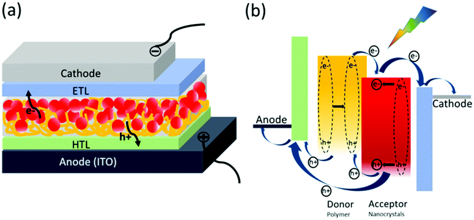 | ||
| Fig. 1 (a) Device structure of polymer–nanocrystal HSCs with formal structure. (b) The fundamental process in polymer–nanocrystal HSCs. | ||
In general, the fundamental process in polymer–nanocrystal HSCs involves five parts which are shown in Fig. 1b:
(1) When the active layer is illuminated, excitons are generated in both polymer and nanocrystals. The dielectric constant of nanocrystals is usually much higher than that of the polymer.11 Therefore, nanocrystals show more facile exciton dissociation ability and even exciton self-dissociation phenomenon.67
(2) Excitons diffuse to the polymer/nanocrystals interface. It is worth noting that excitons generated in the polymer should arrive at the interface within the exciton diffusion length; otherwise, adverse recombination will occur.1
(3) Excitons dissociate or charge transfer into free carriers. Energy offset between the lowest unoccupied molecular orbital (LUMO) level of the polymer and the conduction band (CB) of the nanocrystals is required for efficient electron transfer from polymer to nanocrystals. Likewise, energy offset between the highest occupied molecular orbital (HOMO) level of the polymer and the valence band (VB) of the nanocrystals is required for efficient hole transfer from nanocrystals to polymer. Unlike nearly complete charge transfer in PSCs, the weak interaction between polymer and nanocrystals leads to incomplete charge transfer between polymer and nanocrystals.56 In addition to electron transfer, the polymer funneling energy to nanocrystals via energy transfer has also been demonstrated in HSCs.68
(4) The free carriers are transported to the electrodes through bicontinuous pathways. In PSCs, polymer and fullerene participate in hole and electron transport, respectively. For HSCs, the facile exciton dissociation of nanocrystals and partial hole transfer mean the holes are transported by both polymer and nanocrystals. In contrast, only nanocrystals participate in electron transport.66
(5) When the free carriers reach the corresponding electrodes, charge extraction will occur. The interlayer is usually used to selectively extract carriers.
3. Recent understanding of HSCs
In spite of many advantages of nanocrystals over fullerenes, the PCE of HSCs is far lower than that of PSCs. Therefore, more efforts have been devoted to investigate the charge transfer and transport mechanism to discover the factors that limit the PCE of HSCs.3.1 Electron transfer
In the early work of HSCs, fluorescence quenching measurement was usually used to confirm the electron transfer.72 But this method was occasionally ambiguous when energy transfer could not be excluded. Recently, ultrafast transient spectroscopy was adopted to investigate the electron transfer between polymer and nanocrystals. In this case, electron transfer and energy transfer could be distinguished. Additionally, the electron transfer yield and its limitation factors could be estimated.Couderc et al. used ultrafast transient absorption spectroscopy to study charge transfer dynamics in hybrid films composed of poly[2,6-(4,4-bis(2-ethylhexyl)-4H-cyclopenta[2,1-b;3,4-b′]dithiophene)-alt-4,7-(2,1,3-benzothiadiazole)] (PCPDTBT) and CdSe nanocrystals capped with tert-butylthiol.58 Since the absorption onsets of CdSe nanocrystals and PCPDTBT are 600 nm and 850 nm, PCPDTBT could be selectively excited by light of 800 nm (Fig. 2a and b). However, a spectral signature for electrons of CdSe nanocrystals emerged (Fig. 2c), which indicated electron transfer from PCPDTBT to CdSe nanocrystals. Through quantitative analysis of the bleaching signal of CdSe nanocrystals at different times, the electron transfer was found to occur on an ultrafast time scale (∼65 fs) with a yield of about 82%. Nevertheless, diffusive models showed that most transferred electrons were spatially located close to polarons of PCPDTBT, which led to rapid recombination and low charge separation efficiency of less than 30%. Therefore, the authors concluded that a limitation of the hybrid system was rapid geminate recombination due to the small separation of the initial charge pair. In this system, the CB of CdSe nanocrystals was close to the LUMO level of PCPDTBT, which may also contribute to the inefficient charge separation. Guo et al. investigated the electron transfer between poly[2,6-(N-(1-octylnonyl)dithieno[3,2-b:20,30-d]pyrrole)-alt-4,7-(2,1,3-benzothiadiazole)] (PDBT) and PbS nanocrystals by ultrafast transient transmission spectroscopy.59 The energy offset between the LUMO level of PDBT and the CB of PbS nanocrystals (0.7 eV) was much larger than that of PCPDTBT–CdSe (0.2 eV). As shown in Fig. 3, the bleaching signal of PDBT showed a much faster decay (within 5 ps) in hybrid films than in the neat PDBT film. This indicated the occurrence of ultrafast electron transfer from PDBT to PbS nanocrystals. The estimated electron transfer yield of PDBT/PbS with ratios of 1/15, 1/10, and 1/5 was 79.8%, 69.2%, and 50%, respectively.
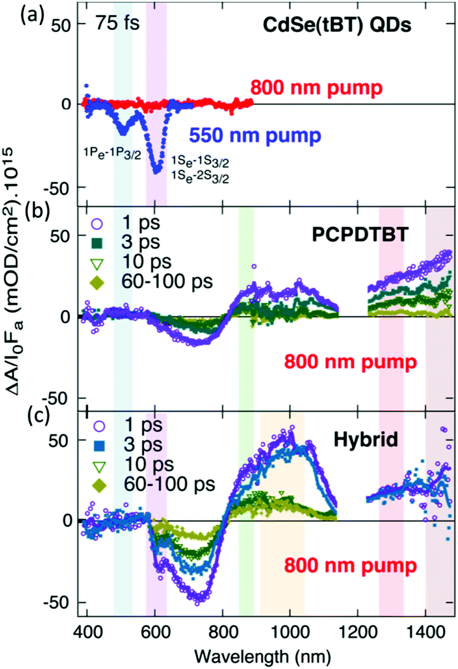 | ||
Fig. 2 Transient absorption spectra of (a) neat CdSe(tBT) film, (b) neat PCPDTBT film (15–20 nm), and (c) hybrid PCPDTBT![[thin space (1/6-em)]](https://www.rsc.org/images/entities/char_2009.gif) :CdSe(tBT) film (1:8 w/w, 45–55 nm) at different time delays between the pump and the probe pulses. I0 is the incident pump photon density (I0 ∼ 7.3 × 1014 cm−2 for the 800 nm pump; 5 × 1014 cm−2 for the 550 nm pump), while Fa is the fraction of 800 nm photons absorbed by the films (Fa ∼ 0.14 for both the polymer and the QD films, Fa ∼ 0.09 for the hybrid). Reproduced with permission from ref. 58. Copyright 2013, American Chemical Society. :CdSe(tBT) film (1:8 w/w, 45–55 nm) at different time delays between the pump and the probe pulses. I0 is the incident pump photon density (I0 ∼ 7.3 × 1014 cm−2 for the 800 nm pump; 5 × 1014 cm−2 for the 550 nm pump), while Fa is the fraction of 800 nm photons absorbed by the films (Fa ∼ 0.14 for both the polymer and the QD films, Fa ∼ 0.09 for the hybrid). Reproduced with permission from ref. 58. Copyright 2013, American Chemical Society. | ||
 | ||
| Fig. 3 Comparison of the normalized ΔT/T dynamics in neat PDBT film and PDBT/PbS quantum dots (QDs) hybrid film (nominal weight ratio 1/15) with a probe wavelength of 750 nm under a pump fluence of ≈50 μJ cm−2. The inset shows the band alignment between the PDBT and PbS QDs in the hybrid film. Reproduced with permission from ref. 59. Copyright 2016, Wiley-VCH. | ||
In addition to transient absorption, transient fluorescence is also an effective tool to characterize electron transfer. Wang et al. investigated the electron transfer in aqueous-solution-processed HSCs based on poly(p-phenylenevinylene) (PPV)–CdTe nanocrystals using time-resolved fluorescence spectra.73 As shown in Fig. 4, the fluorescence lifetime of the hybrid films decreased distinctly as the content of CdTe nanocrystals increased. Through multi-exponential fitting, the corresponding electron transfer efficiency of hybrid films with CdTe content of 30 wt%, 60 wt% and 97 wt% was estimated as 64%, 73% and 84%, respectively.
 | ||
| Fig. 4 Femtosecond time-resolved PL dynamics for PPV/CdTe NC film with different nanocrystal concentrations probed at 550 nm with 400 nm excitation (pump density: 1.8 × 1018 cm−3). Red solid lines represent the multi-exponential fitting results. Reproduced with permission from ref. 73. Copyright 2014, Wiley-VCH. | ||
The electron transfer from polymer to nanocrystals showed features as follows: (i) the electron transfer was ultrafast on a sub-picosecond time scale; (ii) the electron transfer yield was correlated intimately with the polymer/nanocrystal ratio; (iii) the electron transfer efficiency was less than 100%, which was due to incomplete exciton dissociation and geminate recombination. Because of the low exciton diffusion length of the polymer, the incomplete electron transfer will inevitably cause a waste of photo-absorption by the polymer. To increase exciton dissolution yield of polymers, grafting polymers with functional side group was adopted to enhance the interaction between polymer and nanocrystals. The exciton dissolution yield of poly(3-hexylthiophene) (P3HT) in P3HT–ZnO hybrid films could be enhanced from 40% to 96% by grafting P3HT with ester groups.57 However, the strong interaction between polymer and ZnO decreased the crystallinity and hole mobility of the polymer, thus limiting the device performance. Up to now, the incomplete electron transfer from polymer to nanocrystals is still one key factor that limits the development of HSCs.
3.2 Energy transfer
In addition to electron transfer, energy transfer may also occur when the fluorescence of a polymer is located in the absorption range of nanocrystals.68Fig. 5a shows the photoinduced absorption (PIA) spectrum of poly[(4,40-bis(2-octyl)dithieno[3,2-b:2030-d]silole)-2,6-diyl-alt-(2,5-bis(3-octylthiophen-2yl)thiazolo[5,4-d]thiazole)] (PSOTT) and PbS hybrid film at room temperature. No long-lived PIA feature was observed, which implied that electron transfer did not occur. However, external quantum efficiency (EQE) measurement (Fig. 5b) showed that PSOTT played a significant role in light harvesting in PSOTT–PbS solar cells. Subsequently, photoluminescence excitation spectroscopy (Fig. 5c) was used to confirm that the polymer funneled energy to the PbS nanocrystals via energy transfer.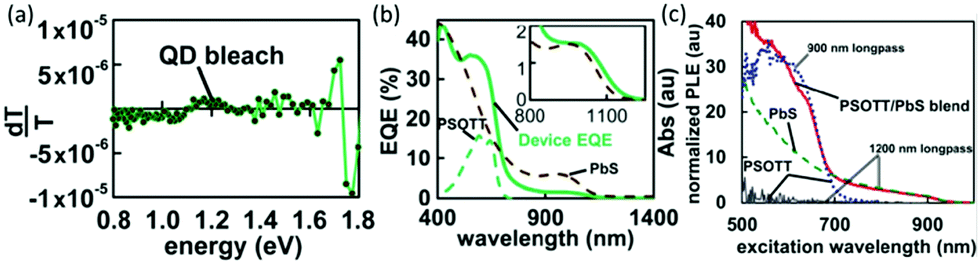 | ||
| Fig. 5 (a) In-phase signal from PIA for quantum dot/PSOTT blends. Absorption at the pump frequency was 0.258. The polaron feature is absent for the PSOTT/PbS blend, suggesting that upon excitation no significant charge transfer takes place between this polymer and the quantum dot. (b) EQE device data (solid line) overlaid with absorption data (dashed lines) for PSOTT/PbS film. (c) Photoluminescence excitation data. The red (solid) line is the signal from light detected at wavelengths greater than 1200 nm for PSOTT blended with PbS. The blue (dotted) line is the signal from light detected at wavelengths greater than 900 for pristine PSOTT. The green (dashed) line is the signal from light from neat PbS detected at wavelengths greater than 1200 nm. The gray (thin solid) line shows that no signal is detected from pristine PSOTT at wavelengths greater than 1200 nm. Reproduced with permission from ref. 68. Copyright 2013, Royal Society of Chemistry. | ||
3.3 Hole transfer
Compared to ultrafast electron transfer, hole transfer from nanocrystals to polymer was demonstrated to be much slower on the time scale of nanoseconds, which allowed the diffusion of holes within the inorganic component to the interface.67 Therefore, the hole transfer yield was largely unaffected by the polymer/nanocrystals ratio. Dowland et al. investigated the relationship between morphology and the charge transfer of hybrid films containing P3HT and in situ grown CdS.56 The nanoscale morphology of the hybrid films was controlled by adjusting the CdS content. As shown in Fig. 6a–c, an increase of CdS content led to smaller P3HT domains and larger CdS domains. Based on the absorption spectra, an excitation wavelength of 355 nm was used to generate electron–hole pairs primarily in CdS and 550 nm was used to generate excitons solely in P3HT. When P3HT was excited at 550 nm, hole-polaron signals of P3HT increased as the CdS content increased. In contrast, the hole-polaron signals of P3HT kept nearly constant when CdS was excited at 355 nm, which indicated that the hole transfer yield was independent of the nanoscale morphology. This phenomenon was also observed in aqueous-solution-processed poly(methoxy-phenylenevinylene) (MPPV)–CdTe hybrid films.63 Elevating the annealing temperature increased the length scale of phase segregation, while the hole transfer from CdTe nanocrystals to MPPV exhibited hardly any change.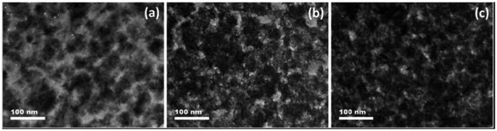 | ||
| Fig. 6 Bright field transmission electron microscopy images of CdS:P3HT blends obtained at 30% CdS (a), 50% CdS (b) and 70% CdS (c) volume fractions. Reproduced with permission from ref. 56. Copyright 2013, Royal Society of Chemistry. | ||
Similar to electron transfer, the hole transfer yield was correlated intimately with the energy difference between the HOMO level of polymer and the VB of nanocrystals. The hole transfer from CdTe nanocrystals to PPV and its derivatives was investigated using transient absorption spectra (Fig. 7a).63 When the VB of CdTe nanocrystals was fixed, introduction of alkoxy group shifted upwards the HOMO level of the polymer, thus increasing the energy difference. In comparison with the reference quartz/CdTe, the transient absorption decay spectra of the hybrid films exhibited accelerated decay rate, which indicated the occurrence of hole transfer from the CdTe nanocrystals to the polymer. Besides, the accelerated decay rate after introduction of alkoxy group implied increased hole transfer yield. Therefore, the hole transfer from CdTe nanocrystals to PPV or MPPV should be incomplete, which was investigated by the transient photovoltage. As shown in Fig. 7b, the transient photovoltage curves can be divided into two parts: charge separation and recombination. For the charge recombination region, the MPPV–CdTe hybrid initially overlapped with CdTe nanocrystals and then displayed a slower decay rate. The overlapped region was assigned to the recombination between holes and electrons on CdTe nanocrystals while the rest of the region was assigned to the recombination between holes on MPPV and electrons on CdTe nanocrystals.
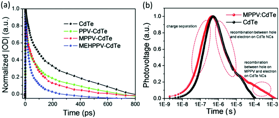 | ||
| Fig. 7 (a) Transient absorption decay kinetics of CdTe nanocrystals and polymer–CdTe nanocrystal films on a quartz substrate excited at 800 nm and probed at 825 nm. (b) Transient photovoltage responses of CdTe nanocrystals and MPPV:CdTe hybrid. Reproduced with permission from ref. 63 and 66. Copyright 2016 and 2015, Royal Society of Chemistry. | ||
3.4 Charge transport
Compared with PSCs, the difference of charge transport in HSCs is related to both polymer and nanocrystals. Different from polymer–fullerene systems, HSCs with high PCE were usually obtained with low polymer content (lower than 5%).52 The low polymer content will generate small polymer domains and severely influence their connectivity,56 thus reducing the ability of transporting holes in the polymer. This limited the thickness of active layer in HSCs to be about 100 nm, which was lower than that of nanocrystal solar cells and partial PSCs. As demonstrated in thin-film nanocrystal solar cells, nanocrystals can transport both holes and electrons.74 This avoided the waste of energy though the hole transfer was incomplete between the nanocrystals and polymers. Additionally, the existence of trap states on nanocrystals greatly influenced the charge transport and recombination.69–71 Therefore, a lot of work about passivating traps by ligand exchange has been done to improve the performance of HSCs.3.5 The essence of working junction
Based on the staggered band alignment and similarity to polymer–fullerene solar cells, type-II heterojunction was primarily believed to govern the working principle of HSCs.11 In this case, the open-circuit voltage (Voc) should be determined by the energy difference between the CB of the nanocrystals and the HOMO level of the polymer. However, a few works in recent years reported that the working principle of HSCs may not be type-II junction.52,60–62 For example, You et al. investigated the relationship between Voc and HOMO level of polymers in GaAs/polymer planar heterojunction (PHJ) solar cells.60 In their study, a series of semiconducting polymers with different HOMO level were selected and the CB of GaAs wafer was fixed. Their result showed that the Voc was fixed around 0.6 V which was independent of the HOMO level of the polymer. Therefore, the authors concluded that the Schottky junction between GaAs and anode instead of type II heterojunction between polymer and GaAs determined the operation mechanism. A similar phenomenon was also observed in polymer–PbSe PHJ solar cells.61 In addition to the same Voc of HSCs based on polymers with different HOMO level, the Voc of HSCs was found to show a great improvement compared to that of PbSe Schottky junction solar cells. This was attributed to the formation of an interface dipole between polymer and PbSe nanocrystals and the direction of the interface dipole was consistent with the built-in potential. In addition to the PHJ, the same question was also investigated in BHJ HSCs.62 Chen et al. fabricated aqueous-solution-processed HSCs from a series of water-soluble polymers with different HOMO level and nanocrystals with different Fermi level.63 When the CB of nanocrystals was fixed, changing the HOMO level of the polymer led to hardly any variation in Voc. Nevertheless, when the Fermi level of the cathode was fixed, changing the Fermi level of the nanocrystals changed the difference between nanocrystals and cathode, thus changing Voc. Therefore, the working principle of aqueous-solution-processed HSCs followed the p–n junction instead of type-II heterojunction. Likewise, the function of the polymer was to provide an interface dipole and to transport holes.It is worth noting that the above-mentioned results were obtained for PHJ or BHJ with high weight ratio of nanocrystals (higher than 90%). Yang et al. reported that the Schottky junction formed between fullerene and anode dominated the operation principle in PSCs when the relative amount of polymer was low (5%).75Voc was determined by the difference between the Fermi level of fullerene and the anode. In this case, the PSCs were very similar to the HSCs. The fullerenes or nanocrystals contribute mainly to the photo-absorption, while the polymers mainly function as hole acceptors and transporters. Subsequently, they reported that the Schottky junction transformed to a BHJ when increasing the content of polymer and Voc was determined by the difference between the HOMO level of polymer and LUMO level of fullerene.76
Since different optimization strategies may be adopted, it is required to elucidate the essence of the junction in HSCs. Whether the working junction of HSCs with high content of nanocrystal is a p–n junction or a Schottky junction should be confirmed in more systems. The relationship between polymer/nanocrystals ratio and Voc should also be further investigated.
4. Improvement of HSCs
In recent years, the PCE of HSCs has been progressively increased to 6%. The improvement of device performance mainly originates from suitable ligand exchange and optimization of device structure.4.1 Improving performance by ligand exchange
In a typical synthesis based on organic solvent, long-chain organic ligands are used to stabilize the nanocrystals, thus making the nanocrystals solution-processable.11 However, the existence of long-chain ligands will increase the nanocrystals/nanocrystals and polymer/nanocrystals distance, which will hinder charge transfer and transport.12 Besides, the bare atoms on the surface of nanocrystals may serve as trap states which may increase the possibility of non-radiative decay.77 Therefore, selecting suitable short-chain ligands to replace the long-chain ligands and passivate the trap states is important to achieve efficient HSCs.In the early work on HSCs, pyridine and short-chain amines were usually used for ligand exchange.14,21 However, these ligands cannot effectively passivate the surface trap states and completely remove the long-chain ligands, thus leading to most of the HSCs showing PCE of lower than 4%. In more recent years, PbS nanocrystal solar cells developed rapidly with PCE exceeding 11% which primarily benefited from effective trap passivation by ligand exchange.78 These ligands included ethanedithiol (EDT), benzenedithiol (BDT), 3-mercaptopropionic acid (MPA) and inorganic ligands, such as cetyltrimethylammonium bromide (CTAB), tetrabutylammonium iodide (TBAI), iodine, PbI2etc.77,79 This provided instructive guidelines for optimization of HSCs. For example, Ren et al. reported the first HSCs with PCE exceeding 4% based on P3HT nanowires and CdS nanocrystals treated by EDT.80 Subsequently, Zhou et al. transferred this method to CdSe nanorods and a low-bandgap polymer and obtained PCE approaching 5%.64 As shown in Fig. 8, EDT treatment resulted in removal of charged ligands and formation of Cd–thiolate on CdSe nanocrystal surface. The effective removal of organic ligands from the CdSe nanorod surface after EDT treatment was confirmed by infrared absorption, NMR, and X-ray photoelectron spectroscopies. The efficiency increase can be attributed to the reduction in charge recombination sites on the nanocrystal surface and the simultaneous increase in electron transport. Compared with EDT, BDT was more appealing due to the existence of conjugated aromatic ring. Fu et al. investigated the relationship between position of mercapto groups on BDT and device performance of polymer/CdSe HSCs.81 As shown in Fig. 9, highest PCE of 4.18% was achieved by attaching BDT in the “face-on” geometry on the surface of CdSe nanocrystals. The “face-on” geometry minimized the nanocrystal/nanocrystal and polymer/nanocrystal distance. Furthermore, the “electroactive” π-orbitals of BDT were expected to further enhance the electronic coupling of nanocrystal/nanocrystal and polymer/nanocrystal, thus facilitating charge transfer and transport.
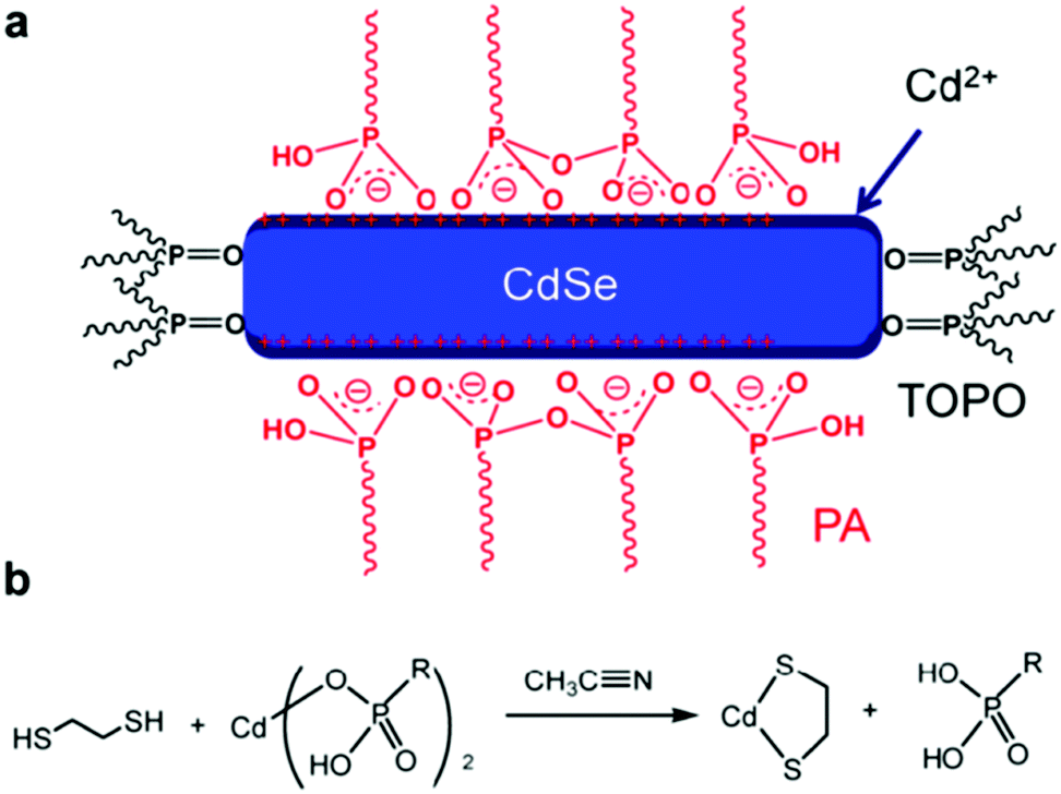 | ||
| Fig. 8 Proposed cleavage mechanism of phosphonic acids (X-type ligands) upon EDT treatment. (a) Schematic illustration of surface chemistry of colloidally synthesized CdSe nanorods. TOPO: trioctylphosphine oxide; PA: phosphonic acid. (b) Proposed cleavage mechanism of PA molecules from nanocrystals upon EDT treatment. Reproduced with permission from ref. 64. Copyright 2013, American Chemical Society. | ||
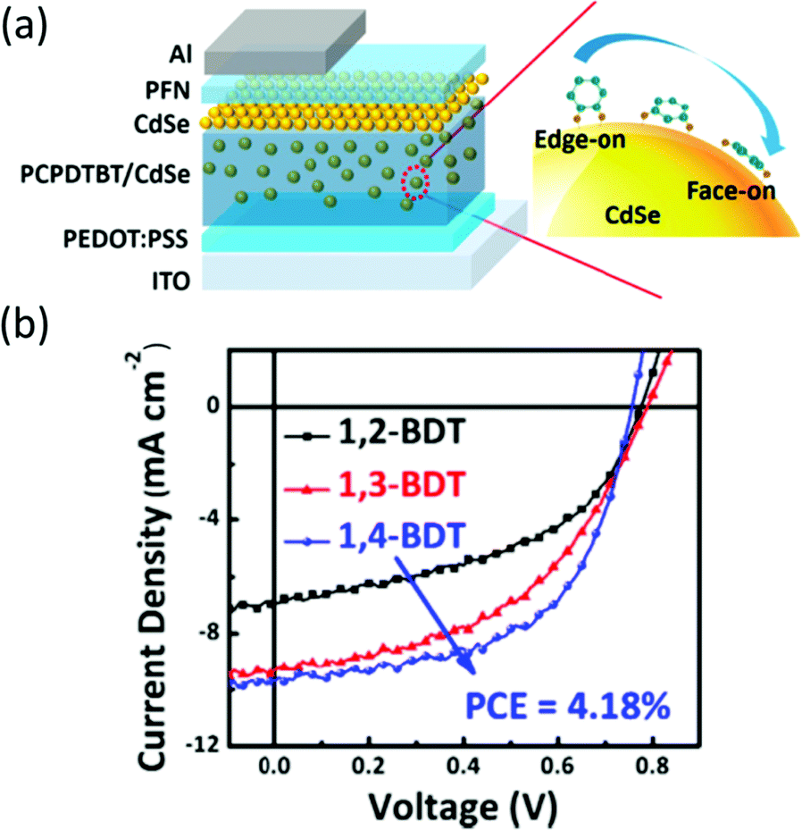 | ||
| Fig. 9 (a) Schematic device structure and schematic illustration of orientation of various benzenedithiols on the surface of CdSe QDs. (b) J–V characteristics of PCPDTBT/CdSe QDs HSCs with various orientated benzenedithiols at polymer/nanocrystal interface under simulated 1 Sun AM 1.5 solar illumination. Reproduced with permission from ref. 81. Copyright 2014, American Chemical Society. | ||
In PbS nanocrystal solar cells, the device performance with different ligand exchange strategies increased as follows: inorganic ligand > MPA > EDT. Colbert et al. introduced these ligand exchange methods into polymer–PbS nanocrystal HSCs and compared corresponding device performance.82 In their work, HSCs treated with MPA showed increased PCE than HSCs treated with EDT, which was similar to that of PbS nanocrystal solar cells. In contrast, HSCs treated with TBAI showed obviously decreased Voc, fill factor (FF) and PCE. The authors claimed that the decreased device performance was correlated with decreased carrier lifetime and increased carrier recombination rate, which was confirmed by PIA and transient photovoltage characterizations. However, the work reported by Zhang et al. showed different results.83 In that work, PHJ HSCs were fabricated from P3HT and PbSe nanocrystals. EDT and CTAB were used for ligand exchange, respectively. They found the mobility of PbSe nanocrystals treated by CTAB was much higher than that of PbSe nanocrystals treated by EDT. Therefore, the HSCs with CTAB treatment showed higher PCE. This result was consistent with the rule in PbS nanocrystal solar cells. The different results in these two works may be due to different device structure. In general, replacing long-chain ligands with short-chain ones will reduce the film volume, which can lead to film cracking and leakage current. It has been demonstrated that the ligand exchange was incomplete when using MPA or EDT. While for TBAI and CTAB, ligand exchange was nearly complete, which may lead to more film cracking and leakage current. But this question could be overcome in the PHJ structure as the double-layer fabrication process could effectively block cracking in the film and thus lower the leakage current.
The above-mentioned ligand exchange strategies were all conducted after deposition of thin film, which may have several inherent drawbacks: (i) ligand exchange can be impeded by slow and/or incomplete solid-state ligand diffusion through the BHJ film, (ii) reduction of the film volume through exchange of small ligands for large ones can lead to film cracking, and (iii) the dip washing process used for thin-film ligand exchange can lead to a low ligand exchange efficiency. In this regard, Lu et al. proposed a novel one-step colloidal ligand exchange process for PbS nanocrystals.84 In their design, lead iodide and n-butylamine were used for ligand exchange before film deposition. The simultaneous use of two ligands makes PbS nanocrystals colloidally stable and compatible with polymer in the same solvent. Time-resolved photoluminescence and transient absorption spectroscopies confirmed efficient charge transfer between PbS nanocrystals and polymer, which led to efficient HSCs with PCE of 4.8%.
At present, it is still challenging to promote HSCs by directly imitating the strategies demonstrated to be successful in PbS nanocrystal solar cells. This should be attributed to the more complex characteristic of HSCs compared to PbS nanocrystal solar cells. Therefore, much attention should be devoted to investigate the difference between HSCs and PbS nanocrystal solar cells when treated with the same ligands, especially the difference in carrier dynamics, including density of trap states, charge transport, recombination, etc.
When synthesizing the aqueous nanocrystals, short thiol ligands were usually selected as the stabilizer,85 which eliminated the requirement of the ligand exchange process for application in photovoltaics. Yu et al. reported the fabrication of aqueous-solution-processed HSCs based on PPV precursor and CdTe nanocrystals. The as-synthesized CdTe nanocrystals were stabilized by mercaptoethylamine (MA).86 MA may serve as a hole trap due to the existence of amine group. Therefore, the removal of MA ligands by thermal treatment was required to obtain efficient devices. On the other hand, thermal treatment promoted the conversion of PPV precursor to PPV and the growth of CdTe nanocrystals.87,88 In this work, a PCE of 2.14% was obtained, which was the highest for solar cells based on water-soluble material at that time.
As mentioned above, the function of ligands is to bind with the atoms on the surface of nanocrystals to reduce the dangling bonds, which are the origin of trap states. Therefore, the removal of MA ligands after annealing may generate a large amount of trap states. In a recent work, Zeng et al. discovered that this problem could be effectively solved after incorporating CdTe nanocrystals with chlorine (Cl) ions.89 The Cl ions were introduced during the synthetic process. The residual Cl after annealing functions as a ligand binding on the CdTe nanocrystal surface to reduce the surface trap states. This was similar to the functions of atomic ligands (Cl, Br, I) in PbS nanocrystal solar cells.77 In addition, it was demonstrated that the Cl in as-prepared nanocrystals can promote crystal growth in a sintering process to reduce the grain boundaries (Fig. 10a–c). These two aspects led to reduced nongeminate recombination (including bimolecular recombination (Fig. 10e) and trap-assisted recombination (Fig. 10f)) and improved charge extraction efficiency after incorporating CdTe nanocrystals with Cl, thus dramatically improving the device performance. As shown in Fig. 10d, a best PCE of 5.25% was achieved through optimizing the Cl content in as-prepared CdTe nanocrystals. Besides, the authors noted that though the residual Cl after annealing could effectively passivate the surface trap states, the trap-assisted recombination was not entirely suppressed for the HSCs based on CdTe nanocrystals with the optimal Cl content. This indicated that the surfaces of CdTe nanocrystals are still imperfectly passivated. Therefore, the photovoltaic performance of aqueous-processed CdTe-based HSCs can be improved through adopting improved passivation methods to reduce the trap states on the surface of nanocrystals in future work.
 | ||
| Fig. 10 TEM images of PPV/CdTe hybrid films based on (a) 0 mM and (b) 60 mM. (c) XRD patterns of CdTe NCs with and without Cl annealed at 350 °C. (d) The corresponding J–V characteristics measured under 100 mW cm−2 AM 1.5G illumination, (e) the measured Jsc and (f) Voc of the HSCs as a function of light intensity (symbols), together with linear fits to Jsc and Voc data (solid lines). Adapted and reproduced with permission from ref. 89. Copyright 2017, Wiley-VCH. | ||
4.2 Improving performance by optimizing device structure
In addition to the use of new ligand exchange strategies, novel device architectures have also been adopted in HSCs to further increase the PCE. Liu et al. reported that efficient polymer–PbSxSe1−x nanocrystal HSCs benefited from vertical phase segregation.52 As shown in Fig. 11, after the formation of self-assembled vertical phase segregation in the blend layer, a pure nanocrystal layer was deposited on top of the blend film to form the desired D–D:A–A vertical structure. The bottom polymer-rich and upper nanocrystal-rich layers facilitated carrier transport, and functioned as electron and hole blocking layers respectively. Therefore, a record-high PCE of 5.50% and a maximum FF of 67% were achieved for such type of HSCs. This structure was also applied in HSCs based on CdSe nanocrystals and PCE of about 4% could be obtained.85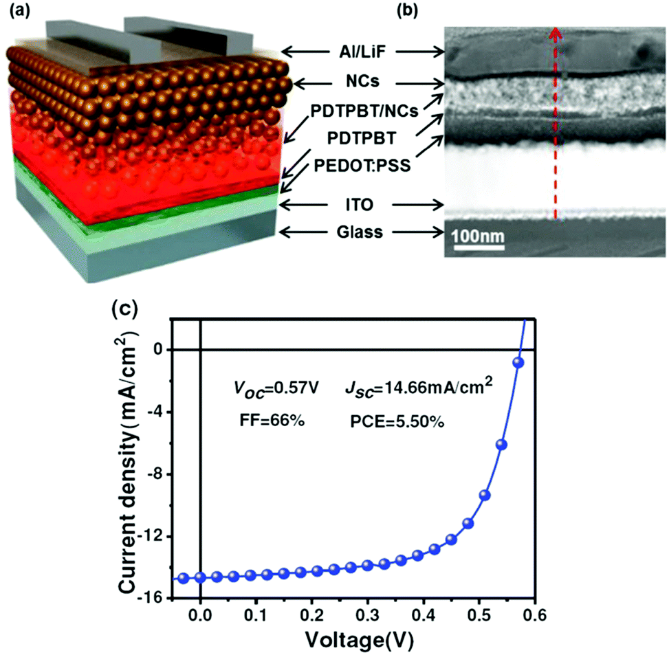 | ||
| Fig. 11 (a) Schematic diagram of the hybrid photovoltaic device used in this study, showing a vertical D–D:A–A structure in the active film. Self-assembled vertical phase separation occurs in the polymer/NC blend film during spin-coating. Then pure NC layers are deposited on top of the blend layer, leading to the formation of the desired D–D:A–A structure. (b) Cross-sectional HAADF-STEM image of the same device. (c) J–V curve and photovoltaic parameters of the optimized solar cell device. Reproduced with permission from ref. 52. Copyright 2013, Wiley-VCH. | ||
The ordered heterojunction (OHJ) concept has been established on the basis of BHJ with the donor and acceptor domains being perpendicular to the substrate. OHJ can effectively decrease the occurrence of isolated domains and charge transport distance before reaching the electrodes. Therefore, the OHJ structure is expected to show superior device performance. Liu et al. constructed OHJ HSCs based on ZnO nanorod arrays (ZCS-NA) and obtained PCE as high as 5.01%.65 As shown in Fig. 12, ZCS-NA were firstly grown on an ITO substrate via a hydrothermal method. After that, CdS/Sb2S3 shell was deposited with the ZCS-NA as template. Doped poly(2-methoxy-5-(2-ethylhexyloxy)-1,4-phenylenevinylene) (MEH-PPV) with high hole mobility was used to accept and transport holes. This ordered structure greatly reduced the carrier recombination during carrier transport.
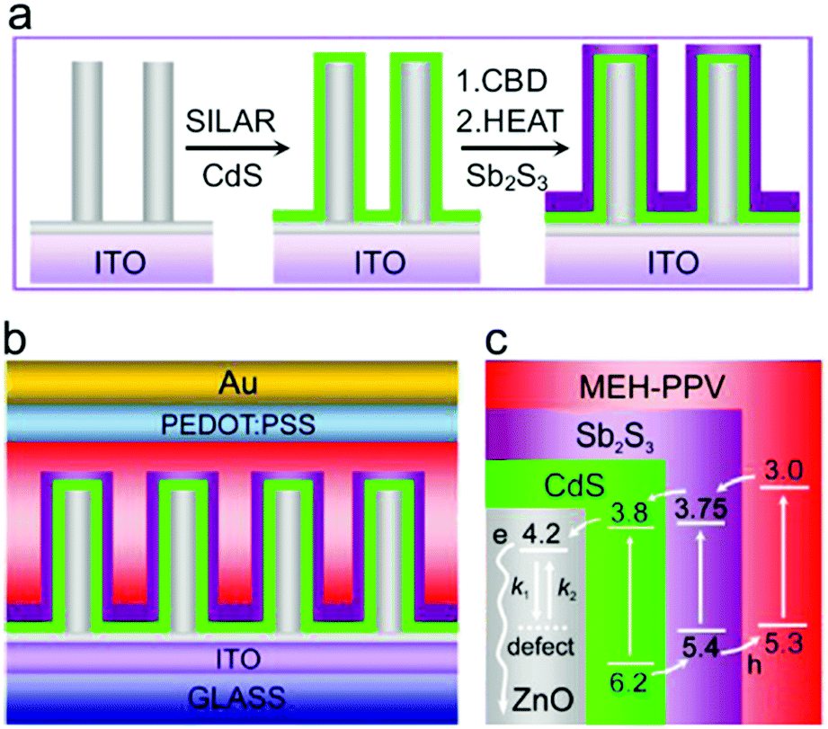 | ||
| Fig. 12 (a) Synthesis of ZCS-NA. (b) Architecture in MEH-PPV/ZCS-NA solar cells. (c) Band level (eV) alignments in the solar cells, where the arrows show the charge transfer of electrons and holes. Surface defects on ZnO nanorods can influence electron transport by trapping (k1) and detrapping (k2) processes. Reproduced with permission from ref. 65. Copyright 2015, Elsevier. | ||
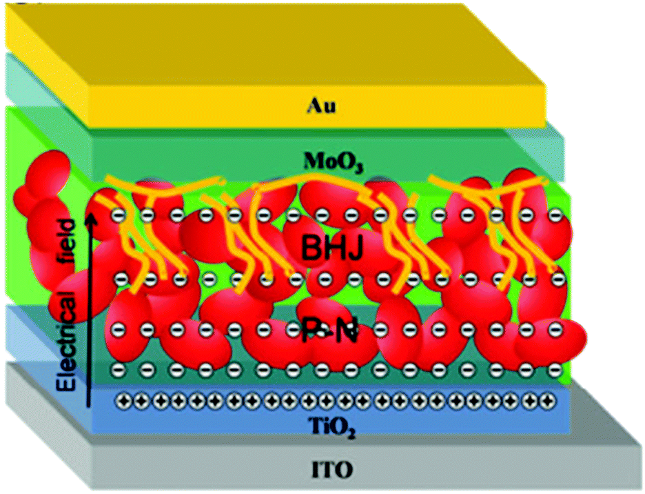
Similar to organic-solvent-processed HSCs, the improvement of aqueous-solution-processed HSCs was mainly from optimization of device structure. The aqueous-solution-processed HSCs were initially based on the normal structure in which PEDOT:PSS was selected as the hole transport layer. The PEDOT:PSS layer will be partly dissolved when the aqueous active layer is spin-coated, as PEDOT:PSS is a water-soluble polymer. As a consequence, the function of the PEDOT:PSS layer was weakened, leading to an increase of the leak current. As a result, Voc and FF remained relatively low.86 In order to solve this problem, Chen et al. proposed inverted devices with the configuration of ITO/TiO2/poly(1,4-naphthalenevinylene) (PNV):CdTe/MoO3/Au.90 As TiO2 showed sufficient water resistance, the leakage current was prohibited effectively. Compared to conventional solar cells, Voc and FF greatly increased, thus making an increased PCE of 3.61%.
The photoresponse range of HSCs was usually wider than that of PSCs, especially when nanocrystals with near infrared absorption were used. Nevertheless, HSCs did not exhibit obviously higher photocurrent than PSCs, due to the limited thickness of active layer. As the low content of polymer reduced the hole transport ability, a thicker active layer will lead to the accumulation of holes, which is detrimental to device performance. In this case, an active layer with vertical phase segregation was introduced, which balanced the photo-absorption and carrier transport.52,63,91 Optimizing the thickness of the active layer led to PCE of 5.41% which was comparable to that of the organic counterpart.52,63
In conventional solution processing, the polymer and nanocrystals were mixed before deposition. This process had two drawbacks: (i) the isolated polymer or nanocrystal phases may act as carrier traps, which can increase the carrier recombination; (ii) the annealing temperature of polymer and nanocrystals was identical, which means one cannot optimize properties of polymer and nanocrystals simultaneously. To overcome these two drawbacks, Du et al. developed a post-permeation method to construct a polymer–nanocrystal BHJ.92 As shown in Fig. 13, CdTe nanocrystals were first mixed with CTAB before spin-coating. When the film was annealed, the CTAB molecules volatilized, leaving lots of voids in the film. After that, a P3HT solution was spin-coated and the permeation of polymer led to the formation of BHJ structure. Isolated polymer or nanocrystal phases cannot be formed in this method. Besides, the hole transport layer can be omitted due to the formation of thin P3HT layer on the top surface of the blending layer. Through optimizing the annealing temperature of each of P3HT and CdTe nanocrystals, a champion PCE of 6.36% was obtained, which was one of the highest values of polymer–nanocrystal HSCs up to now.
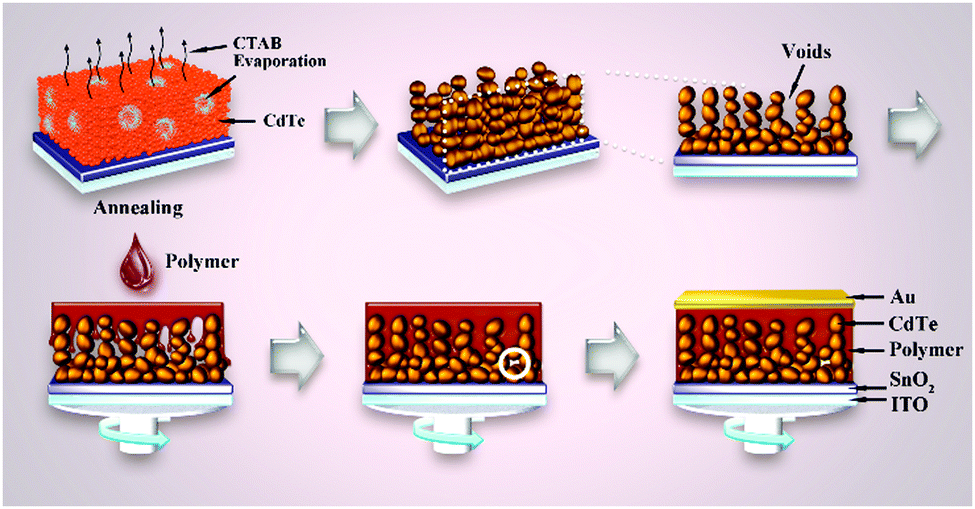 | ||
| Fig. 13 The process of void formation in the CdTe layer and the post-permeation of polymer into the CdTe layer as well as the final device structure. Reproduced with permission from ref. 92. Copyright 2017, Wiley-VCH. | ||
Up to now, the improvement of HSCs is mainly attributed to the optimization of device structure. The best structure is an active layer with vertical phase segregation (Fig. 14). This is reasonable due to the low polymer content and bipolar carrier transport of nanocrystals. The advantage of this structure will be strengthened when considering the formation of p–n junction or Schottky junction between nanocrystals and the electrode. In this case, a depletion region is established and carrier transport in the nanocrystal layer will be promoted by the electrical field. In the blending layer, the recombination loss will be reduced as a result of prolonged carrier lifetime induced by charge transfer.
 | ||
| Fig. 14 The proposed operation mechanism of HSCs with a vertical component distribution. Reproduced with permission from ref. 63. Copyright 2016, Royal Society of Chemistry. | ||
The selected performance parameters of high-efficiency HSCs based on conjugated polymer and nanocrystals are summarized in Table 1.
| Device structure | J sc (mA cm−2) | V oc (V) | FF | PCE | Published year | Ref. |
|---|---|---|---|---|---|---|
| ITO/PEDOT:PSS/P3HT:CdS/BCP/Mg/Ag | 10.9 | 1.1 | 0.35 | 4.1 | 2011 | 80 |
| ITO/PEDOT:PSS/PCPDTBT:CdSe NR/Al | 12.8 | 0.74 | 0.50 | 4.7 | 2013 | 64 |
| ITO/PEDOT:PSS/PCPDTBT:CdSe/CdSe/PFN/Al | 9.50 | 0.76 | 0.54 | 3.92 | 2014 | 81 |
| ITO/PEDOT:PSS/Si-PCPDTBT:PbS/ZnO/Al | 18.2 | 0.48 | 0.55 | 4.78 | 2016 | 84 |
| ITO/PEDOT:PSS/PDTPBT:PbSxSe1−x/PbSxSe1−x/LiF/Al | 14.66 | 0.57 | 0.66 | 5.50 | 2013 | 52 |
| ITO/ZnO/CdS/Sb2S3/MEH-PPV/PEDOT:PSS/Au | 13.53 | 0.73 | 0.508 | 5.01 | 2015 | 65 |
| ITO/TiO2/PNV:CdTe/MoO3/Au | 12.5 | 0.544 | 0.531 | 3.61 | 2013 | 90 |
| ITO/TiO2/CdTe/PPV:CdTe/MoO3/Au | 16.08 | 0.591 | 0.501 | 4.76 | 2013 | 91 |
| ITO/TiO2/CdTe/MPPV:CdTe/MoO3/Au | 15.15 | 0.624 | 0.548 | 5.18 | 2015 | 66 |
| ITO/TiO2/CdTe/PPV:CdTe/MoO3/Au | 18.4 | 0.657 | 0.447 | 5.41 | 2016 | 63 |
| ITO/TiO2/CdTe/PPV:CdTe/MoO3/Au | 17.3 | 0.595 | 0.502 | 5.25 | 2017 | 89 |
| ITO/SnO2/CdTe/CdTe:P3HT/P3HT/Au | 17.66 | 0.67 | 0.54 | 6.36 | 2017 | 92 |
5. Challenges and perspective
This article reviews the recent work concerning operation mechanism and performance optimization. This provides new understanding of HSCs, which is instructive for their future development. Though improved PCE has been achieved in recent years, continued device optimization is still imperative to meet the requirements of practical applications. At present, HSCs are facing challenges as follows:(1) The incomplete electron transfer from polymer to nanocrystals will cause a waste of light absorption by the polymer. This problem will be reduced with relatively high electron transfer yield when the polymer content is low. However, a low polymer content leads to small-sized polymer domains, which will influence the connectivity and hole mobility of polymer phase. As a consequence, the thickness of the active layer in BHJ structure is limited, thus causing incomplete photo-absorption yield.
(2) Passivating traps of nanocrystals by ligand exchange. The existence of traps on the surface of nanocrystals is detrimental for charge transfer and transport. It is still challenging to optimize HSCs by directly imitating the successful strategies used in PbS nanocrystal solar cells. More work should be done to clarify the underlying reasons by comparing the two kinds of solar cells with the same ligand treatment.
(3) The essence of the working junction should be investigated in more detail. Type-II heterojunction is primarily believed to be the working principle of HSCs, while recent reports show that a p–n or Schottky junction is the working junction of HSCs. Since different optimization strategies may be adopted, it is required to elucidate the essence of the junction in HSCs. Besides, whether the polymer/nanocrystal ratio will influence the essence of the junction should also be investigated.
When the challenges are overcome, it may be possible that the HSCs outperform the PSCs, considering the advantages of nanocrystals over fullerenes. Another problem for HSCs is the use of heavy metal-based nanocrystals, such as CdTe, CdSe and PbS. In this case, environmentally friendly materials, such as Cu2ZnSnS4, CuInS2 and carbon-based materials, should be used in HSCs.93,94 In view of environmentally friendly concept, aqueous-solution-processed HSCs are more appealing, especially in large-scale production processes. At present, the efficient aqueous-solution-processed HSCs are usually based on PPV. On the other hand, it seems that CdTe nanocrystals are the only option for efficient aqueous-solution-processed HSCs. Therefore, the available range polymers and nanocrystals should be broadened. The PCE of aqueous-solution-processed HSCs is comparable to that of organic counterparts. Besides, excellent long-term stability has been demonstrated for aqueous-solution-processed HSCs.51 These features reflect the promising potential of aqueous-solution-processed HSCs.
Acknowledgements
This work was financially supported by the National Science Foundation of China (NSFC) under grant no. 51433003, and the National Basic Research Program of China (973 Program) under grant no. 2014CB643503. The National key research and development program of China (2016YFB0401701).Notes and references
- S. Gunes, H. Neugebauer and N. S. Sariciftci, Chem. Rev., 2007, 107, 1324 CrossRef PubMed.
- X. Li, F. Xie, S. Zhang, J. Hou and W. C. H. Choy, Light: Sci. Appl., 2015, 4, e273 CrossRef CAS.
- Z. He, C. Zhong, S. Su, M. Xu, H. Wu and Y. Cao, Nat. Photonics, 2012, 6, 593 CrossRef CAS.
- B. C. Thompson and J. M. Frechet, Angew. Chem., Int. Ed., 2008, 47, 58 CrossRef CAS PubMed.
- F. C. Krebs, Sol. Energy Mater. Sol. Cells, 2009, 93, 394 CrossRef CAS.
- F. C. Krebs, Sol. Energy Mater. Sol. Cells, 2009, 93, 465 CrossRef CAS.
- S. E. Shaheen, R. Radspinner, N. Peyghambarian and G. E. Jabbour, Appl. Phys. Lett., 2001, 79, 2996 CrossRef CAS.
- S. S. Kim, S. I. Na, J. Jo, G. Tae and D. Y. Kim, Adv. Mater., 2007, 19, 4410 CrossRef CAS.
- Y. Liu, J. Zhao, Z. Li, C. Mu, W. Ma, H. Hu, K. Jiang, H. Lin, H. Ade and H. Yan, Nat. Commun., 2014, 5, 5293 CrossRef CAS PubMed.
- H. Kang, W. Lee, J. Oh, T. Kim, C. Lee and B. J. Kim, Acc. Chem. Res., 2016, 49, 2424 CrossRef CAS PubMed.
- F. Gao, S. Ren and J. Wang, Energy Environ. Sci., 2013, 6, 2020 CAS.
- Y. Zhou, F. S. Riehle, Y. Yuan, H.-F. Schleiermacher, M. Niggemann, G. A. Urban and M. Krüger, Appl. Phys. Lett., 2010, 96, 013304 CrossRef.
- Y. Zhou, M. Eck and M. Krüger, Energy Environ. Sci., 2010, 3, 1851 CAS.
- M. J. Greaney, S. Das, D. H. Webber, S. E. Bradforth and R. L. Brutchey, ACS Nano, 2012, 6, 4222 CrossRef CAS PubMed.
- N. C. Greenham, X. Peng and A. P. Alivisatos, Phys. Rev. B: Condens. Matter Mater. Phys., 1996, 54, 17628 CrossRef CAS.
- S. Dayal, M. O. Reese, A. J. Ferguson, D. S. Ginley, G. Rumbles and N. Kopidakis, Adv. Funct. Mater., 2010, 20, 2629 CrossRef CAS.
- K. F. Jeltsch, M. Schädel, J.-B. Bonekamp, P. Niyamakom, F. Rauscher, H. W. A. Lademann, I. Dumsch, S. Allard, U. Scherf and K. Meerholz, Adv. Funct. Mater., 2012, 22, 397 CrossRef CAS.
- S. Li, L. Ye, W. Zhao, S. Zhang, S. Mukherjee, H. Ade and J. Hou, Adv. Mater., 2016, 28, 9423 CrossRef CAS PubMed.
- W. Zhao, S. Li, S. Zhang, X. Liu and J. Hou, Adv. Mater., 2017, 29, 1604059 CrossRef PubMed.
- W. U. Huynh, J. J. Dittmer and A. P. Alivisatos, Science, 2002, 295, 2425 CrossRef CAS PubMed.
- I. Lokteva, N. Radychev, F. Witt, H. Borchert, J. Parisi and J. Kolny-Olesiak, J. Phys. Chem. C, 2010, 114, 12784 CAS.
- J. Seo, M. J. Cho, D. Lee, A. N. Cartwright and P. N. Prasad, Adv. Mater., 2011, 23, 3984 CrossRef CAS PubMed.
- J. Liu, T. Tanaka, K. Sivula, A. P. Alivisatos and M. J. Fréchet, J. Am. Chem. Soc., 2004, 126, 6550 CrossRef CAS PubMed.
- E. Arici, N. S. Sariciftci and D. Meissner, Adv. Funct. Mater., 2003, 13, 165 CrossRef CAS.
- B. Sun, E. Marx and N. C. Greenham, Nano Lett., 2003, 3, 961 CrossRef CAS.
- X. Chen, Q. Liu, Q. Wu, P. Du, J. Zhu, S. Dai and S. Yang, Adv. Funct. Mater., 2016, 26, 1719 CrossRef CAS.
- S. A. McDonald, G. Konstantatos, S. Zhang, P. W. Cyr, E. J. Klem, L. Levina and E. H. Sargent, Nat. Mater., 2005, 4, 138 CrossRef CAS PubMed.
- Q. Guo, S. J. Kim, M. Kar, W. N. Shafarman, R. W. Birkmire, E. A. Stach, R. Agrawal and H. W. Hillhouse, Nano Lett., 2008, 8, 2982 CrossRef CAS PubMed.
- P. A. van Hal, M. M. Wienk, J. M. Kroon, W. J. H. Verhees, L. H. Slooff, W. J. H. van Gennip, P. Jonkheijm and R. A. J. Janssen, Adv. Mater., 2003, 15, 118 CrossRef CAS.
- S. D. Oosterhout, M. M. Wienk, S. S. van Bavel, R. Thiedmann, L. J. Koster, J. Gilot, J. Loos, V. Schmidt and R. A. Janssen, Nat. Mater., 2009, 8, 818 CrossRef CAS PubMed.
- S. Yao, Z. Chen, F. Li, B. Xu, J. Song, L. Yan, G. Jin, S. Wen, C. Wang, B. Yang and W. Tian, ACS Appl. Mater. Interfaces, 2015, 7, 7146 CAS.
- Y. Wu and G. Zhang, Nano Lett., 2010, 10, 1628 CrossRef CAS PubMed.
- H. C. Chen, C. W. Lai, I. C. Wu, H. R. Pan, I. W. Chen, Y. K. Peng, C. L. Liu, C. H. Chen and P. T. Chou, Adv. Mater., 2011, 23, 5451 CrossRef CAS PubMed.
- G. Itskos, P. Papagiorgis, D. Tsokkou, A. Othonos, F. Hermerschmidt, S. P. Economopoulos, M. Yarema, W. Heiss and S. Choulis, Adv. Energy Mater., 2013, 3, 1490 CrossRef CAS.
- Y. Zhou, M. Eck, C. Veit, B. Zimmermann, F. Rauscher, P. Niyamakom, S. Yilmaz, I. Dumsch, S. Allard and U. Scherf, Sol. Energy Mater. Sol. Cells, 2011, 95, 1232 CrossRef CAS.
- H. Borchert, Energy Environ. Sci., 2010, 3, 1682 CAS.
- W. J. E. Beek, L. H. Slooff, M. M. Wienk, J. M. Kroon and R. A. J. Janssen, Adv. Funct. Mater., 2005, 15, 1703 CrossRef CAS.
- J.-F. Lin, W.-C. Yen, C.-Y. Chang, Y.-F. Chen and W.-F. Su, J. Mater. Chem. A, 2013, 1, 665 CAS.
- T. Xu and Q. Qiao, Energy Environ. Sci., 2011, 4, 2700 CAS.
- I. Gur, N. A. Fromer, C.-P. Chen, A. G. Kamaras and A. P. Alivisatos, Nano Lett., 2007, 7, 409 CrossRef CAS PubMed.
- Y. X. Nan, X. L. Hu, T. T. Larsen-Olsen, B. Andreasen, T. Tromholt, J. W. Andreasen, D. M. Tanenbaum, H. Z. Chen and F. C. Krebs, Nanotechnology, 2011, 22, 475301 CrossRef PubMed.
- T. R. Andersen, T. T. Larsen-Olsen, B. Andreasen, A. P. L. Böttiger, J. E. Carlé, M. Helgesen, E. Bundgaard, K. Norrman, J. W. Andreasen, M. Jørgensen and F. C. Krebs, ACS Nano, 2011, 5, 4188 CrossRef CAS PubMed.
- W. Cao, X. Zhang, X. Miao, Z. Yang and H. Xu, Angew. Chem., Int. Ed., 2013, 52, 6233 CrossRef CAS PubMed.
- F. Huang, H. Wu and Y. Cao, Chem. Soc. Rev., 2010, 39, 2500 RSC.
- Z. He, C. Zhong, X. Huang, W. Y. Wong, H. Wu, L. Chen, S. Su and Y. Cao, Adv. Mater., 2011, 23, 4636 CrossRef CAS PubMed.
- R. Søndergaard, M. Helgesen, M. Jørgensen and F. C. Krebs, Adv. Energy Mater., 2011, 1, 68 CrossRef.
- H. Wei, G. Jin, L. Wang, L. Hao, T. Na, Y. Wang, W. Tian, H. Sun, H. Zhang, H. Wang, H. Zhang and B. Yang, Adv. Mater., 2014, 26, 3655 CrossRef CAS PubMed.
- G. Jin, Z. Chen, C. Dong, Z. Cheng, X. Du, Q. Zeng, F. Liu, H. Sun, H. Zhang and B. Yang, ACS Appl. Mater. Interfaces, 2016, 8, 7101 CAS.
- Q. Zeng, Z. Chen, Y. Zhao, X. Du, F. Liu, G. Jin, F. Dong, H. Zhang and B. Yang, ACS Appl. Mater. Interfaces, 2015, 7, 23223 CAS.
- X. Du, Z. Chen, Z. Li, H. Hao, Q. Zeng, C. Dong and B. Yang, Adv. Energy Mater., 2014, 4, 1400135 CrossRef.
- Y. Zhao, Q. Zeng, X. Liu, S. Jiao, G. Pang, X. Du, K. Zhang and B. Yang, J. Mater. Chem. A, 2016, 4, 11738 CAS.
- Z. Liu, Y. Sun, J. Yuan, H. Wei, X. Huang, L. Han, W. Wang, H. Wang and W. Ma, Adv. Mater., 2013, 25, 5772 CrossRef CAS PubMed.
- M. J. Greaney and R. L. Brutchey, Mater. Today, 2015, 18, 31 CrossRef CAS.
- Z. Ning, O. Voznyy, J. Pan, S. Hoogland, V. Adinolfi, J. Xu, M. Li, A. R. Kirmani, J. P. Sun, J. Minor, K. W. Kemp, H. Dong, L. Rollny, A. Labelle, G. Carey, B. Sutherland, I. Hill, A. Amassian, H. Liu, J. Tang, O. M. Bakr and E. H. Sargent, Nat. Mater., 2014, 13, 822 CrossRef CAS PubMed.
- S. W. Tsang, H. Fu, R. Wang, J. Lu, K. Yu and Y. Tao, Appl. Phys. Lett., 2009, 95, 183505 CrossRef.
- S. A. Dowland, L. X. Reynolds, A. MacLachlan, U. B. Cappel and S. A. Haque, J. Mater. Chem. A, 2013, 1, 13896 CAS.
- S. D. Oosterhout, L. J. A. Koster, S. S. van Bavel, J. Loos, O. Stenzel, R. Thiedmann, V. Schmidt, B. Campo, T. J. Cleij, L. Lutzen, D. Vanderzande, M. M. Wienk and R. A. J. Janssen, Adv. Energy Mater., 2011, 1, 90 CrossRef CAS.
- E. Couderc, M. J. Greaney, R. L. Brutchey and S. E. Bradforth, J. Am. Chem. Soc., 2013, 135, 18418 CrossRef CAS PubMed.
- W. Guo, J. Yuan, H. Yuan, F. Jin, L. Han, C. Sheng, W. Ma and H. Zhao, Adv. Funct. Mater., 2016, 26, 713 CrossRef CAS.
- L. Yan and W. You, ACS Nano, 2013, 7, 6619 CrossRef CAS PubMed.
- Y. Sun, Z. Liu, J. Yuan, J. Chen, Y. Zhou, X. Huang and W. Ma, Org. Electron., 2015, 24, 263 CrossRef CAS.
- R. Mastria, A. Rizzo, C. Giansante, D. Ballarini, L. Dominici, O. Inganäs and G. Gigli, J. Phys. Chem. C, 2015, 119, 14972 CAS.
- Z. Chen, X. Du, G. Jin, Q. Zeng, F. Liu and B. Yang, Phys. Chem. Chem. Phys., 2016, 18, 15791 RSC.
- R. Zhou, R. Stalder, D. Xie, W. Cao, Y. Zheng, Y. Zhang, M. Plaisant, P. H. Holloway, K. S. Schanze, J. R. Reynolds and J. Xue, ACS Nano, 2013, 7, 4846 CrossRef CAS PubMed.
- C. Liu, Z. Qiu, F. Li, W. Meng, W. Yue, F. Zhang, Q. Qiao and M. Wang, Nano Energy, 2015, 12, 686 CrossRef CAS.
- Z. Chen, F. Liu, Q. Zeng, Z. Cheng, X. Du, G. Jin, H. Zhang and B. Yang, J. Mater. Chem. A, 2015, 3, 10969 CAS.
- U. B. Cappel, S. A. Dowland, L. X. Reynolds, S. Dimitrov and S. A. Haque, J. Phys. Chem. Lett., 2013, 4, 4253 CrossRef CAS PubMed.
- E. Strein, A. Colbert, S. Subramaniyan, H. Nagaoka, C. W. Schlenker, E. Janke, S. A. Jenekhe and D. S. Ginger, Energy Environ. Sci., 2013, 6, 769 CAS.
- M. L. Böhm, R. J. P. Kist, F. S. F. Morgenstern, B. Ehrler, S. Zarra, A. Kumar, Y. Vaynzof and N. C. Greenham, Adv. Energy Mater., 2014, 4, 1400139 CrossRef.
- Z. Li, W. Wang, N. C. Greenham and C. R. McNeill, Phys. Chem. Chem. Phys., 2014, 16, 25684 RSC.
- F. Gao, Z. Li, J. Wang, A. Rao, I. A. Howard, A. Abrusci, S. Massip, C. R. McNeill and N. C. Greenham, ACS Nano, 2014, 8, 3213 CrossRef CAS PubMed.
- Z. Fan, H. Zhang, W. Yu, Z. Xing, H. Wei, Q. Dong, W. Tian and B. Yang, ACS Appl. Mater. Interfaces, 2011, 3, 2919 CAS.
- L. Wang, H.-Y. Wang, H.-T. Wei, H. Zhang, Q.-D. Chen, H.-L. Xu, W. Han, B. Yang and H.-B. Sun, Adv. Energy Mater., 2014, 4, 1301882 CrossRef.
- J. Tang and E. H. Sargent, Adv. Mater., 2011, 23, 12 CrossRef CAS PubMed.
- B. Yang, F. Guo, Y. Yuan, Z. Xiao, Y. Lu, Q. Dong and J. Huang, Adv. Mater., 2013, 25, 572 CrossRef CAS PubMed.
- B. Yang, Z. Xiao and J. Huang, Appl. Phys. Lett., 2014, 104, 143304 CrossRef.
- J. Tang, K. W. Kemp, S. Hoogland, K. S. Jeong, H. Liu, L. Levina, M. Furukawa, X. Wang, R. Debnath, D. Cha, K. W. Chou, A. Fischer, A. Amassian, J. B. Asbury and E. H. Sargent, Nat. Mater., 2011, 10, 765 CrossRef CAS PubMed.
- M. Liu, O. Voznyy, R. Sabatini, F. P. Garcia de Arquer, R. Munir, A. H. Balawi, X. Lan, F. Fan, G. Walters, A. R. Kirmani, S. Hoogland, F. Laquai, A. Amassian and E. H. Sargent, Nat. Mater., 2017, 16, 258 CrossRef CAS PubMed.
- K. S. Jeong, J. Tang, H. Liu, J. Kim, A. W. Schaefer, K. Kemp, L. Levina, X. Wang, S. Hoogland, R. Debnath, L. Brzozowski, E. H. Sargent and J. B. Asbury, ACS Nano, 2012, 6, 89 CrossRef CAS PubMed.
- S. Ren, L. Y. Chang, S. K. Lim, J. Zhao, M. Smith, N. Zhao, V. Bulovic, M. Bawendi and S. Gradecak, Nano Lett., 2011, 11, 3998 CrossRef CAS PubMed.
- W. Fu, L. Wang, Y. Zhang, R. Ma, L. Zuo, J. Mai, T. K. Lau, S. Du, X. Lu, M. Shi, H. Li and H. Chen, ACS Appl. Mater. Interfaces, 2014, 6, 19154 CAS.
- A. E. Colbert, W. Wu, E. M. Janke, F. Ma and D. S. Ginger, J. Phys. Chem. C, 2015, 119, 24733 CAS.
- X. Zhang, Y. Zhang, H. Wu, L. Yan, Z. Wang, J. Zhao, W. W. Yu and A. L. Rogach, RSC Adv., 2016, 6, 17029 RSC.
- H. Lu, J. Joy, R. L. Gaspar, S. E. Bradforth and R. L. Brutchey, Chem. Mater., 2016, 28, 1897 CrossRef CAS.
- W. Fu, L. Wang, J. Ling, H. Li, M. Shi, J. Xue and H. Chen, Nanoscale, 2014, 6, 10545 RSC.
- W. Yu, H. Zhang, Z. Fan, J. Zhang, H. Wei, D. Zhou, B. Xu, F. Li, W. Tian and B. Yang, Energy Environ. Sci., 2011, 4, 2831 CAS.
- Z. Chen, H. Zhang, Z. Xing, J. Hou, J. Li, H. Wei, W. Tian and B. Yang, Sol. Energy Mater. Sol. Cells, 2013, 109, 254 CrossRef CAS.
- Z. Chen, Q. Zeng, F. Liu, G. Jin, X. Du, J. Du, H. Zhang and B. Yang, RSC Adv., 2015, 5, 74263 RSC.
- Q. Zeng, Z. Chen, F. Liu, G. Jin, X. Du, T. Ji, Y. Zhao, Y. Yue, H. Wang, D. Meng, T. Xie, H. Zhang and B. Yang, Sol. RRL, 2017, 1, 1600020 CrossRef.
- Z. Chen, H. Zhang, W. Yu, Z. Li, J. Hou, H. Wei and B. Yang, Adv. Energy Mater., 2013, 3, 433 CrossRef CAS.
- Z. Chen, H. Zhang, X. Du, X. Cheng, X. Chen, Y. Jiang and B. Yang, Energy Environ. Sci., 2013, 6, 1597 CAS.
- X. Du, Q. Zeng, G. Jin, F. Liu, T. Ji, Y. Yue, Y. Yang, H. Zhang and B. Yang, Small, 2017, 1603771 CrossRef PubMed.
- J. Zhong, Z. Xia, C. Zhang, B. Li, X. Liu, Y.-B. Cheng and J. Tang, Chem. Mater., 2014, 26, 3573 CrossRef CAS.
- M. Dutta, S. Sarkar, T. Ghosh and D. Basak, J. Phys. Chem. C, 2012, 116, 20127 CAS.
| This journal is © the Partner Organisations 2017 |