
Recent developments in III–V semiconducting nanowires for high-performance photodetectors
Lifan
Shen
ab,
Edwin Y. B.
Pun
*ab and
Johnny C.
Ho
 *bcd
*bcd
aDepartment of Electronic Engineering, City University of Hong Kong, 83 Tat Chee Avenue, Kowloon, Hong Kong, China. E-mail: eeeybpun@cityu.edu.hk
bState Key Laboratory of Millimeter Waves, City University of Hong Kong, 83 Tat Chee Avenue, Kowloon, Hong Kong, China. E-mail: johnnyho@cityu.edu.hk
cDepartment of Physics and Materials Science, City University of Hong Kong, 83 Tat Chee Avenue, Kowloon, Hong Kong, China
dShenzhen Research Institute, City University of Hong Kong, Shenzhen, China
First published on 22nd December 2016
Abstract
Recently, high-performance III–V semiconductor nanowires (NWs) have been extensively explored as promising active material candidates for high-sensitivity and broad-spectrum photodetectors operating at room temperature, which would have potential application in integrated optoelectronic devices for photovoltaics, radiation imaging, sensing, and information communications and processing. In this review, we present a comprehensive overview of the recent advances in the study of III–V NW-based photodetectors operating in the UV, visible and infrared spectral range, starting from the cost-effective synthesis and assembly of III–V NWs, the precise manipulation of their optoelectronic properties, and all the way to their different types of utilizations in photodetection and solar cells. Specifically, the synthesis methods and growth mechanisms of typical III–V NWs are discussed, emphasizing the low-cost solid-source chemical vapor deposition (CVD) technique, which has been widely employed in the growth of various III–V NW materials due to the setup simplicity as well as the excellent process controllability. The optoelectronic properties of these synthesized NWs, such as light absorption and photoconductive gain, are then investigated accordingly. Effective light absorption and extremely high photoconductive gain have been demonstrated, confirming their suitability as active components for photodetector applications. By utilizing the recently developed contact printing method, high-performance III–V NW solar cells can also be easily integrated on the glass and plastic substrates for transparent and flexible photovoltaics, which explicitly indicates the outstanding versatility and promising perspective of these NW Schottky photovoltaics for next-generation smart solar energy harvesting devices. Towards the end, we also discuss the progress made and the challenges in the research of high-performance photodetectors and photovoltaic devices based on III–V NWs.
 Lifan Shen | Lifan Shen received her Master's Degree from Dalian Polytechnic University in 2013. Currently, she is pursuing her PhD degree at the Department of Electronic Engineering, City University of Hong Kong. Her research interests focus on nano-materials and nano-devices for technological applications. |
 Edwin Y. B. Pun | Edwin Y. B. Pun graduated with first class honours from University College, University of London, and was awarded a Faculty of Engineering Scholarship to carry out PhD study at the University of Glasgow, Scotland. After graduation, he worked at General Electric Company (GEC) Research Ltd, Hirst Research Centre, England, and became a group leader in the Compound Semiconductor Laboratory working on semiconductor laser diodes. He then joined Thorn EMI Central Research Laboratories as a Principal Research Engineer in the Applied Optics Department, leading a team working on integrated optical devices. In 1988, he joined the Department of Electronics at the Chinese University of Hong Kong. In 1992, he joined the City University of Hong Kong, and at present is a Chair Professor in the Department of Electronic Engineering. His research interests include photonic materials and devices, micro- and nano-fabrication, integrated optical devices, rare earth doped glasses, polymers, lithium niobate crystals, nanophotonics and plasmonics. |
 Johnny C. Ho | Johnny C. Ho received his BS degree with high honors in Chemical Engineering, and MS and PhD degrees in Materials Science and Engineering from the University of California, Berkeley, in 2002, 2005 and 2009, respectively. From 2009 to 2010, he worked in the nanoscale synthesis and characterization group (Materials Science Division) at Lawrence Livermore National Laboratory, California. Currently, he is an Associate Professor of Physics and Materials Science at the City University of Hong Kong. His research interests focus on the synthesis, characterization, integration and device applications of nanoscale materials for various technological applications, including nanoelectronics, sensors and energy harvesting. Details can be found at: http://www.ap.cityu.edu.hk/personal-website/johnny/site_flash/index.html. |
1. Introduction
Over the last decade, III–V compound semiconductor nanowires (NWs) have attracted much research and development interest due to their excellent physical properties for high-performance nanoelectronics, photodetectors, photovoltaics and so on.1–10 Compared with other one-dimensional (1D) nanostructures, such as Si NWs and carbon nanotubes (CNTs), III–V NWs typically have higher intrinsic carrier concentration and mobility, and these properties are desirable for high-performance and high-speed devices which cannot be easily achieved by using Si or other nanostructured materials.11,12 Also, most III–V NWs have direct bandgaps, and thus by tailoring the material stoichiometry the bandgaps can be manipulated over a wide range, providing desirable optoelectronic properties. Because of their inherent mechanical flexibilities and optical transparencies, III–V NWs have been considered as ideal active materials for high-performance flexible electronics in the development of next-generation display technologies, including “see-through” and conformable products.13–19 Furthermore, their remarkably large surface-to-volume ratios make the NWs attractive for high-performance sensors. All these attractive combinations of the properties of III–V NWs, including high carrier mobility, tunable direct bandgaps, excellent mechanical flexibility, and extraordinarily large surface-to-volume ratios, have made them superior candidates for next-generation electronics, photonics and sensors, and they can be deposited on flexible substrates. Besides, their high sensitivity to light makes them promising materials for photodetectors, photovoltaics, optical switches, optical interconnects, transceivers, and biological and chemical sensing applications.20Among all the potential device applications, significant efforts have been made in the development of photodetectors based on III–V semiconductor NWs because of their high sensitivity and high quantum efficiency. The different energy band gaps of III–V NWs simply imply that NW-based photodetectors can cover various wavelength regions. III–V NW-based photodetectors can yield higher light sensitivity owing to their large surface-to-volume ratio and small dimensions, thus these one-dimensional NWs can have better light absorption characteristics than their bulk counterparts. Moreover, the development of large-scale integration of single crystalline NW arrays on flexible and transparent substrates has enabled the configuration and integration of solar cells for next-generation smart solar energy harvesting devices. In this paper, an overview of the recent advances in III–V NW-based photodetectors operating in the UV, visible and infrared spectra range has been presented, covering the cost-effective synthesis and assembly of III–V NWs, the precise manipulation of the corresponding optoelectronic properties, and their photodetector applications. First, the synthesis methods and the growth mechanisms of III–V NWs are discussed, emphasizing the low-cost solid-source chemical vapor deposition (CVD) technique, which has been widely employed for the growth of various III–V NW materials due to the simplicity of the setup and excellent process controllability. The optoelectronic properties of the obtained NWs, such as light absorption and photoconductive gain, are then investigated in detail. Specifically, effective light absorption and high photoconductive gain have been demonstrated, confirming their suitable applications as active components for photodetectors. Core–shell hetero-structured configuration is introduced in order to passivate the surface of III–V NWs, and high photoresponsivity is achieved in these core–shell structured NW photodetectors. Different III–V NW-based photodetectors with high performances and excellent photoresponsivities covering the wavelength range from UV to infrared light are also discussed. By utilizing the recently developed contact printing method, high-performance III–V NW solar cells can be easily integrated on the glass and plastic substrates for transparent and flexible photovoltaics, which explicitly demonstrates the outstanding versatility and promising perspective of these NW Schottky photovoltaics for next-generation smart solar energy harvesting devices.
2. Synthesis and assembly of III–V nanowires
2.1. VLS growth method
Basically, semiconductor nanowire fabrication can be divided into two major categories, namely the “bottom-up” and the “top-down” approaches, regardless of the materials investigated. The bottom-up approach refers to the synthesis of NWs employing their constituent atoms that grow anisotropically along the axial direction, and a 1D single-crystalline structure is obtained. The ‘vapor–liquid–solid’ (VLS) method is a typical growth scheme that promotes seeding and oriented growth by introducing a catalytic liquid alloy phase, which can rapidly adsorb the vapor-phase precursor source to the supersaturation level, and then induce precipitation of NWs producing various types of semiconductor materials in a relatively large quantity.21,22 In detail, during the VLS process, vapor-phase precursors are introduced at temperatures above the eutectic point of the metal–semiconductor system, resulting in liquid droplets of the metal–semiconductor alloy. Continuously feeding the precursors leads to supersaturation of catalytic droplets, upon which the semiconductor material starts to nucleate out of the melt and eventually grows into crystalline NWs. Another similar mechanism is known as the vapor–solid–solid (VSS) mode, whereby the catalyst remains in the solid phase during the NW growth. In this way, the particles can provide low-energy interfaces for trapping the precursor materials and yield higher epitaxial growth rates than elsewhere on the substrate.23 Besides, other mechanisms such as the vapor–solid (VS) and oxide assisted growth (OAG) schemes do not require the existence of any catalyst, but the obtained NW diameter control becomes more challenging. As a result, the template-assisted (TA) mechanism is another common growth technique introduced, aiming at better NW diameter control by utilizing a prefabricated template, including anodic aluminum oxide (AAO) membranes and others, in order to guide the NW growth. The NW diameter can be precisely manipulated by tuning the pore size of the AAO; however, an extra processing step is required to remove the template after the NW growth, increasing the risk of damage to the NW surfaces.Among all these methods, the VLS mechanism is the mainstream of growth of NWs due to its simplicity and versatility.24 Various techniques have been adopted to generate vapor-phase precursors, for example, decomposition of semiconductor reactants by chemical vapor deposition (CVD),25 or energy transfer methods such as pulsed laser ablation26 or molecular beam epitaxy (MBE).27 The CVD growth method has been widely explored in recent years for the growth of various III–V NWs because of its relatively low setup and operating cost, simple growth procedures and, importantly, no involvement of toxic gas precursors as compared to other sophisticated growth systems such as MBE and metal–organic CVD. In the CVD growth method metal nanoclusters, serving as catalysts, form liquid alloy seeds at high temperature in a conventional tube furnace, and the solid powder source decomposes into gaseous precursors. Fig. 1a shows a typical schematic illustration of the solid-source CVD (SSCVD) growth setup. Source powder is put at the upstream of a two-zone tube furnace, while hydrogen is used as a carrier gas to transport the evaporated source material to the downstream, and a substrate pre-coated with the catalyst is positioned at the downstream for the NW growth.28–31
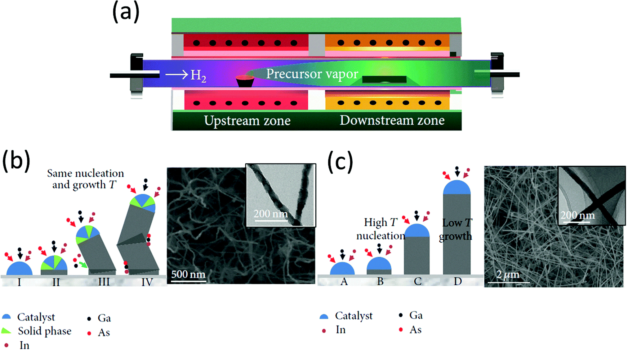 | ||
| Fig. 1 (a) Schematic representation of the typical SSCVD setup and the growth process. Not drawn in scale; (b) single-step growth method. Left: Schematic illustration of the growth mechanism of the single-step method, demonstrating a kinked morphology and surface coating during the NW growth; right: SEM and (inset) TEM images of the NWs grown using the single-step method; (c) two-step growth method. Left: Schematic illustration of the growth mechanism of the two-step method; right: SEM and (inset) TEM images of NWs grown using the two-step method. Reproduced from ref. 31 and 36 with permission from The American Chemical Society. | ||
Although the SSCVD growth method can be easily utilized to synthesize high quality and high density NWs such as InP and InAs (as shown in Fig. 2a and b) with metal (Au, Ni, or others) nanoclusters as catalysts,11,15,32–34 further technical modifications are still needed to apply the method to certain systems, especially for the synthesis of antimony (Sb)-based NW and arsenic (As)-based ternary NW materials, such as GaSb and InGaAs NWs. Because of the narrow direct bandgap and outstandingly high hole mobility, GaSb NWs have been extensively explored for various electronics and optoelectronics applications. However, the growth of high-quality III-Sb NWs is still challenging, because of the tendency of the constituent Sb to aggregate on top of the growing layer without being incorporated into the NW growth. Recently, we have demonstrated successfully a synthesis technique utilizing Au nanoclusters as the catalysts, and high density GaSb NWs on amorphous Si/SiO2 substrates via the surfactant-assisted SSCVD method are achieved.31,35 By adjusting the source temperature, the growth time, the carrier gas flow rate and optimizing sulfur surfactant loading, a Sb-supersaturated environment can be expected to be induced, which is favorable for the growth of high-quality GaSb NWs. Importantly, a sulfur surfactant is used to passivate the NW growing surface and this alleviates the uncontrolled radial growth. The obtained NWs, as shown in Fig. 2c, are crystalline and stoichiometric, with uniform diameters as well as minimal surface coatings. When configured into FETs, the NWs exhibit excellent p-channel device characteristics with a peak hole mobility of ∼200 cm2 V−1 s−1, this represents one of the best mobility values reported for any GaSb NW device to date.35
 | ||
| Fig. 2 Scanning-electron microscope images of InP (a), InAs (b), GaSb (c), and GaAs (d) nanowires grown using the VLS method. Reproduced from ref. 11, 32, 35 and 41 with permission from The Royal Society of Chemistry, The American Chemical Society, and The Nature Publishing Group. | ||
Moreover, it is difficult to obtain high-quality ternary InGaAs NWs with high growth yield using the standard SSCVD method. To overcome this, a simple but unique technique has been developed, and highly crystalline InGaAs NWs are synthesized by a two-step CVD growth method with high growth yield.36 The two step growth method, in which an additional nucleation step with a temperature higher than the growth temperature, is used before the regular growth step, and long, straight and defect free nanowires have been grown.36,37 For the conventional single-step growth, because the temperature difference between the catalytic eutectoid and the NW growth is small, the catalyst nanoparticles may not be homogeneous in the liquid or solid phase, resulting in an unevenly distributed growth rate which is the main reason for a kinked morphology (stage III), as shown in Fig. 1b. During the growth process, the precursor source atoms may impinge and diffuse onto the kinked surface due to heterogeneous catalytic favorable sites,36 which leads to a severe surface over-coating problem on the InGaAs NWs (stage IV). In contrast, the InGaAs NWs grown using a two-step method exhibit a much straighter as well as smoother surface with insignificant over-coating. During the higher temperature nucleation step, the catalyst is expected to be a homogenous liquid and hence no kinked structure will be nucleated. Hence, the nanowires will grow more uniformly without the kinked structures when they are grown at lower temperature, and the radial growth is limited so that no tapering and coating can be formed during the standard VLS growth process (stages C and D). The InGaAs NW FET, fabricated by the two-step-method grown nanowires, with reduced kinked morphology and surface coating along the nanowires, shows excellent electrical performances as reported by Hou et al.36,38,39
In addition, there have been two reports employing the two-step growth method to further reduce the defect density in GaAs nanowires.37,40 Joyce et al. used the two-step growth method to limit the radial growth and eliminate the twin defects at the same time.37 In another report, Han et al. eliminated the crystal defects of GaAs NWs by the same technique, and the as-grown NWs are shown in Fig. 2d.40,41 The transfer characteristics of the device, fabricated with GaAs nanowires synthesized using solid-source CVD, exhibit a switching from n-type conductivity to p-type conductivity when the diameter of the NWs decreases.41 This switching effect can be attributed to the acceptor-like states at the oxide interface depleting the conduction channel at the NW core. With thinner NWs, this effect dominates due to the larger surface-area-to-volume ratio, and the NW becomes p-type. For thicker NWs the donor-like crystal defects, such as As precipitates42–44 which are generated by insufficient Ga supersaturation on the catalytic tip during growth, neutralize the depletion of the oxide interface defects and, therefore, the NWs show intrinsic n-type conductivity. With this two-step growth, the multi-crystallinity and crystal defects can be significantly reduced due to improved crystallinity, and the NWs' conductivity can be manipulated by varying the NW diameters.
2.2. Core–shell configuration
Core–shell hetero-structures formed by the growth of crystalline overlayers surrounding the NW core can make use of the advantages of both materials, and offer enhanced electrical, optical, electrochemical, and mechanical properties,45–47 which are important for various applications. GaAs–AlGaAs NW is one of the most studied core–shell hetero-structures. GaAs NWs have higher mobility than silicon, making them potential candidates to replace silicon in next-generation electronic devices. Also, the direct band gap of GaAs makes it an ideal replacement for the indirect bandgap of silicon for optoelectronic applications, owing to its effectiveness in light absorption. However, GaAs NWs have relatively large density of surface defects, contributing to an accumulation layer that pins the surface Fermi energy and forms a depletion layer, which limits the performance of NW photoconductors; hence, the electron mobility is decreased substantially (usually lower than 1500 cm2 V−1 s−1).48 Also, the surface recombination velocity of GaAs is extremely high (106 cm s−1) and the carrier lifetime is extremely short (a few ps) as compared to other typical III–V materials.48 Hence, the motivation of developing GaAs/AlGaAs core–shell nanostructures is to passivate the GaAs core surface and to decrease the carrier traps by conformally coating it with a shell. With careful shell thickness adjustment, the electron mobility can be increased up to 3000 cm2 V−1 s−1, which is ∼65% of the mobility value of high-quality undoped bulk GaAs.49 The photoconductivity lifetime is also increased to the nanosecond range, reaching ∼1.6 ns. Furthermore, picosecond response time (less than 10 ps) has been achieved for GaAs/AlGaAs core/shell NW-based photodetectors with very low dark current and capacitance values, and their performance is considerably better than bare GaAs NW-based detectors, confirming the potential of core/shell NWs in high-speed imaging arrays and on-chip optical interconnects.50 Such a core–shell structure can be further developed into a core-multi-shell configuration and utilized as a single nanowire photodetector.Recently, Dai et al. demonstrated an efficient core–shell GaAs/AlGaAs NW photodetector operating at room temperature.51 The metal–semiconductor–metal (MSM) radial architecture NW photodetectors were fabricated by depositing selective Pt contacts on both the GaAs core and the AlGaAs shell as electrodes using a focus ion beam (FIB) system, and the corresponding SEM image of the photodetector structure is shown in Fig. 3a. The measured photoresponsivity of the single NW photodetector is shown in Fig. 3b, which shows a peak photo-responsivity of 0.57 A W−1 at λ = 855 nm.51 The simulated optical absorption maps across the cross-section of the nanowire (Fig. 3c) represent the spatial distributions of electromagnetic energy in the device, and three resonant modes corresponding to the optical modes in the GaAs core of the NW with AlGaAs shell confinement are indicated. The NW photodetector exhibits low dark current and high photo-responsivity, which can be attributed to the core–shell geometry. Combined with the Si delta (δ)-doping process, the core–shell NW-FET shows a superior low-temperature field-effect electron mobility of up to 5 × 103 cm2 V−1 s−1, a low subthreshold slope of 70 mV dec−1, and an excellent on/off ratio >104–105 at room temperature.52 Also, Jiang et al. reported the rational design and synthesis of InAs/InP core/shell NW hetero-structures with quantum-confined and high-mobility electron carriers. To be specific, the conduction band offset of InP (∼0.52 eV) can confine the electrons in the type-I quantum well structure. By capping the InAs surface with a 2–3 nm InP epitaxial shell, a high field-effect mobility of 11![[thin space (1/6-em)]](https://www.rsc.org/images/entities/char_2009.gif) 500 cm2 V−1 s−1 has been achieved at room temperature.53 With a 0.5–1 nm InP epitaxial shell, the low temperature (2 K) field-effect mobility increased by 2–5 times compared to bare InAs NW devices, and some even exceed 20000 cm2 V−1 s−1.54
500 cm2 V−1 s−1 has been achieved at room temperature.53 With a 0.5–1 nm InP epitaxial shell, the low temperature (2 K) field-effect mobility increased by 2–5 times compared to bare InAs NW devices, and some even exceed 20000 cm2 V−1 s−1.54
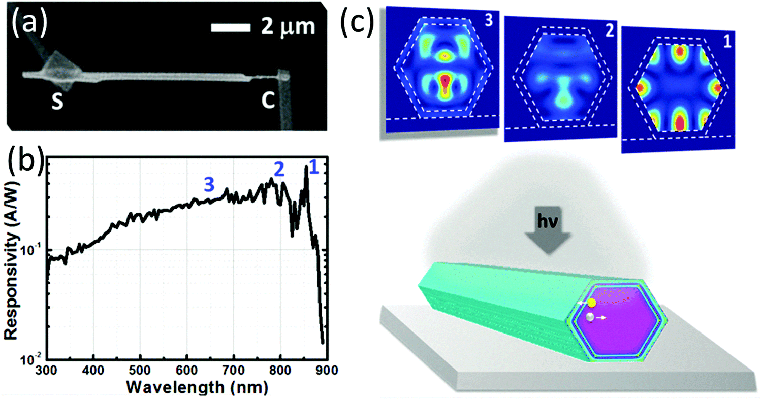 | ||
| Fig. 3 (a) SEM image of the MSM nanowire photodetector with selective contacts to the core C and to the shell S. The scale bar is 2 μm; (b) measured spectral photoresponsivity of the core–multishell nanowire photodetector under applied bias of VSC = 2 V; (c) simulated optical absorption maps across the section of the nanowire at wavelengths corresponding to peaks 1, 2, and 3, respectively. Reproduced from ref. 51 with permission from The American Chemical Society. | ||
2.3. Contact printing method
Since a single NW channel can only output a tiny current, usually less than 1 μA, and is subject to wire-to-wire variation, a contact printing technique can be utilized for the large-scale assembly of NW parallel arrays on both rigid and mechanically flexible substrates followed by subsequent device fabrication. This approach can provide high performance and stable device operation at low cost.13,14,16,55 A simple contact printing approach for the wafer scale assembly of highly ordered, dense and regular arrays of NWs with high uniformity and reproducibility was demonstrated by Fan et al.55 In this process, a growth substrate with dense NWs as the donor substrate was directionally slid on top of a receiver substrate coated with a lithographically patterned resist, resulting in the direct transfer of aligned NWs to the receiver chip, as shown in Fig. 4a. A lubricant can be used as a spacing layer between the two substrates and minimizes the NW–NW friction during the sliding process, and the density of the printed NWs can be easily modulated to meet the requirements of various NW-based device applications. After NW printing, the patterned resist was removed by a standard lift-off process, and the NWs were directly transferred from the growth substrate to the patterned regions of the substrate as parallel arrays. Fig. 4b and c present the optical and scanning electron microscopy (SEM) images of assembled Ge NWs on the receiver substrate, demonstrating that indeed the transferred NWs can form a uniform and well-aligned monolayer. Also, double layer printing of Si NW crosses can be achieved using a multi-step printing method as illustrated in Fig. 4d and f, and the controlled stacking of NW crosses indicates the versatility of the contact printing method for optoelectronic applications.55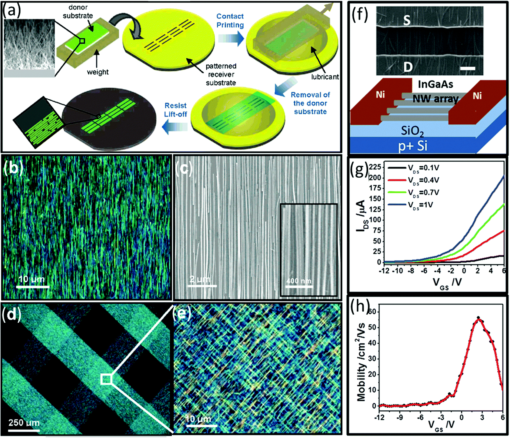 | ||
| Fig. 4 (a) Schematic of the process flow for contact printing of nanowire arrays; (b) dark-field optical and (c) SEM images of GeNWs (d ∼ 30 nm) printed on a Si/SiO2 substrate showing a highly dense and aligned monolayer of nanowires. The self-limiting process limits the transfer of NWs to a single layer, without significant NW bundling; (d and e) optical images of double layer printing for SiNW (d ∼ 30 nm) cross assembly; (f) (top) SEM and (bottom) schematic of a back-gated InGaAs NW array FET. The scale bar is 1 μm; (g) transfer characteristic of a representative InGaAs NW parallel device under VDS = 0.1, 0.4, 0.7, and 1 V, about 200 NWs bridging S/D; (h) mobility assessment of this NW array device under VDS = 0.1 V. Reproduced from ref. 36 and 55 with permission from The American Chemical Society. | ||
As expected, the contact printing process can also be widely adopted for III–V semiconductor nanowires, such as InAs, and InGaAs NWs.15,16,36 Hou et al. demonstrated the feasibility of large-scale integration of the NWs for electronic applications, and fabricated InGaAs NW parallel arrays using this contact printing method.36 The SEM image and schematic of the printed NW array FET device are shown in Fig. 4f, and the electrical transfer characteristics of a printed array with ∼200 nanowires in the channel are shown in Fig. 4g. The current density of this device is found to be ∼1 μA μm−1 at VDS = 1 V and VGS = 6 V with an ION/IOFF ratio of ∼500, and the corresponding field-effect mobility against gate voltage, VGS, is evaluated as shown in Fig. 4h. The NW device performance can be further improved by enhancement of the NW print density, the alignment, the channel length scaling, and the passivation of the NW surfaces. Besides, Javey et al. demonstrated, for the first time, the GHz device operation of InAs NWs arrays assembled on a mechanically flexible substrate.16 The NW arrayed transistors exhibit a maximum oscillation frequency of ∼1.8 GHz, and a cutoff frequency of ∼1 GHz, which is due to the high saturation velocity of electrons in the high-mobility InAs NWs, confirming the potential of NW array FET devices for future high-performance electronic device and sensor applications.
3. Optoelectronic properties of III–V nanowires
3.1. Light absorption
It is both experimentally and theoretically demonstrated that one-dimensional NWs can have better light absorption characteristics than their bulk counterparts.56–58 For nanostructured materials with dimensions comparable with or smaller than the wavelength of incident light, resonance will occur and ray optics is no longer valid. The light absorption area is enhanced, the physical cross-sectional projected area is greatly increased, and both photon absorption and photocarrier collection efficiencies are significantly improved.59–62 Simulation of light absorption of a horizontal nanowire lying flat down on a substrate has been carried out by Heiss and Morral, and their results are summarized in Fig. 5a–c.63 External quantum efficiency (EQE) refers to the efficiency calculated based on all the incident light (or photon), and internal quantum efficiency (IQE) designates the efficiency based on the already absorbed light. As a result of the built-in light concentration by Mie resonances, the absorption cross-section can be significantly larger than the physical cross-section of the nanowire. The simulated EQE/IQE ratio can be as high as 1, showing that the light absorption of NWs can be effective and comparable with their thin film counterparts. Furthermore, if the NWs are arranged in a two dimensional array in the wavelength scale, the total light absorption area can be 10 times as large as their projected area.64 This enhanced light absorption area enables vertical standing NW based photovoltaics having an efficiency of up to 40%.64 Even though resonance absorption is limited by the NW arrays, a large amount of material consumption is reduced due to the light concentration effect, and the efficiency can be improved further under a concentrated solar field.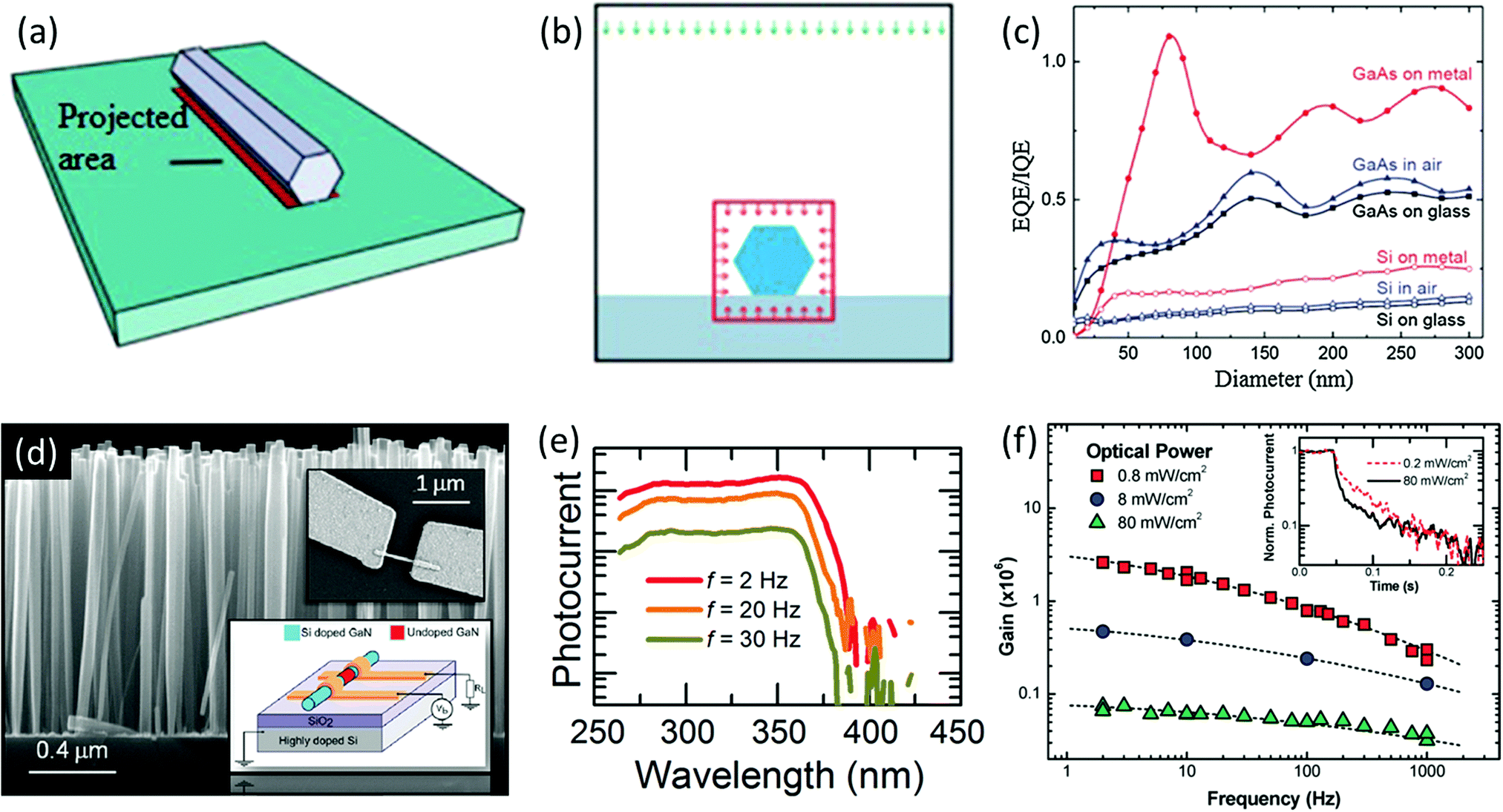 | ||
| Fig. 5 (a and b) Simulation results of light absorption of a horizontal nanowire on a substrate; (c) the EQE/IQE ratio of GaAs and Si NWs; (d) side-view SEM image of n–i–n GaN NWs on the Si(111) substrate. Insets: Top panel is the top-view SEM image of a contacted single NW; bottom panel shows the measurement scheme for characterization of a single NW device; (e) spectral response of a single NW under 3 V bias at a measurement frequency of 2, 20, and 30 Hz; (f) variation of the photodetector gain of a GaN NW under 3 V bias as a function of the measuring frequency for various excitation powers. Inset: Photocurrent decay from a single NW after UV (λ = 244 nm) illumination at 80 and 0.2 mW cm−2. The light was chopped at f = 2 Hz to minimize thermal effects. Reproduced from ref. 63 and 73 with permission from The AIP Publishing LLC and The American Chemical Society. | ||
Recently, efficient optical absorption of NW arrays has been extensively explored to achieve the optimized optical design of NW-based optoelectronic devices, such as photodetectors and photovoltaics.59,65–67 Although an apparent efficiency of 40% beyond the Shockley–Queisser limit has been accomplished by vertical-structured GaAs photovoltaics,64,68 the horizontal NW channel configured should possess higher light absorption characteristics than thin films even though the NW absorption thickness is lower, confirming the low-cost advantages of NW based photovoltaics as well as photodetectors by the resonant light absorption effect. Han et al. reported high-density GaAs NWs with a superior apparent sunlight-to-electricity conversion efficiency of up to ∼16% in a moderate Schottky barrier structured photovoltaic cell; the result can be attributed to the efficient light absorption and enhanced electron/hole diffusion length due to the excellent crystal quality obtained by the two-step growth process.56 The photovoltaic output can be further enhanced by connecting individual cells in series and in parallel, as well as by fabricating NW array solar cells via contact printing showing an overall efficiency of 1.6%, demonstrating the promising perspective of flexible and transparent III–V NW-based photodetectors and photovoltaics.
3.2. Photoconductive gain
For high-speed optical data communication applications, the device must have high response to photo-excitation and relax to the dark state immediately after the light source is switched off.69 In the application to photodetectors and photovoltaics, the sensitivity to light (i.e. photoconductivity) is one of the most important performance parameters. Semiconductor NWs can yield higher light sensitivity than their bulk counterparts and they contain an extremely high density of surface states due to their large surface-to-volume ratios and small dimensions. It is found that the photo-generated excess carriers do not recombine immediately after the light source is turned off, thus the excess photocurrent decays slowly, reaching the dark current level in tens of seconds and is called persistent photoconductivity (PPC).20 As the NW geometry dictates the surface potential, the Fermi energy pinning as well as determines the corresponding carrier distribution, the NW dimensions would then have a substantial influence on the dark- and photo-currents in the NWs. For example, III–V semiconductor NWs exhibit extremely high photoconductive gain because of the prolonged photocarrier lifetime which significantly reduces the carrier transit time, and can be attributed to the high mobility achievable in high-quality and defect-free single crystalline NWs combined with the small inter-electrode distances.70,71 In brief, the photoconductive gain is defined as the ratio between the number of electrons collected per unit time and the number of absorbed photons per unit time (G = Nelectron/Nphoton). In any case, the large photoconductive gain is achieved at the expense of dynamic response. Optimization of the electrode geometry can minimize the carrier transit time and both high sensitivity and large gain-bandwidth products can be achieved simultaneously.An ultrahigh photocurrent gain of 5.0 × 10⁴–1.9 × 10⁵ was reported in GaN NW UV photodetectors, the gain is ∼3 orders of magnitude higher than that of thin film counterparts, which is due to the strong surface electric field of NWs instead of the trap-dominant high-gain mechanism in a one-dimensional nanostructure.72 González-Posada et al. reported a unique photocurrent phenomenon observed in single n–i–n GaN NWs as shown in Fig. 5d; the device has a high photoconductive gain in the range of 105–108, an ultraviolet (350 nm) to visible (450 nm) responsivity ratio larger than 6 orders of magnitude, and is independent of the measured frequency.73 The NW photo-response was investigated by spectrally resolved measurements and is shown in Fig. 5e. The result shows a flat spectral response for wavelength above the GaN bandgap (λ < 350 nm), and the response for wavelength beyond 450 nm is below the resolution limit of the system. It can be seen that the responsivity ratio of UV (350 nm)/visible (488 nm) is more than 6 orders of magnitude. Variation of the photodetector gain was also measured as a function of chopping frequency in order to investigate the photo-response dynamics, as shown in Fig. 5f. A large bandwidth for high excitation power is related to a decrease in the photodetector gain. A high photoconductive gain of up to 20000 at low laser excitation is also achieved in a single GaAs NW photodetector, demonstrating the band-edge absorption profile of single GaAs NWs and the existence of leaky-mode resonance.74
4. III–V nanowire photodetectors
4.1. UV photodetectors
UV photodetectors (UV PDs) are of great interest and have various commercial, military, and biological applications. UV photodetectors based on single GaN NWs, with a wide and direct bandgap, exhibit rectifying behavior and relatively fast photo-response, and are regarded as promising visible-blind PDs. W. Y. Weng et al. investigated the transient response of the GaN NW photodetector by switching the UV excitation on and off cyclically, and the response of the photodetector is stable and reproducible with the on/off current contrast ratio of about 1000.75 As the UV excitation is turned on, the photocurrent increases rapidly at the beginning and then the increase slows down, this is due to the hindered speeds of the charge-carrier collection by the surface defect related trapping centers under UV excitation. Similar slow response can also be observed as the UV light is turned off, this is due to charge–carrier recombination.76 Compared with the conventional 2-D GaN PD, the GaN NW PD can achieve the larger UV-to-visible rejection ratio and an ∼1000 times larger photocurrent, confirming the superiority of the III–V NW UV photodetectors.Recently, Liu et al. fabricated a GaN NW-based photodetector with Ag NWs as transparent electrodes.77 From the I–V characteristics of the photodetector in the dark and under the illumination of a xenon lamp, it can be seen that the ratio of photocurrent to dark current of the photodetector is ∼140 operated in ambient air, this value is higher than the reported ratios of illumination to dark current. Under UV excitation, the electrons will transit from GaN to Ag, establishing a uniform Fermi level as the work function of Ag is higher than that of GaN, and the photo-generated carrier will contribute to the photocurrent, resulting in a low Schottky barrier and, at reverse bias, causes an increase in current compared to that at forward bias. With the periodic turning on and off of the xenon lamp in air or in a vacuum, the photodetector exhibits a fast photocurrent response to the xenon light exposures with approximately rectangular shaped curves, indicating a stable and reproducible response to the UV light. The high crystal quality of GaN NWs and the Schottky contact of GaN NWs with Ag NWs lead to a large photoconductive gain, and the ratio of photocurrent to dark current of the photodetector in a vacuum is about 1400. The photodetector shows a fast and high responsivity at 350 nm; however, due to absorption of Ag NWs, it shows less sensitivity to UV around 300 nm. GaN NW UV photodetectors with graphene transparent contact have also been fabricated in order to achieve better UV transparency, and the detector exhibits a responsivity of 25 A W−1 at 1 V bias at 357 nm wavelength with low excitation power.78
Further improvement has been made by fabricating single-NW UV photodetectors relying on the carrier generation in GaN/AlN quantum disks (QDiscs).79 Two heterostructured NW samples with different QDiscs thicknesses are analyzed and the STEM images are shown in Fig. 6a. Room temperature photoluminescence spectra of the NWs are shown in Fig. 6b and a low-energy peak attributed to QDisc emission is observed in GaN/AlN heterostructures in NWs. The dark I–V characteristics of single NWs are compared to the I–V characteristics under UV illumination at λ = 300 nm with a power density of 5 mW cm−2 as shown in Fig. 6c, and the device has a high responsivity of 2 × 10³ A W−1 at λ = 300 nm and a high ratio of photocurrent to dark current of the photodetector of up to 5 × 10² for sample 2, the improved results are mainly attributed to the insertion of an axial heterostructure which drastically reduces the dark current with respect to binary NWs.
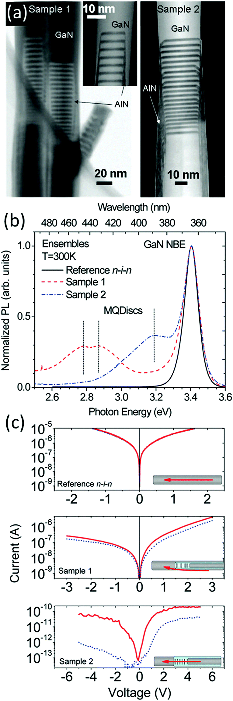 | ||
| Fig. 6 (a) (left) STEM image of nanowires from sample 1. Inset displays a high-angle annular dark field (HAADF) STEM image showing details of the external GaN shell; (right) HAADF STEM image of a nanowire from sample 2; (b) room-temperature PL spectra of the nanowire ensembles of the reference n–i–n sample (black solid line), of sample 1 (red dashed line) and of sample 2 (blue dash-dotted line); (c) the I–V characteristics at T = 300 K of the nanowire from the reference sample, sample 1, and sample 2. The blue dotted lines correspond to the dark current; the red solid lines correspond to illumination under continuous 300 nm light with 5 mW cm−2 power density. The sketches on the lower right-hand side of each plot depict the conduction regime for each sample. Reproduced from ref. 79 with permission from The American Chemical Society. | ||
4.2. Visible-to-near-IR photodetectors
Among all the III–V semiconductor NWs, InAs NWs are regarded as a promising material for broad-spectrum detection applications, ranging from visible to infrared regions due to their high carrier mobility, narrow band gaps for infrared detection, and surface Fermi level pinning above the conduction band edge.80,81 They can be used for ultra-high frequency electronics owing to the radio frequency response of InAs NW array FETs,16 or adopted as potential candidates for ballistic transistors due to their long bulk electron mean free path.82 However, for the NW-based photodetectors numerous minority carriers recombine before being collected and contribute to the photocurrent, resulting in a short minority carrier lifetime and is a common problem that needs to be resolved. Recently, InAs NW phototransistors based on the majority-carrier-dominated photodetection mechanism were investigated by Guo et al.83 A back-gated core/shell-like InAs NW transistor was fabricated as shown in Fig. 7a, and InAs NWs were synthesized using the CVD method with a self-assembled “photogating layer” (PGL) formed near the NW surface. This PGL can trap electrons generated from the NW core under light illumination and form a built-in electric field to modulate the core conductance. Before light illumination, the free electrons in the NW core flow under the action of the electric field to form the dark current, then the electrons are excited into the PGL under light excitation as shown in Fig. 7b. In the PGL, there are many distributed trapping centers and photo-excited electrons are captured and recombine to form dark current in the core immediately (Fig. 7c). The anomalous switching between the low current state under green laser illumination and the high current state under dark conditions exhibits highly stable and reproducible characteristics, and a high photoconductive gain of ∼−105 and a fast response time of 12 ms are obtained at room temperature (Fig. 7d and e), demonstrating that the III–V NW-based photodetectors are promising for novel, high-sensitivity, broad-spectrum and room-temperature detection.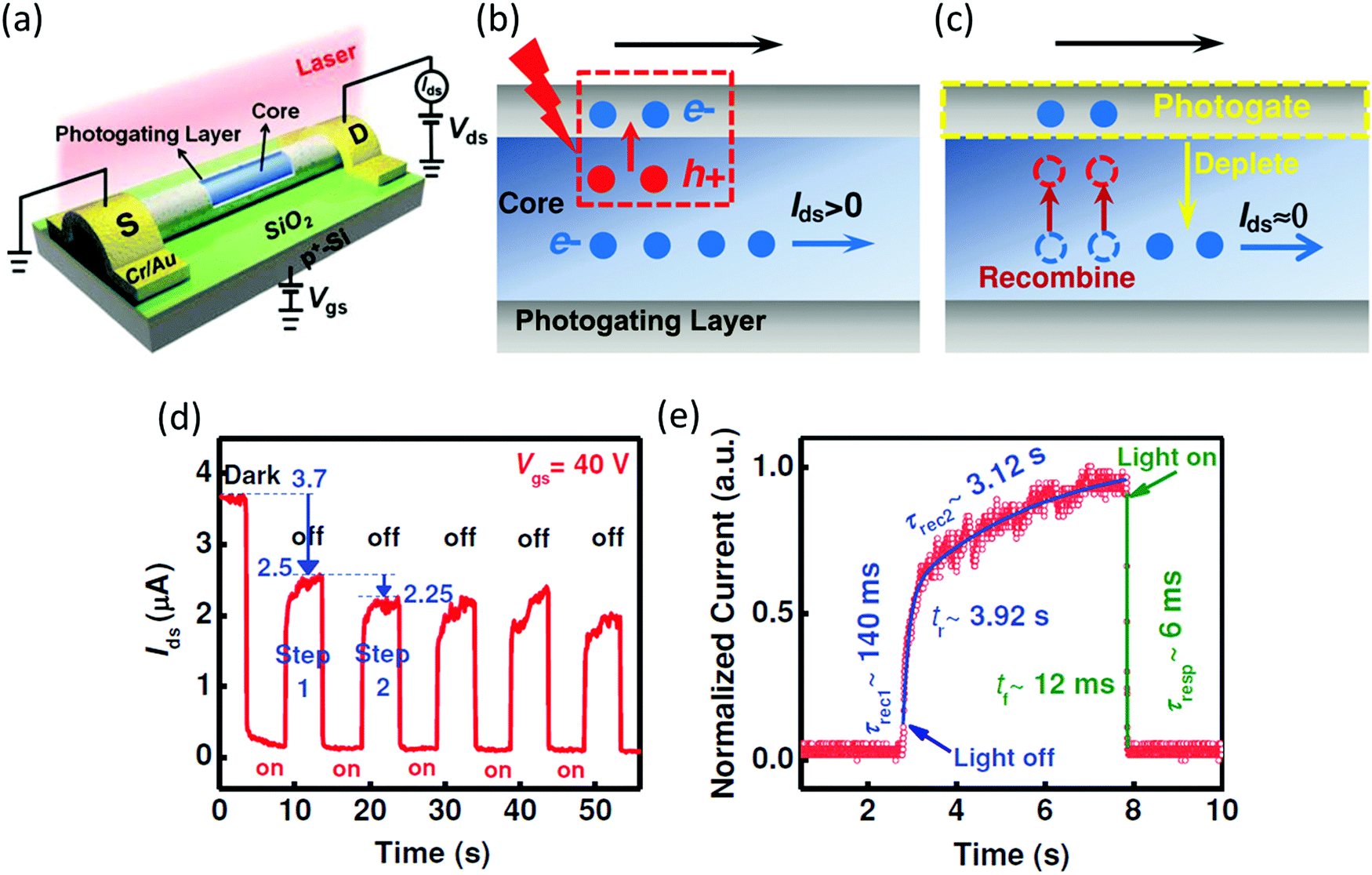 | ||
| Fig. 7 (a) A schematic illustration of the InAs NW transistor; (b) the process of photogenerated electron–hole pairs. Under light illumination, electrons (e−) are excited into the PGL and remain trapped. Holes (h+) are left in the NW core; (c) the process of majority carrier dominated photodetection. Holes recombine with free electrons in the core. Electrons trapped in the PGL induce a photogating effect on the core; (d) photoresponse properties of the InAs NW transistor under green laser illumination (532 nm, 8 mW mm−2) at Vds = 1 V in air, acquired for the gate voltage of 40 V. The photoconductance modulation is induced by manipulating a shutter for the light on/off at an interval of 5 s; (e) a single normalized modulation cycle measured with a light intensity of 8 mW mm−2 (open circles) at Vgs = 0 V and Vds = 1 V. The blue and green lines fit to the rising (recovery τrec1 and τrec2) and falling (response τresp) edges, respectively. Reproduced from ref. 83 with permission from The John Wiley and Sons. | ||
The first room-temperature operated InAs NW infrared photodetectors having a detection wavelength up to ∼1.5 μm have been reported by J. Miao et al.84 The optoelectronic properties of the InAs NWs, especially the effects of surface defect states and atmospheric molecules on its photoresponse in the infrared region, were investigated in detail. From the photocurrent spectra of a representative InAs NW near-infrared photodetector with wavelength changing from red (λ ∼ 632 nm) to near-infrared light (λ ∼ 1.5 μm), the photodetector shows a distinct photo-response to different wavelengths, as shown in Fig. 8a. The output characteristics of the photocurrent and the switching behavior were carried out at room temperature, and the photo-responsivity of Schottky–Ohmic contacted photodetectors is found to be ∼5.3 × 10³ A W−1, this value is ∼300% larger than that of Ohmic–Ohmic contacted devices (∼1.9 × 10³ A W−1) due to the strong built-in electric field at the InAs NW/Au electrode Schottky junction. Fig. 8b shows that the on–off photo-switching behavior remains stable after 14 cycles, indicating that the Schottky–Ohmic contacted InAs NW photodetectors have good stability. It is found that atmospheric molecules can reduce the current density, due to the charge transfer and the electrostatic interaction between InAs NWs and atmospheric molecules, and the metal-cluster decoration can increase the corresponding photo-responsivity by ∼3 times.
 | ||
| Fig. 8 (a) Photocurrent spectra of InAs NW near-infrared photodetectors changing from red to near-infrared light. The inset is the SEM image of a representative InAs NW photodetector. The scale bar is 1 μm; (b) time-dependent photoresponse of the Schottky–Ohmic contacted InAs NW photodetectors; (c) I–V curves for a representative In0.65Ga0.35As nanowire photodetector under light illumination with different wavelengths (Pin = 15.8 mW cm−2) at room temperature. Inset: The SEM image of a fabricate photodetector, the scale bar is 2 μm; (d) time dependent photocurrent response to 1600 nm light under 0.5 V bias. Reproduced from ref. 84 and 85 with permission from The American Chemical Society and The Springer. | ||
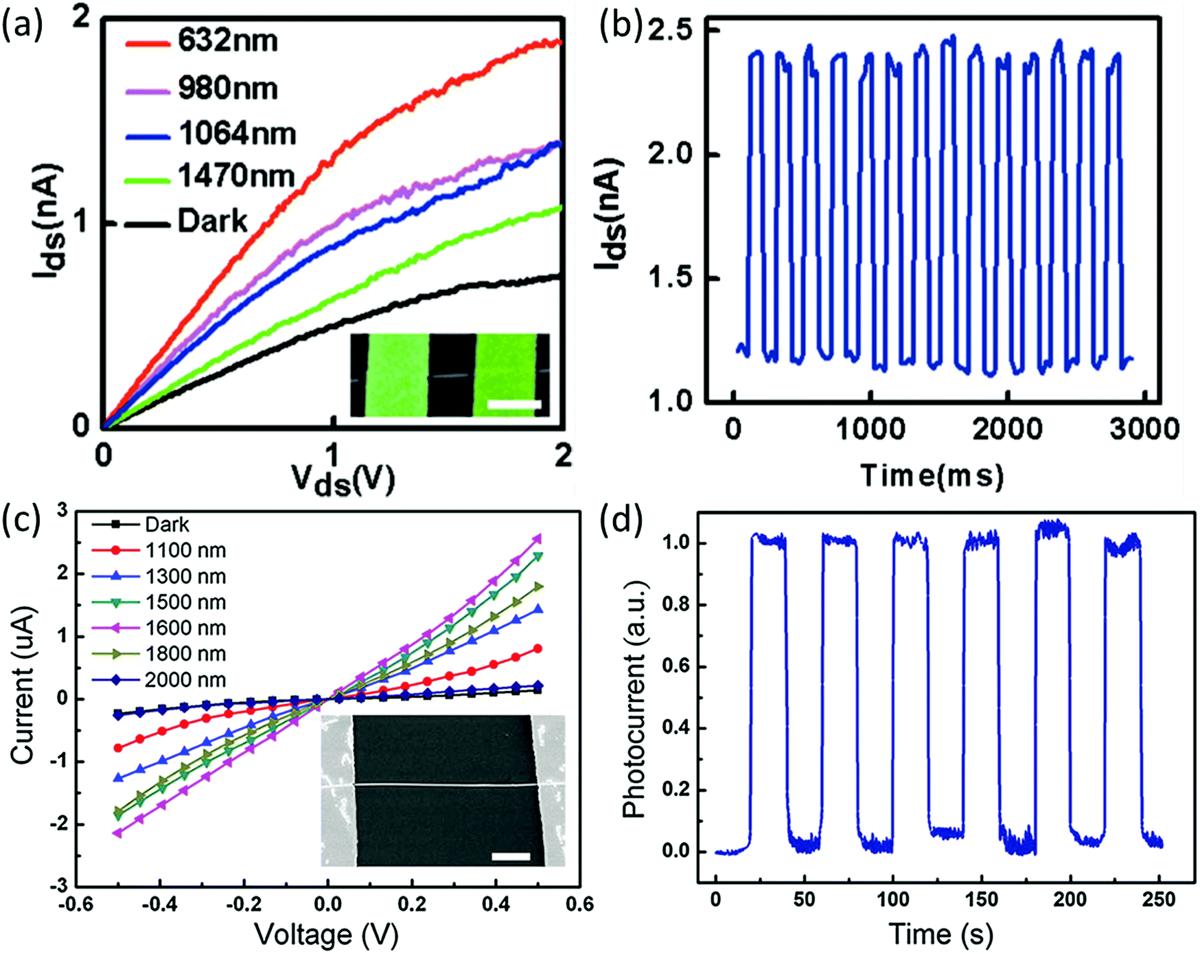
Recently, high-performance InGaAs NW near-infrared photodetectors have been reported, with good photo-response over a broad wavelength range from 1100 to 2000 nm.85Fig. 8c shows the I–V curves of a representative InGaAs NW photodetector measured under the illumination of a beam of monochromatic light ranging from 1100 to 2000 nm wavelength at room temperature, and the device exhibits good photo-response ability in the near-infrared wavelength region. The response time and the recovery time are calculated to be 70 and 280 ms from the time-related response of the photocurrent to illumination light at 1600 nm, as shown in Fig. 8d, and these values are comparable to those of InAs NW photodetectors.83 Graphene/InAs NW heterojunction near-infrared photodetectors have been reported with a large photo-responsivity of 0.5 A W−1 and a distinct Ilight/Idark ratio of 5 × 10² in the infrared region (λ = 1 μm), and these values are much larger than those of graphene infrared photodetectors.86 Other III–V semiconductor NWs, such as GaAsSb NWs, have also been reported as room-temperature near-infrared photodetectors. The devices exhibit a wide spectrum response in the near-infrared region and have the highest response peak located in the optical communication band,87,88 indicating that III–V NWs have potential applications as integrated optoelectronic devices for visible and near-infrared radiation imaging, sensing, information communications and processing.
4.3. IR photodetectors
Photodetectors operating in the mid- to long-wavelength infrared band (3–14 μm) are important for thermal imaging, gas analysis, and remote pollution monitoring at room temperature. Compared with other III–V NWs, InAsSb NWs are a suitable material due to their tunable bandgap, high mobility and thermal conductivity. InAs/InAsSb NW infrared photodetectors with varying Sb compositions have been fabricated and investigated by Svensson et al.89 A representative I–V characteristic of the InAs/InAs1−xSbx NW channel with x = 0.76 in the dark and with all-wavelength IR illumination is shown in Fig. 9a. The illumination results in a photocurrent of a few 10 s of nA per NW with a bias voltage of 0.25 V, and the composition has a minimal effect on the spectral response. The spectrally resolved photocurrents, however, are strongly diameter dependent, and the diameter of the NWs can be adjusted to obtain peak absorption close to the InAsSb band gap, enabling the achievement of more than 1 order of magnitude higher absorption as compared to that of a thin film structure. The experimental data are in good agreement with numerical simulations, indicating that the peaks are due to the resonant modes that enhance the coupling of light to the NWs, as shown in Fig. 9b. A maximum 20% cutoff wavelength of 5.7 μm has been obtained, and photodetection of InAsSb NW arrays integrated on Si substrates has also been demonstrated, confirming that InAsSb NWs are suitable for infrared photodetectors due to their narrow band gap, high crystallinity and highly efficient absorption at a specific wavelength.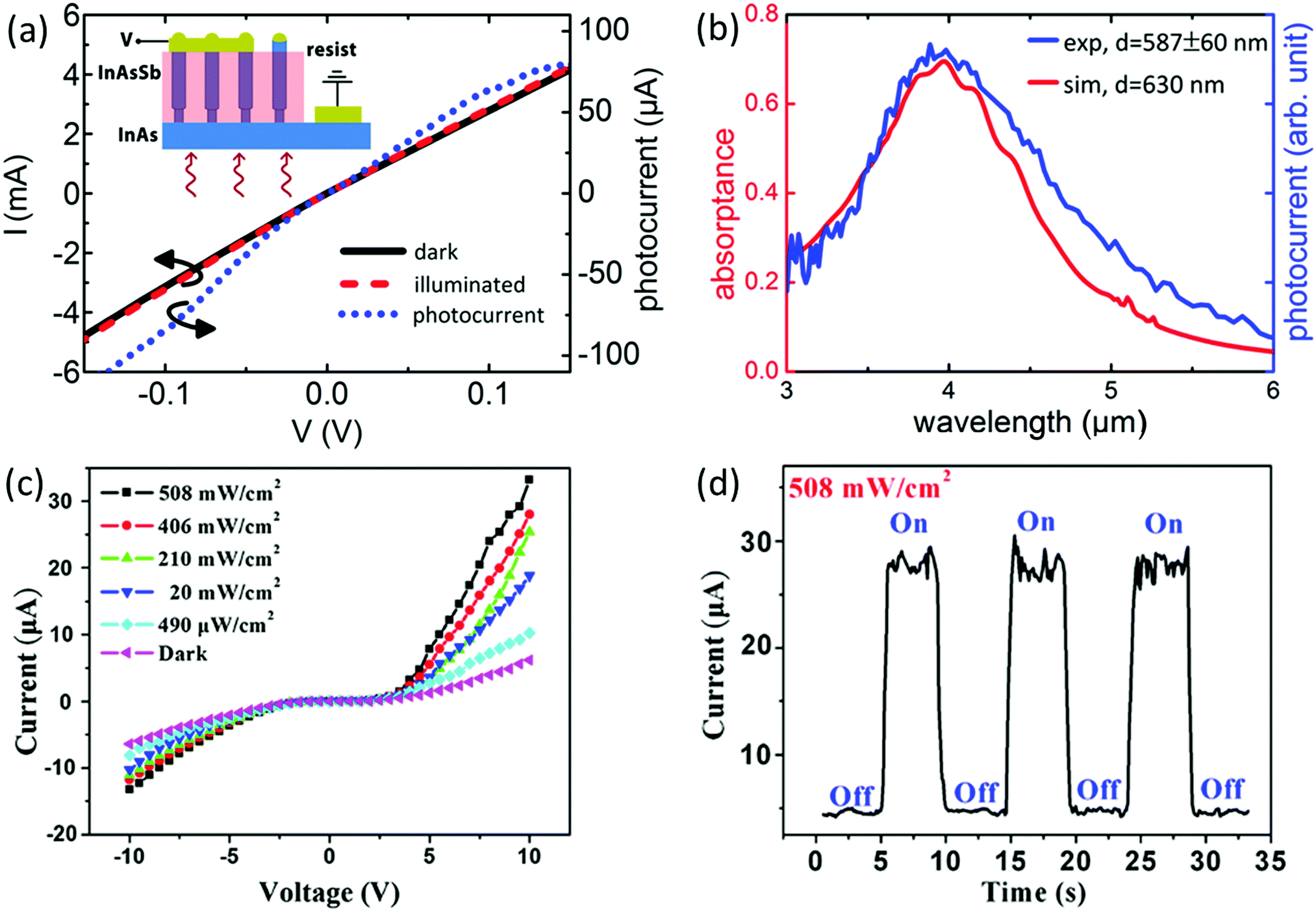 | ||
| Fig. 9 (a) Current–voltage characteristics at 5 K for a device with ∼8000 InAs/InAs1−xSbx wires with x = 0.76, d = 587 ± 60 nm, and a length of 1.95 μm in the dark and with all-wavelength illumination from a global source. Inset depicts a back-side illuminated nanowire array photodetector; (b) photocurrent spectra of InAs/InAs1−xSbx nanowires with composition x = 0.77 ± 1 nm and simulated absorptance for arrays of 6 μm long InSb wires at a constant d/p = 0.2; (c) I–V curve of an InSb nanowire under irradiation of light with different intensities; (d) the photocurrent behaviors of the InSb nanowire illuminated under a light intensity of 508 mW cm−2 as switch on and off states. Reproduced from ref. 89 and 90 with permission from The American Chemical Society and The Springer. | ||
Among typical III–V materials, InSb NWs have the smallest band gap and high carrier mobility, thus, they are considered as useful materials for mid- to long-wavelength IR photodetectors.90,91 Kuo et al. reported a high sensitivity middle-wavelength infrared photodetector based on a single InSb nanowire, and the device exhibited excellent stability, good photoconductive performance, reproducibility, superior responsivity (8.4 × 10⁴ A W−1), and quantum efficiency (1.96 × 10⁶%) detecting mid-infrared light at 5.5 μm wavelength.90Fig. 9c shows the I–V curves of InSb NW under irradiation of light with a wavelength of 5.5 μm and different light intensities. The photocurrent increases with increasing light intensity, and is consistent with the carrier generation efficiency being proportional to the absorbed photon flux. The time-dependent photo-response of the InSb NW was also measured using periodically on and off light, as shown in Fig. 9d. The response exhibits a good, clear, and stable variation, and simulation results also confirmed that InSb NWs are promising candidates for high-sensitivity IR photodetectors.91
5. III–V nanowire solar cells for flexible and transparent photovoltaics application
Excellent photon-to-electricity conversion efficiency, extraordinary radiation hardness, good optical transparency and inherent mechanical flexibility of III–V semiconductor NWs make them promising candidates for smart systems such as transparent and flexible photovoltaics.92–95 The development of large-scale integration of single crystalline NW arrays on flexible and transparent substrates has enabled the configuration and integration of solar cells for next-generation smart solar energy harvesting devices. Recently, facile Schottky barrier structured GaAs NW solar cells employing enhanced Au–Al asymmetric contacts were fabricated with the highest single NW photovoltaic apparent efficiency of up to 16% under air mass (AM) 1.5 global illumination.96 To achieve low-temperature solar cell fabrication, the Schottky barrier photovoltaic structure, instead of high-temperature p–n junction formation, was implemented by simply using asymmetric metal electrodes with one electrode (e.g. Au) having a relatively higher work function (W) while the other (e.g. Al) has lower W, as illustrated in Fig. 10a. The Au electrode with higher W would constitute a Schottky contact to photoelectrons of the GaAs NW, while the Al electrode with lower W would yield a Schottky contact to the photogenerated holes. From the I–V characteristics of one representative NW solar cell in Fig. 10b, a high apparent energy conversion efficiency of 16% was achieved based on a simple horizontal Schottky photovoltaic structure, which is even higher than those of the complicated p–i–n NW structures.97,98 Although the obtained efficiency is high, the single NW solar cells have relatively low output voltage and current. For the purpose of their practical applications, the GaAs NW parallel arrays were also fabricated using the contact printing method as mentioned before. As compared to that of the single NW device, the output performance of this NW array cell was significantly improved as shown in Fig. 10c, with the estimated conversion efficiency of ∼11% by considering the total absorption area of the NWs under AM 1.5 G illumination. The GaAs NW array Schottky solar cell shows respectable and uniform photovoltaic performance, with higher efficiency achievable by fabricating higher density NW arrays with optimized NW contact printing.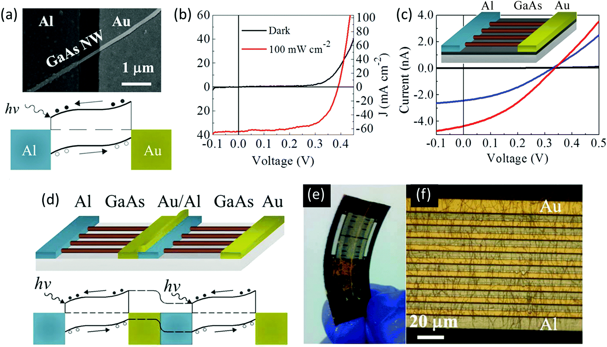 | ||
| Fig. 10 (a) SEM image and the corresponding band diagram of the single GaAs NW Schottky barrier solar cell with Au–Al electrodes; (b) I–V curves of the solar cell in (a); (c) I–V curves of the GaAs NW array solar cell fabricated by contact printing with optimized Au–Al asymmetric Schottky electrodes. Inset depicts device schematic of the GaAs NW array Schottky solar cell; (d) device schematic and corresponding band diagram of the transparent or flexible GaAs NW array Schottky solar cells; (e) photograph and (f) microscope image of the flexible GaAs NW array Schottky solar cells fabricated on polyimide. Reproduced from ref. 96 with permission from The American Chemical Society. | ||
The development of transparent and mechanically flexible solar cells is an essential step in the effort to develop a next-generation smart photovoltaic system. In this work, GaAs NW array Schottky solar cells were also built on nonconventional substrates for smart photovoltaics such as fabricating on glass for transparent solar cells as well as on polyimide for flexible photovoltaic cells. Fig. 10d depicts the device schematic and band alignment of the GaAs NW array Schottky solar cell connected in tandem readily by conventional lithography. For the transparent solar cell, the output voltage is scaled linearly with the number of cells connected in series, indicating the uniformity of NWs printed in the device channel suitable for large-scale applications. Also, the optical transparency of these cells fabricated on glass is also assessed and confirmed, suggesting the potential usage of these Schottky cells for smart windows. Fig. 10e and f present the picture and microscope image of flexible GaAs NW array Schottky solar cells fabricated onto the polyimide substrate. The output performance was slightly lower than the ones fabricated on glass due to inefficient NW printing on a nonsmooth surface. Although the efficiency of these proof-of-concept smart solar cell examples is relatively lower than that of single NW devices, the contact resistance will be optimized further and the NW density can be further enhanced by improved contact printing or other NW alignment techniques to obtain higher output current. These transparent and flexible Schottky solar cells, based on high performance GaAs NWs synthesized cost-effectively on noncrystalline substrates, are demonstrated with great promise for next-generation smart solar energy harvesting devices.
6. Conclusions and future work
In summary, III–V semiconductor NW-based photodetectors are promising candidates for high-sensitivity broad-spectrum room-temperature detection, and show potential applications as integrated optoelectronic devices for photovoltaics, radiation imaging, sensing, information communications and processing. In this paper, recent progress made in the area of III–V NW-based photodetectors has been reviewed, from the synthesis and assembly of III–V NWs, the precise manipulation of optoelectronic properties, and all the way to photodetector applications. Due to the setup simplicity and good controllability, the solid-source CVD growth method has been widely employed for the growth of various III–V NW materials. In general, by properly controlling the experimental parameters, such as the source composition, the catalyst, the growth temperature, the time duration and gas flow, and so forth, NWs with desirable chemical composition, morphology and tailorable properties could be synthesized, thus providing broad opportunities in the exploitation of different potential applications of NWs. Understanding the optoelectronic properties of NW materials is of great importance for the optimization of NW-based photodetectors. Light absorption and photoconductive gain have been investigated in III–V semiconductor NWs, and the results show that III–V NWs exhibit effective light absorption and high photoconductive gain, confirming the potential of the materials as active components for photodetectors. By developing core–shell hetero-structures, the surface of III–V NWs can be passivated, and the electron mobility and the photoconductivity lifetime can be increased further, resulting in high photo-responsivity in core–shell configured NW photodetectors.Many advanced research studies on III–V NW-based photodetectors operating in the UV, visible or infrared spectra range has been reported, and some representative investigations were discussed in this paper. For UV photodetectors, GaN NWs with a wide and direct bandgap exhibiting rectifying behavior and a relatively fast UV photo-response have been demonstrated as a promising candidate active material. Further improvement can be made by introducing hetero-structure geometries in order to reduce the dark current. Moreover, InAs NWs are considered as promising materials for broad-spectrum detection applications covering the visible to infrared regions, and the photo-response and photoconductive gain of the photodetectors can be enhanced by forming a PGL or metal-cluster decoration. InSb NWs and InAsSb NWs are also suitable materials for infrared detection because of their narrow band gap and high mobility. Future works can be focused on the reduction in the leakage current density in order to achieve high-performance and low noise III–V NW-based photodetectors.99
In order to develop an all-printable technology for inorganic electronics and sensors that deliver high performances and stable device operations at low cost, the contact printing method is utilized for the direct transfer and assembly of parallel-array NWs on various types of substrates. High-performance III–V NW solar cells can be easily integrated on the glass and plastic substrates for transparent and flexible photovoltaics, which explicitly demonstrates the outstanding versatility and promising perspective of these NW Schottky photovoltaics for next-generation smart solar energy harvesting devices. Further studies are still required to tackle the leakage current and surface-trap state issues of the NWs, and the sensitivity and precision of the NW-based large-scale integration of photodetector and photovoltaic arrays need to be improved for practical applications.
Acknowledgements
This work was supported by the General Research Fund of the Research Grants Council of Hong Kong SAR, China (Grant No. CityU 11213115), the National Natural Science Foundation of China (Grant No. 51672229), and the Science Technology and Innovation Committee of Shenzhen Municipality (Grant No. JCYJ20160229165240684).References
- X. Duan, C. Niu, V. Sahi, J. Chen, J. W. Parce, S. Empedocles and J. L. Goldman, Nature, 2003, 425, 274–278 CrossRef CAS PubMed.
- X. Duan, Y. Huang, Y. Cui, J. Wang and C. M. Lieber, Nature, 2001, 409, 66–69 CrossRef CAS PubMed.
- N. Han, F. Wang, J. J. Hou, S. P. Yip, H. Lin, F. Xiu, M. Fang, Z. Yang, X. Shi, G. Dong, T. F. Hung and J. C. Ho, Adv. Mater., 2013, 25, 4445–4451 CrossRef CAS PubMed.
- M. Law, L. E. Greene, J. C. Johnson, R. Saykally and P. Yang, Nat. Mater., 2005, 4, 455–459 CrossRef CAS PubMed.
- P. K. Mohseni, A. Behnam, J. D. Wood, X. Zhao, K. J. Yu, N. C. Wang, A. Rockett, J. A. Rogers, J. W. Lyding and E. Pop, Adv. Mater., 2014, 26, 3755–3760 CrossRef CAS PubMed.
- A. V. Thathachary, N. Agrawal, L. Liu and S. Datta, Nano Lett., 2014, 14, 626–633 CrossRef CAS PubMed.
- J. Wallentin, N. Anttu, D. Asoli, M. Huffman, I. Åberg, M. H. Magnusson, G. Siefer, P. Fuss-Kailuweit, F. Dimroth and B. Witzigmann, Science, 2013, 339, 1057–1060 CrossRef CAS PubMed.
- H. W. Shin, S. J. Lee, D. G. Kim, M.-H. Bae, J. Heo, K. J. Choi, W. J. Choi, J.-w. Choe and J. C. Shin, Sci. Rep., 2015, 5, 10764 CrossRef CAS PubMed.
- K. Tomioka, M. Yoshimura and T. Fukui, Nature, 2012, 488, 189–192 CrossRef CAS PubMed.
- T. P. Bartel, P. Specht, J. C. Ho and C. Kisielowski, Philos. Mag., 2007, 87, 1983–1998 CrossRef CAS.
- A. C. Ford, J. C. Ho, Y.-L. Chueh, Y.-C. Tseng, Z. Fan, J. Guo, J. Bokor and A. Javey, Nano Lett., 2008, 9, 360–365 CrossRef PubMed.
- A. C. Ford, S. Chuang, J. C. Ho, Y. L. Chueh, Z. Fan and A. Javey, Nano Lett., 2010, 10, 509–513 CrossRef CAS PubMed.
- Z. Fan, J. C. Ho, T. Takahashi, R. Yerushalmi, K. Takei, A. C. Ford, Y. L. Chueh and A. Javey, Adv. Mater., 2009, 21, 3730–3743 CrossRef CAS.
- T. Takahashi, K. Takei, J. C. Ho, Y.-L. Chueh, Z. Fan and A. Javey, J. Am. Chem. Soc., 2009, 131, 2102–2103 CrossRef CAS PubMed.
- A. C. Ford, J. C. Ho, Z. Fan, O. Ergen, V. Altoe, S. Aloni, H. Razavi and A. Javey, Nano Res., 2008, 1, 32–39 CrossRef CAS.
- T. Takahashi, K. Takei, E. Adabi, Z. Fan, A. M. Niknejad and A. Javey, ACS Nano, 2010, 4, 5855–5860 CrossRef CAS PubMed.
- Y.-Z. Long, M. Yu, B. Sun, C.-Z. Gu and Z. Fan, Chem. Soc. Rev., 2012, 41, 4560–4580 RSC.
- C. H. Lee, D. R. Kim and X. Zheng, Nano Lett., 2011, 11, 3435–3439 CrossRef CAS PubMed.
- S. Ju, A. Facchetti, Y. Xuan, J. Liu, F. Ishikawa, P. Ye, C. Zhou, T. J. Marks and D. B. Janes, Nat. Nanotechnol., 2007, 2, 378–384 CrossRef CAS PubMed.
- C. Soci, A. Zhang, X.-Y. Bao, H. Kim, Y. Lo and D. Wang, J. Nanosci. Nanotechnol., 2010, 10, 1430–1449 CrossRef CAS PubMed.
- R. Yan, D. Gargas and P. Yang, Nat. Photonics, 2009, 3, 569–576 CrossRef CAS.
- W. Lu and C. M. Lieber, J. Phys. D: Appl. Phys., 2006, 39, R387 CrossRef CAS.
- K. A. Dick, K. Deppert, T. Mårtensson, B. Mandl, L. Samuelson and W. Seifert, Nano Lett., 2005, 5, 761–764 CrossRef CAS PubMed.
- H.-J. Choi, Semiconductor Nanostructures for Optoelectronic Devices, Springer, 2012, pp. 1–36 Search PubMed.
- A. I. Persson, M. W. Larsson, S. Stenström, B. J. Ohlsson, L. Samuelson and L. R. Wallenberg, Nat. Mater., 2004, 3, 677–681 CrossRef CAS PubMed.
- A. M. Morales and C. M. Lieber, Science, 1998, 279, 208–211 CrossRef CAS PubMed.
- C. Colombo, D. Spirkoska, M. Frimmer, G. Abstreiter and A. F. i Morral, Phys. Rev. B: Condens. Matter Mater. Phys., 2008, 77, 155326 CrossRef.
- N. Han, A. T. Hui, F. Wang, J. J. Hou, F. Xiu, T. Hung and J. C. Ho, Appl. Phys. Lett., 2011, 99, 083114 CrossRef.
- N. Han, F. Wang, A. T. Hui, J. J. Hou, G. Shan, F. Xiu, T. Hung and J. C. Ho, Nanotechnology, 2011, 22, 285607 CrossRef PubMed.
- A. T. Hui, F. Wang, N. Han, S. Yip, F. Xiu, J. J. Hou, Y.-T. Yen, T. Hung, Y.-L. Chueh and J. C. Ho, J. Mater. Chem., 2012, 22, 10704–10708 RSC.
- Z.-X. Yang, F. Wang, N. Han, H. Lin, H.-Y. Cheung, M. Fang, S. Yip, T. Hung, C.-Y. Wong and J. C. Ho, ACS Appl. Mater. Interfaces, 2013, 5, 10946–10952 CAS.
- A. T. Hui, F. Wang, N. Han, S. Yip, F. Xiu, J. J. Hou, Y.-T. Yen, T. Hung, Y.-L. Chueh and J. C. Ho, J. Mater. Chem., 2012, 22, 10704 RSC.
- S.-Y. Chen, C.-Y. Wang, A. C. Ford, J.-C. Chou, Y.-C. Wang, F.-Y. Wang, J. C. Ho, H.-C. Wang, A. Javey and J.-Y. Gan, Phys. Chem. Chem. Phys., 2013, 15, 2654–2659 RSC.
- F. Wang, S. Yip, N. Han, K. Fok, H. Lin, J. J. Hou, G. Dong, T. Hung, K. Chan and J. C. Ho, Nanotechnology, 2013, 24, 375202 CrossRef PubMed.
- Z. X. Yang, N. Han, M. Fang, H. Lin, H. Y. Cheung, S. Yip, E. J. Wang, T. Hung, C. Y. Wong and J. C. Ho, Nat. Commun., 2014, 5, 5249 CrossRef CAS PubMed.
- J. J. Hou, N. Han, F. Y. Wang, F. Xiu, S. P. Yip, A. T. Hui, T. F. Hung and J. C. Ho, ACS Nano, 2012, 6, 3624–3630 CrossRef CAS PubMed.
- H. J. Joyce, Q. Gao, H. H. Tan, C. Jagadish, Y. Kim, X. Zhang, Y. Guo and J. Zou, Nano Lett., 2007, 7, 921–926 CrossRef CAS PubMed.
- J. J. Hou, F. Y. Wang, N. Han, F. Xiu, S. P. Yip, M. Fang, H. Lin, T. F. Hung and J. C. Ho, ACS Nano, 2012, 6, 9320–9325 CrossRef CAS PubMed.
- J. J. Hou, F. Wang, N. Han, H. Zhu, K. Fok, W. Lam, S. Yip, T. Hung, J. E. Y. Lee and J. C. Ho, Appl. Phys. Lett., 2013, 102, 093112 CrossRef.
- N. Han, J. J. Hou, F. Wang, S. Yip, Y.-T. Yen, Z.-x. Yang, G. Dong, T. Hung, Y.-L. Chueh and J. C. Ho, ACS Nano, 2013, 7, 9138–9146 CrossRef CAS PubMed.
- N. Han, F. Wang, J. J. Hou, F. Xiu, S. Yip, A. T. Hui, T. Hung and J. C. Ho, ACS Nano, 2012, 6, 4428–4433 CrossRef CAS PubMed.
- J. Jimenez, E. Martin, A. C. Prieto and A. Torres, Semicond. Sci. Technol., 1992, 7, A288 CrossRef CAS.
- H. Lei, H. Leipner and N. Engler, Appl. Phys. Lett., 2003, 82, 1218–1220 CrossRef CAS.
- F. Zhang, H. Tu, Y. Wang, J. Qian, H. Wang, J. Wang and P. Song, Mater. Sci. Eng., B, 2000, 75, 139–142 CrossRef.
- M. Nirmal and L. Brus, Acc. Chem. Res., 1999, 32, 407–414 CrossRef CAS.
- L. J. Lauhon, M. S. Gudiksen, D. Wang and C. M. Lieber, Nature, 2002, 420, 57–61 CrossRef CAS PubMed.
- J. A. Czaban, D. A. Thompson and R. R. LaPierre, Nano Lett., 2008, 9, 148–154 CrossRef PubMed.
- J. Lloyd-Hughes, S. Merchant, L. Fu, H. Tan, C. Jagadish, E. Castro-Camus and M. Johnston, Appl. Phys. Lett., 2006, 89, 232102 CrossRef.
- H. J. Joyce, P. Parkinson, N. Jiang, C. J. Docherty, Q. Gao, H. H. Tan, C. Jagadish, L. M. Herz and M. B. Johnston, Nano Lett., 2014, 14, 5989–5994 CrossRef CAS PubMed.
- E. M. Gallo, G. Chen, M. Currie, T. McGuckin, P. Prete, N. Lovergine, B. Nabet and J. E. Spanier, Appl. Phys. Lett., 2011, 98, 241113 CrossRef.
- X. Dai, S. Zhang, Z. Wang, G. Adamo, H. Liu, Y. Huang, C. Couteau and C. Soci, Nano Lett., 2014, 14, 2688–2693 CrossRef CAS PubMed.
- S. Morkötter, N. Jeon, D. Rudolph, B. Loitsch, D. Spirkoska, E. Hoffmann, M. Döblinger, S. Matich, J. Finley and L. Lauhon, Nano Lett., 2015, 15, 3295–3302 CrossRef PubMed.
- X. Jiang, Q. Xiong, S. Nam, F. Qian, Y. Li and C. M. Lieber, Nano Lett., 2007, 7, 3214–3218 CrossRef CAS PubMed.
- J. Van Tilburg, R. Algra, W. Immink, M. Verheijen, E. Bakkers and L. Kouwenhoven, Semicond. Sci. Technol., 2010, 25, 024011 CrossRef.
- Z. Fan, J. C. Ho, Z. A. Jacobson, R. Yerushalmi, R. L. Alley, H. Razavi and A. Javey, Nano Lett., 2008, 8, 20–25 CrossRef CAS PubMed.
- N. Han, Z.-x. Yang, F. Wang, G. Dong, S. Yip, X. Liang, T. F. Hung, Y. Chen and J. C. Ho, ACS Appl. Mater. Interfaces, 2015, 7, 20454–20459 CAS.
- R. Yu, Q. Lin, S.-F. Leung and Z. Fan, Nano Energy, 2012, 1, 57–72 CrossRef CAS.
- N. Han, Z. Yang, L. Shen, H. Lin, Y. Wang, E. Y. Pun, Y. Chen and J. C. Ho, Science Bulletin, 2016, vol. 61, pp. 357–367 Search PubMed.
- E. Garnett and P. Yang, Nano Lett., 2010, 10, 1082–1087 CrossRef CAS PubMed.
- L. K. Yeh, K. Y. Lai, G. J. Lin, P. H. Fu, H. C. Chang, C. A. Lin and H. He Jr, Adv. Energy Mater., 2011, 1, 506–510 CrossRef CAS.
- T. J. Kempa, J. F. Cahoon, S.-K. Kim, R. W. Day, D. C. Bell, H.-G. Park and C. M. Lieber, Proc. Natl. Acad. Sci. U. S. A., 2012, 109, 1407–1412 CrossRef CAS PubMed.
- L. Cao, J. S. White, J.-S. Park, J. A. Schuller, B. M. Clemens and M. L. Brongersma, Nat. Mater., 2009, 8, 643–647 CrossRef CAS PubMed.
- M. Heiss and A. F. i Morral, Appl. Phys. Lett., 2011, 99, 263102 CrossRef.
- P. Krogstrup, H. I. Jørgensen, M. Heiss, O. Demichel, J. V. Holm, M. Aagesen, J. Nygard and A. F. i Morral, Nat. Photonics, 2013, 7, 306–310 CrossRef CAS.
- J. Zhu, Z. Yu, G. F. Burkhard, C.-M. Hsu, S. T. Connor, Y. Xu, Q. Wang, M. McGehee, S. Fan and Y. Cui, Nano Lett., 2008, 9, 279–282 CrossRef PubMed.
- E. D. Kosten, E. L. Warren and H. A. Atwater, Opt. Express, 2011, 19, 3316–3331 CrossRef CAS PubMed.
- M. D. Kelzenberg, S. W. Boettcher, J. A. Petykiewicz, D. B. Turner-Evans, M. C. Putnam, E. L. Warren, J. M. Spurgeon, R. M. Briggs, N. S. Lewis and H. A. Atwater, Nat. Mater., 2010, 9, 239–244 CrossRef CAS PubMed.
- X. Li, Y. Zhan and C. Wang, Prog. Photovoltaics, 2015, 23, 628–636 CAS.
- V. Logeeswaran, J. Oh, A. P. Nayak, A. M. Katzenmeyer, K. H. Gilchrist, S. Grego, N. P. Kobayashi, S.-Y. Wang, A. A. Talin and N. K. Dhar, IEEE J. Sel. Top. Quantum Electron., 2011, 17, 1002–1032 CrossRef CAS.
- J. Jie, W. Zhang, Y. Jiang, X. Meng, Y. Li and S. Lee, Nano Lett., 2006, 6, 1887–1892 CrossRef CAS PubMed.
- C. Soci, A. Zhang, B. Xiang, S. A. Dayeh, D. Aplin, J. Park, X. Bao, Y.-H. Lo and D. Wang, Nano Lett., 2007, 7, 1003–1009 CrossRef CAS PubMed.
- R.-S. Chen, H.-Y. Chen, C.-Y. Lu, K.-H. Chen, C.-P. Chen, L.-C. Chen and Y.-J. Yang, Appl. Phys. Lett., 2007, 91, 223106 CrossRef.
- F. González-Posada, R. Songmuang, M. Den Hertog and E. Monroy, Nano Lett., 2011, 12, 172–176 CrossRef PubMed.
- H. Wang, Appl. Phys. Lett., 2013, 103, 093101 CrossRef.
- W.-Y. Weng, T.-J. Hsueh, S.-J. Chang, S.-B. Wang, H.-T. Hsueh and G.-J. Huang, IEEE J. Sel. Top. Quantum Electron., 2011, 17, 996–1001 CrossRef CAS.
- Y. Heo, B. Kang, L. Tien, D. Norton, F. Ren, J. La Roche and S. Pearton, Appl. Phys. A: Mater. Sci. Process., 2005, 80, 497–499 CrossRef CAS.
- Y. Liu, P. Sun and X. Meng, IEEE Photonics Technol. Lett., 2016, 28, 23–26 CrossRef.
- A. Babichev, H. Zhang, P. Lavenus, F. Julien, A. Y. Egorov, Y. Lin, L. Tu and M. Tchernycheva, Appl. Phys. Lett., 2013, 103, 201103 CrossRef.
- L. Rigutti, M. Tchernycheva, A. De Luna Bugallo, G. Jacopin, F. Julien, L. F. Zagonel, K. March, O. Stephan, M. Kociak and R. Songmuang, Nano Lett., 2010, 10, 2939–2943 CrossRef CAS PubMed.
- S. A. Dayeh, D. P. Aplin, X. Zhou, P. K. Yu, E. T. Yu and D. Wang, Small, 2007, 3, 326–332 CrossRef CAS PubMed.
- M. Schroer and J. Petta, Nano Lett., 2010, 10, 1618–1622 CrossRef CAS PubMed.
- S. Chuang, Q. Gao, R. Kapadia, A. C. Ford, J. Guo and A. Javey, Nano Lett., 2013, 13, 555–558 CrossRef CAS PubMed.
- N. Guo, W. Hu, L. Liao, S. Yip, J. C. Ho, J. Miao, Z. Zhang, J. Zou, T. Jiang and S. Wu, Adv. Mater., 2014, 26, 8203–8209 CrossRef CAS PubMed.
- J. Miao, W. Hu, N. Guo, Z. Lu, X. Zou, L. Liao, S. Shi, P. Chen, Z. Fan and J. C. Ho, ACS Nano, 2014, 8, 3628–3635 CrossRef CAS PubMed.
- H. Tan, C. Fan, L. Ma, X. Zhang, P. Fan, Y. Yang, W. Hu, H. Zhou, X. Zhuang and X. Zhu, Nano-Micro Lett., 2016, 8, 29–35 CrossRef.
- J. Miao, W. Hu, N. Guo, Z. Lu, X. Liu, L. Liao, P. Chen, T. Jiang, S. Wu and J. C. Ho, Small, 2015, 11, 936–942 CrossRef CAS PubMed.
- L. Ma, X. Zhang, H. Li, H. Tan, Y. Yang, Y. Xu, W. Hu, X. Zhu, X. Zhuang and A. Pan, Semicond. Sci. Technol., 2015, 30, 105033 CrossRef.
- Z. Li, X. Yuan, L. Fu, K. Peng, F. Wang, X. Fu, P. Caroff, T. P. White, H. H. Tan and C. Jagadish, Nanotechnology, 2015, 26, 445202 CrossRef PubMed.
- J. Svensson, N. Anttu, N. Vainorius, B. M. Borg and L.-E. Wernersson, Nano Lett., 2013, 13, 1380–1385 CrossRef CAS PubMed.
- C.-H. Kuo, J.-M. Wu, S.-J. Lin and W.-C. Chang, Nanoscale Res. Lett., 2013, 8, 1–8 CrossRef PubMed.
- K. Azizur-Rahman and R. LaPierre, Nanotechnology, 2016, 27, 315202 CrossRef CAS PubMed.
- R. LaPierre, A. Chia, S. Gibson, C. Haapamaki, J. Boulanger, R. Yee, P. Kuyanov, J. Zhang, N. Tajik and N. Jewell, Phys. Status Solidi RRL, 2013, 7, 815–830 CrossRef CAS.
- R. Yu, Q. Lin, S.-F. Leung and Z. Fan, Nano Energy, 2012, 1, 57–72 CrossRef CAS.
- J. V. Holm, H. I. Jørgensen, P. Krogstrup, J. Nygård, H. Liu and M. Aagesen, Nat. Commun., 2013, 4, 1498 CrossRef PubMed.
- J.-J. Chao, S.-C. Shiu and C.-F. Lin, Sol. Energy Mater. Sol. Cells, 2012, 105, 40–45 CrossRef CAS.
- N. Han, Z.-x. Yang, F. Wang, G. Dong, S. Yip, X. Liang, T. F. Hung, Y. Chen and J. C. Ho, ACS Appl. Mater. Interfaces, 2015, 7, 20454–20459 CAS.
- J. V. Holm, H. I. Jørgensen, P. Krogstrup, J. Nygård, H. Liu and M. Aagesen, Nat. Commun., 2013, 4, 1498 CrossRef PubMed.
- C. Colombo, M. Heiss, M. Grätzel and A. Fontcuberta i Morral, Appl. Phys. Lett., 2009, 94, 173108 CrossRef.
- M. D. Thompson, A. Alhodaib, A. P. Craig, A. Robson, A. Aziz, A. Krier, J. Svensson, L.-E. Wernersson, A. M. Sanchez and A. R. Marshall, Nano Lett., 2015, 16, 182–187 CrossRef PubMed.
| This journal is © the Partner Organisations 2017 |