
One-pot synthesis of zinc doped yttrium copper titanate by semi-wet route exhibiting enhanced dielectric constant and suppressed dielectric loss
S.
Sharma
,
M. M.
Singh
and
K. D.
Mandal
*
Department of Chemistry, Indian Institute of Technology (Banaras Hindu University), Varanasi, 221005, (U.P.), India. E-mail: kdmandal.apc@itbhu.ac.in; Fax: +91-542-2368428; Tel: +91-542-6702868
First published on 9th January 2017
Abstract
Powder of Y2/3Cu2.90Zn0.10Ti4O12 (YCZTO) ceramic with particle size ranging from 39 ± 6 nm was grown for the first time by the semi-wet route. The intrinsic dielectric property of this unusual cubic perovskite ceramic was rationalized simultaneously with the help of dielectric, impedance and modulus spectroscopic measurements. A logical correlation of the dependence of dielectric properties on the microstructure of YCZTO ceramic was investigated. TG/DTA, XRD, SEM, and TEM were employed to disclose its microstructural details. YCZTO ceramic exhibits a high dielectric constant (εr ∼1.85 × 10⁴) at 308 K, which rises on cooling without any signature of structural transition. Dielectric loss (tan δ) decreases exponentially with increases in temperature owing to the thermally activated grain boundary electrical conduction. Grain and grain boundary resistance of YCZTO ceramic at room temperature was found to be 347 Ω and 1.70 MΩ, respectively. The grain boundary resistance decreases with temperature while grain resistance is almost independent of temperature. The magnetic study confirms the presence of paramagnetic to superparamagnetic phase transition in the ceramic.
1. Introduction
Significant research efforts have been distinctly manifested towards developing some high dielectric constant materials for applications in the microelectronic industries, leading to a fast growing field of novel synthetic materials and their applications in future packing technologies. Beside achieving high dielectric constants, other material properties such as high reliability, integration potential, thermal conductivity, mechanical strength, thermal and environmental stability with low thermal expansion, current leakage, and moisture absorption are of equal importance.1,2 Suitable dielectric materials with high performance can be obtained by adopting several chemical and physical strategies. The ultimate goal of such efforts is to miniaturize a variety of electronic devices whilst at the same time upgrading their quality and performance. The size and performance of electronic devices can be adjusted by their material properties. The size of a dielectric ceramic can be remarkably reduced as the size of the resonator is inversely proportional to the square root of the dielectric constant (√εr) of the material at a certain resonating frequency.3 As the size of integrated circuits continues to decrease and speed increases, the performance requirement for higher dielectric constant materials increases significantly. The challenges of dielectric materials will become inexorable as the industry approaches nanometre generation, and traditional ceramic-filled composites will be replaced gradually with some novel nano-electronic materials. A focus on both improving multifunctional properties and better understanding of the processes is required to produce these new materials.4A number of research papers on high dielectric constant materials are available in the literature since the stunning discovery of ACu3Ti4O12 (A = Ca, Cd, Sr, Ba, Y2/3, Bi2/3, La2/3) type perovskite. The correlation between the crystal structure and the intrinsic dielectric properties of this unusual cubic perovskite related family of compounds, such as ACu3Ti4O12, has been a controversial issue for several years, especially for the most studied member of the family CaCu3Ti4O12 (CCTO). The exciting discovery of a high dielectric constant in CaCu3Ti4O12 type perovskite has raised considerable interest for various research groups owing to its giant dielectric constant despite its centrosymmetric nature (space group Im3) with BCC structure (lattice parameter a = 7.391 Å). It shows a typically high static dielectric constant value (εr ∼ 104 for bulk and 105 for single crystals) and moderately low dielectric loss (∼0.10).5,6 It has a high potential for technological applications, especially in memory devices such as dynamic random access memory, capacitive components and microwave devices, owing to the possibility of the miniaturization needed in microelectronics. However, in contrast to regular ferroelectrics, BaTiO3 also exhibits a high dielectric constant but it is strongly temperature dependent with some phase transitions limiting its scope. Nonetheless, CCTO does not exhibit any ferroelectric transition as observed in other perovskites. This is owing to distortion of the tilted TiO6 octahedra in the crystal.
A lot of research activities have been carried out in order to propose a plausible reason for the physical origin of high dielectric constant effects. Among those, the internal barrier layer capacitor (IBLC) model is the most accepted explanation for the giant dielectric effect. Some researchers suggested that such behaviour is owing to intrinsic factors, i.e., the large response would be present in a perfectly stoichiometric, single domain crystal of CCTO,7,8 while others have attributed this to extrinsic effects,9 such as grain or domain boundaries and surface layer barriers. Lunkenheimer et al. suggested that the giant permittivity may be owing to a Maxwell–Wagner (MW) type of contribution of depletion layers at the interface between the sample and the contact electrode or at the grain boundaries.10 Cohen et al. proposed that the giant dielectric constant may arise from spatial inhomogeneity of the local dielectric response,11 while Homes proposed that the dielectric behaviour may be attributed to polarisable relaxational mode, or slowing down of dipolar fluctuations in nano-sized domains.12 Nowadays, it is widely accepted that the origin of the dielectric behaviour of CCTO is owing to extrinsic effects. Among these, the internal barrier layer capacitor (IBLC) model is the most acceptable. It allows a simple explanation for the giant dielectric effect, which is based on the belief that some insulating surfaces are formed on semiconducting grains during the sintering process. In agreement with the IBLC model, this kind of microstructure causes electric charge accumulation at the grain boundaries and, consequently, a large number of these boundary barrier layer capacitors can explain the colossal permittivity phenomena observed in CCTO.
Various isostructural materials based on complex perovskite structures, like ACu3Ti4O12 (A = Bi2/3, Y2/3, La2/3, Nd2/3, Sm2/3, Gd2/3, Dy2/3), also exhibit similar dielectric properties with good thermal stability.13 Apart from this, a wide variety of doping or partial substitution may be carried out at the A, Cu or Ti sites of ACu3Ti4O12. The choice of substituent to modify the physical properties of the material is based on many factors, including tolerance factor, ionic radius, charge neutrality and solubility. The partial isovalent substitution of metal cations in different interstices can improve properties associated with the ferroelectricity and dielectric response in these materials owing to the partial modification of the mixed-valent structure. Further, structural flexibility and chemical versatility of the materials could make them more suitable for device applications14 and it is quite inspiring to systematically investigate new ACu3Ti4O12-like materials.
A detailed literature survey shows that a few research articles are also available on Y2/3Cu3Ti4O12 (YCTO), which is isostructural to CCTO.15–20 YCTO exhibits a high dielectric constant with good thermal stability. It is lead-free and eco-friendly, too. The dielectric properties of YCTO ceramic synthesized by solid state reaction method15 and sol–gel process16 are reported in the literature. We have reported on the previous synthesis of YCTO and iron doped YCTO samples by the semi-wet route at a relatively lower sintering temperature with appreciable dielectric constant values.17,18 To our best knowledge, not much work on the effects of substituting impurities such as in YCTO ceramic at a lower processing temperature has been reported till date.19,20 In the present communication, we have made an attempt to control the dielectric loss factor by doping of Zn2+ (0.74 Å) at the Cu2+ (0.73 Å) site, as their ionic radii are comparable, and are reporting the ferroelectric, dielectric and magnetic properties of Y2/3Cu2.90Zn0.10Ti4O12 (YCZTO) with its microstructural investigations by XRD, SEM-EDX, AFM and TEM analysis.
2. Materials and methods
2.1 Material synthesis
High purity (i.e. purity level ≥ 99%) analytical grade chemicals of Y(NO3)3·6H2O, Cu(NO3)2·3H2O, Zn(NO3)2, titanium dioxide (TiO2) and glycine [supplied by Merck, India] were used as raw materials in the synthesis of Y2/3Cu2.90Zn0.10Ti4O12 ceramic by the semi-wet route. Standard solutions of these metal nitrates were prepared using double distilled water. Solutions of metal nitrates in stoichiometric amounts of these metallic ions were mixed in a beaker and calculated amounts of TiO2 and glycine, equivalent to the metal ion, were added to the solution. The solution was heated on a hot plate at 70–80 °C with constant stirring using a magnetic stirrer to evaporate water till a blue gel was obtained. After the combustion of the blue gel, a dry powder was obtained. Thermal studies were carried out for the dry powder using TG/DTA (Pyris Diamond TG/DTA, PerkinElmer Instrument, USA) with a heating rate of 10 °C per minute from ambient to 1000 °C. The dry powder was calcined in air at 500 and 800 °C for 5 and 8 h, respectively. The calcined powder was ground into a fine powder and then pressed into cylindrical pellets of 12 mm in diameter and 1.6 mm in thickness using a hydraulic press by applying uniaxial pressure of 4 tons. Poly vinyl alcohol (PVA) was used as a binder to reduce the brittleness of the pellets. The pressed pellets were again heated to 500 °C to remove the binder by the burn-out process and then sintered in air at 950 °C for 12 h for different physiochemical characterizations.2.2 Material characterization
The density and porosity of the sintered YCZTO ceramic were measured with the help of Archimedes Principle. The crystalline phase structure of the sintered YCZTO was identified using an X-ray diffractometer (D/max-2550/PC, Rigaku, Tokyo, Japan) employing Cu-Kα radiation (λ = 1.5414 Å). The surface topography of a thin film of YCTFO ceramic was examined using atomic force microscopy (AFM, NTEGRA Prima, Germany) in tapping mode while the morphology of the fractured surfaces of different compositional variants of YCTFO ceramic were characterized by scanning electron microscopy (SEM, Model JEOL JSM5410) and transmission electron microscopy (TEM, FEI Tecnai-20G2) with an accelerating voltage of 200 kV. For TEM analysis, the powder form of the sintered ceramic was dispersed in acetone and 1–2 drops were mounted on a carbon-coated copper grid. The solvent was subsequently allowed to escape in air at room temperature. For dielectric measurements, both the flat and parallel surfaces of the pellet were polished and coated with air drying conducting silver paint and the pellet was dried at 200 °C for 30 minutes to remove moisture, if any, and then cooled at room temperature before taking electrical measurements. Ferroelectric study was carried out using a ferroelectric tester (Automatic PE Loop Tracer Marine India) to obtain a hysteresis loop by the application of a suitable electric field. The dielectric measurement data were taken by LCR meter (PSM1735-NumetriQ, Newton 4th Ltd, U.K.) in a wide range of frequency 2 Hz–5 MHz and with variation of temperature over the range 35–227 °C. The dielectric constant was evaluated using the standard relation, εr = Cd/ε0A, where C is capacitance, d is the thickness of the pellet, A is the effective cross sectional area of the pellet and ε0 = 8.854 × 10⁻¹² F m−1. The temperature and field dependent DC magnetization were measured using a vibrating sample magnetometer (VSM from Quantum Design) under zero field cooling (ZFC) and field cooling (FC) conditions in a temperature range of 2–300 K.3. Results and discussion
3.1 Thermal studies
The thermal analysis of the dry precursor powder of YCZTO ceramic was carried out to determine the ideal temperature required for the thermal decomposition. Fig. 1 shows simultaneous TG/DTA/DTG plots of the precursor powder of YCZTO ceramic at a constant rate of heating of 10 °C min−1 from ambient to 1000 °C. The TG curve is characterized by two major stages of weight loss; the first one at 250 °C may be owing to an exothermic reaction leading to dehydration and combustion of the gel while the second weight loss at 800 °C is due to the formation of an intermediate compound. Further, an additional but very small weight loss at 950 °C was also observed, which is owing to an exothermic addition reaction of the intermediate compound to give the final product Y2/3Cu2.90Zn0.10Ti4O12. The corresponding DTA and DTG plots also show two strong exothermic peaks near 250 °C and 850 °C besides a small peak at 950 °C. It was also observed that DTG peaks are more intense than DTA peaks. | ||
| Fig. 1 DTA/TGA curves for Y2/3Cu2.90Zn0.10Ti4O12 (YCZTO) precursor powder. | ||
3.2 Crystal structure
The X-ray diffraction pattern of YCZTO ceramic sintered at 950 °C for 12 h is illustrated in Fig. 2. It clearly shows all the normal peaks of the CCTO phase along with the presence of a minor secondary phase of CuO (JCPDS 80-1917). The main XRD diffraction peaks of YCZTO corresponding to (211), (220), (310), (222), (321), (400), (422), (440) planes were found to have a good match with CaCu3Ti4O12 (JCPDS card no. 75-2188). XRD data were indexed on the basis of a cubic unit cell similar to CCTO. The lattice parameter and unit cell volume of YCZTO ceramic were determined by least squares refinement method using ‘Cel’ software. The values of lattice parameter and unit cell volume were found to be 7.5021 Å ± 11.7023% and 425.2682 (Å)3 ± 19.8542%, respectively. The presence of a few split peaks in Fig. 2 for the reflections 400, 422 and 440 may be due to the presence of Cu-Kα2 and Cu-Kα1 in the X-ray radiations employed in diffraction, which is supported by the fact that in all these reflections the intensity of peaks owing to Cu-Kα2 is close to 50% of intensity of peak owing to Cu Kα1.21 | ||
| Fig. 2 XRD patterns of YCZTO ceramic sintered at 950 °C for 12 h. | ||
The crystallite size (D) of the YCZTO ceramic was determined using the Debye–Scherrer formula, as shown in eqn (1):
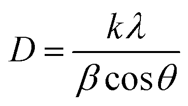 | (1) |
| System | 2θ | d (Å) | R. I. | Integral width (degrees) | Particle size by XRD (nm) | Particle size by TEM (nm) |
|---|---|---|---|---|---|---|
| Y2/3Cu2.90Zn0.10Ti4O12 | 27.5057 | 3.24016 | 15.29 | 0.2356 | 56 ± 6 | 39 ± 6 |
| 30.5396 | 2.92483 | 4.64 | 0.2144 | |||
| 34.4146 | 2.60385 | 100 | 0.2244 | |||
| 36.1312 | 2.48398 | 8.38 | 0.2277 | |||
| 38.6127 | 2.32986 | 7.92 | 0.2106 | |||
| 39.2864 | 2.29144 | 1.39 | 0.1915 | |||
| 41.2920 | 2.18466 | 2.89 | 0.2172 | |||
| 42.4942 | 2.1256 | 6.08 | 0.2122 | |||
| 44.0790 | 2.05278 | 1.13 | 0.1963 | |||
| 46.0575 | 1.9691 | 5.05 | 0.2094 | |||
| 49.4236 | 1.84258 | 30.84 | 0.2143 | |||
| 52.4806 | 1.74221 | 3.04 | 0.2409 | |||
| 54.3804 | 1.68575 | 10.24 | 0.2257 | |||
| 56.7235 | 1.62155 | 2.51 | 0.1983 | |||
| 61.5750 | 1.50491 | 48.9 | 0.2131 | |||
| 62.8522 | 1.47737 | 3.79 | 1.5437 | |||
| 69.0664 | 1.35883 | 3.29 | 0.2248 | |||
| 69.8492 | 1.3455 | 1.55 | 0.1811 | |||
| 72.4406 | 1.30362 | 11.98 | 0.209 |
3.3 Microstructural analysis
Fig. 3 shows the scanning electron micrograph (SEM) of the fractured surface of YCZTO ceramic sintered at 950 °C for 12 h. The SEM micrograph exhibits smooth surfaced grains having bimodal structure with frequent pores. The microstructure is dominated by small spherical, cylindrical and some cubical grains of size 0.5–1.5 μm. The composition of the grains coincides with the stoichiometry of YCZTO, which is also supported by the EDX results. The variation in grain size thereby leading to abnormal grain growth may be owing to the presence of a CuO rich phase in the samples of YCZTO. Fang et al. (2007) also reported the presence of CuO along the grain boundary transforming into liquid phase during sintering. It may instigate a discontinuous grain growth,22 which is in accordance with the SEM micrograph in Fig. 3. The amount of CuO phase as well as an increase in sintering temperature may contribute a significant effect to promote the grain growth and densification of the YCZTO ceramic. Further, the dielectric constant also decreases significantly with grain size having size below 1 μm. It is reported that as the grain size approaches to 0.5–1.5 μm, the various types of stress operating in the grain suppress the domain and the dielectric constant falls to approximately 1000.1 However, there seems to be no such relation between the grain size and dielectric constant value for the YCZTO ceramic. Besides grain size in the range of 0.5–1.5 μm, YCZTO exhibits a higher dielectric constant value (εr ∼ 18![[thin space (1/6-em)]](https://www.rsc.org/images/entities/char_2009.gif) 552) than the pure YCTO ceramic (εr ∼ 8434) with grain size in the range of 1–3 μm, which may be due to porosity, incompactness of the grain and the structural quality of the material.
552) than the pure YCTO ceramic (εr ∼ 8434) with grain size in the range of 1–3 μm, which may be due to porosity, incompactness of the grain and the structural quality of the material.
 | ||
| Fig. 3 SEM micrograph of fractured surface of sintered YCZTO ceramic. | ||
It is also clear from the Fig. 3 that the YCZTO ceramic shows a high degree of porosity. The porosity of the ceramic was measured with the help of the Archimedes principle and was calculated through the following formula:
 | (2) |
An EDX spectrum of grains of sintered Y2/3Cu2.90Zn0.10Ti4O12 ceramic is shown in Fig. 4. It indicates the presence of Y, Cu, Zn, Ti and O elements. Quantitative data for atomic and weight percentage of the elements present in a grain of YCZTO ceramic were obtained from EDX data, which is shown in the inset of the figure. The atomic percentages of Y, Cu, Zn, Ti and O were found to be 4.53, 11.99, 0.43, 18.27 and 64.77, respectively, which is as per the expected stoichiometry of YCZTO ceramic.
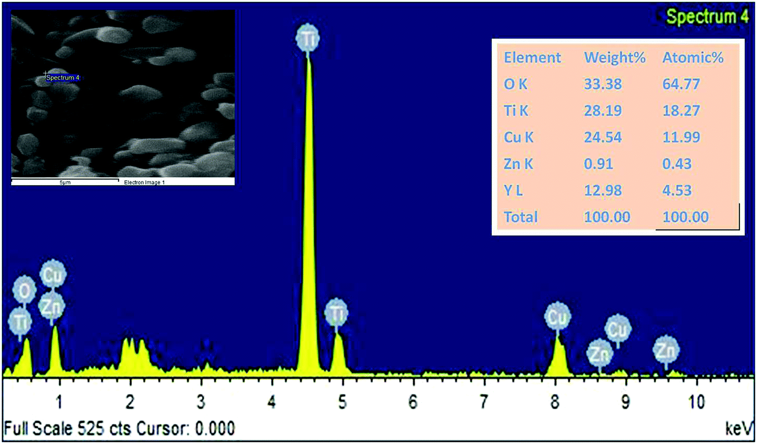 | ||
| Fig. 4 EDX spectrum of a grain surface of sintered Y2/3Cu2.90Zn0.10Ti4O12 ceramic. | ||
The surface topography of Y2/3Cu2.90Zn0.10Ti4O12 ceramic was studied with the help of atomic force microscopy. These images were obtained by a thin film deposition on the glass substrate in tapping mode. AFM study discloses the average roughness (Ra), skewness (Rsk) and kurtosis (Rku). The surface roughness estimated from an AFM image is usually the local roughness of the material. The average roughness is an arithmetic average of the height of the surface asperities, above a hypothetical smooth plane. The skewness shows the degree of symmetry of the rough surface profile and can be used as a measure of the balance between the peaks and valleys of the asperities while the kurtosis shows the degree of sharpness or bluntness of the asperities on the surface. Fig. 5(a) represents the 2-dimensional AFM images of YCZTO, which is characterized by the bright and dark contrast in the grains and shows topological variations, with the brighter regions being higher. Fig. 5(b) shows a two-dimensional AFM image of the grains and grain boundary of YCZTO ceramic. It exhibits a compact structure with granular morphology, buffer layer, plate-like grains and a clear grain boundary. Fig. 5(c) exhibits its 3-dimensional surface morphology and shows several peaks corresponding to grains with compact structure. The maximum peak height of the grains is 3.668 μm within the scanning area of 20 × 20 μm. The average grain size and average grain diameter were estimated to be 90.8 nm (Fig. 6a) and 102.4 nm (Fig. 6b), respectively, out of 301 grains, as exhibited by 3-dimensional AFM histogram, when the grains were homogeneously mounted over the substrate of an area 0.0943 μm2 (Fig. 6c). Fig. 6(d) shows the corresponding surface roughness. Through the roughness parameters, the surface condition of the entire measured length or area will be evaluated in terms of peaks and valleys.24
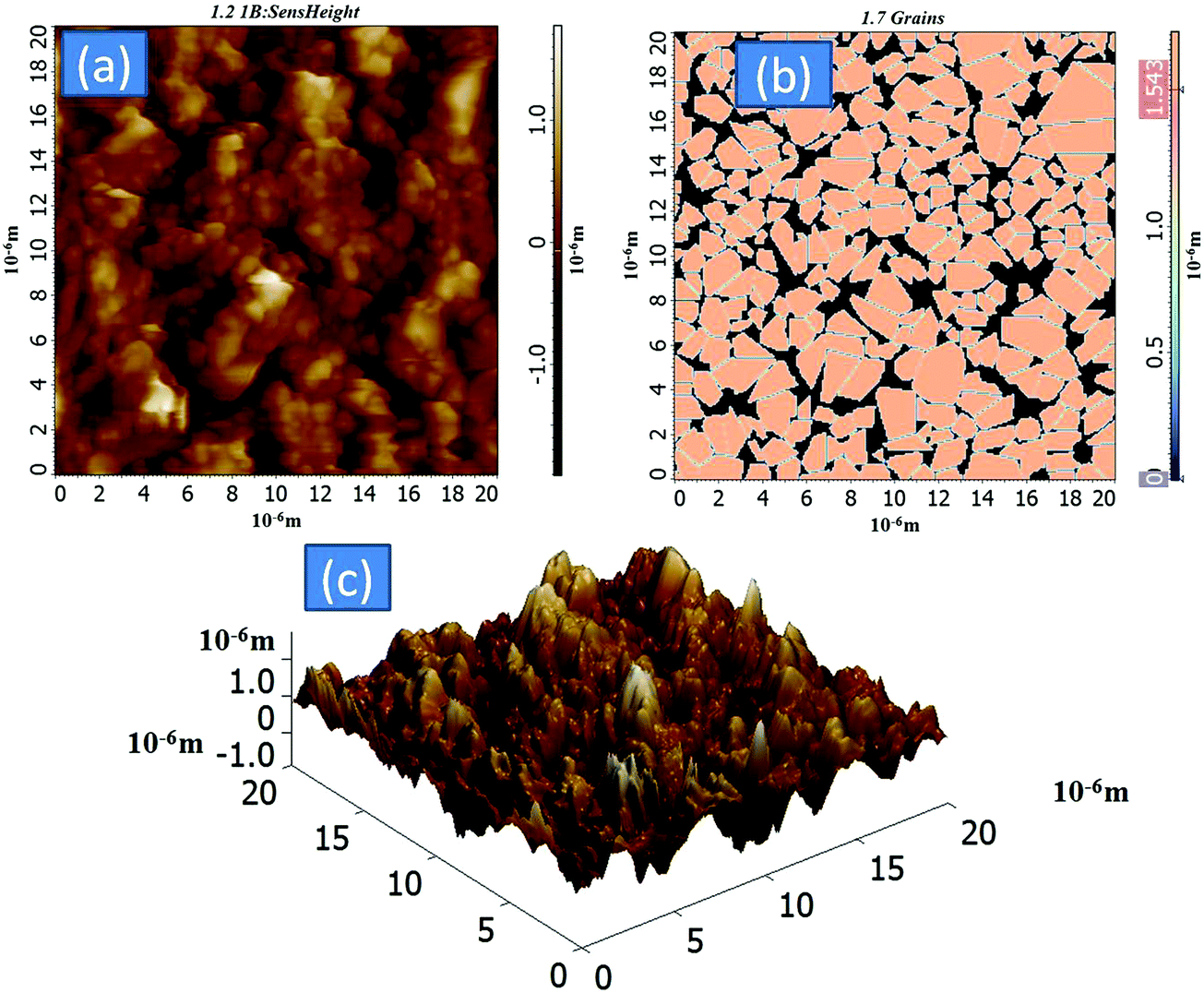 | ||
| Fig. 5 (a) 2-Dimensional AFM micrograph of thin film. (b) 2-Dimensional AFM micrograph showing grain boundary. (c) 3-Dimensional AFM micrograph of sintered Y2/3Cu3−xZnxTi4O12 (x = 0.10) ceramic. | ||
 | ||
| Fig. 6 Different histograms for sintered Y2/3Cu3−xZnxTi4O12 (x = 0.10) ceramic exhibiting (a) average size, (b) diameter of grains, (c) area of grains and (d) average 3-dimensional roughness. | ||
Based upon the statistical study of a total of 65536 grain ensembles, the values of average surface roughness and root mean square roughness were found to be 0.346 and 0.424 μm, respectively within the scanning area of 20 × 20 μm. The skewness was found to be 0.0107, which is nearly equal to zero, and kurtosis to be 3.224, a value exceeding 3. Apart from the average roughness, the lower positive values of skewness roughness (Rsk) imply the smoothness of the surface with predominant peaks while higher positive value for kurtosis roughness (Rku) indicate that the surface of the scanned area of the YCZTO thin film is slightly bumpy in nature owing to the appearance of a low number of high peaks and low valleys on the surface. As the kurtosis value is more than three, such distribution curve has many high peaks and low valleys. It is more evident from the 3-Dimensional AFM image (Fig. 5c). Thus, AFM analysis provides a wider range of particle distribution in the YCZTO ceramic.
The surface roughness parameters of the sample tested in 2-dimensional and 3-dimensional AFM study of YCZTO thin film, obtained by NOVA software, are summarized in Table 2.
| Details of roughness | Parameters | |
|---|---|---|
| Amplitude | Height | |
| Average/arithmetic | 0.261 | 0.366 |
| Root mean square | 0.359 | 0.424 |
| Maximum peak to valley height roughness | 1.943 | 3.672 |
| Ten-points mean height roughness | 1.020 | 3.047 |
| Skewness | 0.0473 | 0.0107 |
| Kurtosis | 3.568 | 3.224 |
The bright field TEM image of YCZTO ceramic sintered at 950 °C for 12 h is represented in Fig. 7(a). The corresponding selected area electron diffraction (SAED) pattern of TEM image is shown in Fig. 7(b). The presence of a few clear rings in the SAED pattern again confirms the formation of the polycrystalline phase of thermodynamically stable YCZTO ceramic. The TEM diffraction pattern was indexed on the basis of a body centred cubic perovskite structure. The lattice parameter calculated from the electron diffraction pattern is also in agreement with the data obtained from XRD. It is clear from Fig. 7(a) that the particles are well dispersed with a high extent of agglomeration. The average particle size is in the range of 39 ± 6 nm. However, the particle size obtained by TEM analysis is less than that from the XRD results because a crystallite may consist of several particles. The concepts of particle size and crystallite size obtained by TEM and XRD are quite different. The measurement of crystallite size is owing to the coherent diffracting crystalline domains (crystallite). One particle can be constituted of several crystalline domains (crystallites), which is why particle size always has to be bigger than crystallite (domain) size or in the case of small nanoparticles, both of them can be the same. However, the domain size or crystallite size, calculated from XRD, cannot be bigger than the particle size obtained from TEM.25
 | ||
| Fig. 7 (a) TEM bright field image and (b) corresponding SAED pattern of YCZTO ceramic sintered at 950 °C for 12 h. | ||
3.4 Ferroelectric study
The origin of the polarization and ferroelectric behaviour of the ceramic may be justified with the help of a polarization electric (PE) loop tracer technique. The PE hysteresis loop is related to its energy storage ability and it displays significant material properties of dielectric materials. This loop can be discussed in terms of three important parameters viz. remnant polarization (Pr), saturated polarization (Ps) and coercive field (Ec) under the external electric field. The PE hysteresis loop obtained at 308 K for YCZTO ceramic is shown in Fig. 8. The values of remnant polarization (Pr), saturation polarization and coercivity (EC) were found to be 0.206 μCcm−2, 0.971 μCcm−2 and 0.477 kV cm−1, respectively. This may be owing to the alignment of domains present in the ceramic, which increases with temperature in the absence of an electric field. Another reason may be the display of high dielectric constant phenomenon, contributing significantly to the relaxor ferroelectric behaviour.26 | ||
| Fig. 8 Polarization hysteresis loop of YCZTO ceramic sintered at 950 °C for 12 h. | ||
3.5 Dielectric study
The effect of temperature on the dielectric constant (ε) and dielectric loss (tan δ) of YCZTO ceramic has been studied in detail. The measurements were carried out in the temperature range of 308–500 K at an interval of 20 degrees. Fig. 9 exhibits the variation of dielectric constant and dielectric loss as a function of temperature for YCZTO ceramic at the selected frequencies of 0.1, 1, 10, and 100 kHz. A slight increase in dielectric constant with temperature is observed in the low frequency range. However, in the higher frequency range (10 kHz and 100 kHz) the dielectric constant is almost temperature independent under the investigated temperature range. At lower frequencies (100 Hz and 1 kHz), characteristic dielectric dispersion peaks were observed below 350 K and thereafter its value increases sharply. At 100 Hz, the value of dielectric constant increases from 886 to 3775 in the temperature range 308 to 327 K and then decreases to 826 at 347 K. However, YCZTO ceramic shows an exceptionally high dielectric constant value (εr ∼2.07 × 10⁴) at 100 Hz and 500 K compared to other frequencies. The dielectric constant exhibits a stepwise increase with increasing temperature beyond the dispersion peak. Such dielectric behaviour is similar to that of CCTO reported earlier by Homes et al.12 An increase in the value of the dielectric constant with an increase in temperature may be attributed to the fact that with an increase in temperature the orientation of the interfacial polarisation is facilitated, thereby enhancing the dielectric constant. However, at lower frequency the rapid increase in dielectric constant with temperature may be owing to the polarisation arising from the orientation of interfacial diploes, which are strongly temperature dependent. As temperature increases, accumulation of charges at the grain boundary increases, thereby inducing an increase in dielectric polarization. Therefore, it is the dielectric polarization that causes an increase in the dielectric constant value with the increase in temperature at lower frequencies. It is also observed from Fig. 9(a) that the value of dielectric constant increases with temperature in contrast to CCTO, which shows almost independent variation with temperature. An increase in the dielectric constant is always accompanied with loss tangent peaks, which signify the presence of high temperature dielectric relaxation in YCZTO ceramic. The high temperature dielectric relaxation may arise from an extrinsic mechanism as well as the presence of defects or oxygen vacancies produced during sintering and cooling mechanisms. The broad dielectric peak obtained for 100 Hz and 1 kHz below 350 K gets suppressed at higher frequency, confirming the presence of ferroelectric relaxor behaviour in the YCZTO.17 Such ferroelectric relaxor behaviour is usually characterized by a diffuse phase transition and strong relaxational dispersion in the dielectric constant and dielectric loss. | ||
| Fig. 9 Plots of dielectric constant (ε′) and loss tangent (tan δ) vs. temperature at a few selected frequencies for sintered YCZTO ceramic. | ||
The variation of dielectric loss (tan δ) as a function of temperature shown in Fig. 9(b) is characterized by the presence of the same type of dispersion peaks below 350 K. The dielectric losses for YCZTO ceramic at 350 K were found to be 0.47, 0.32, 0.10, and 0.02 at 0.1, 1, 10, and 100 kHz, respectively. The presence of dispersion peaks in both the figures below 350 K and at lower frequencies (i.e. less than 1 KHz) indicated the presence of Debye type relaxation behaviour in the ceramic. The presence of low frequency relaxation may be attributed to the occurrence of space charge polarization arising at the interface of the grain and the grain boundary having a large difference in their electrical conductivity. It is clearly seen that the value of tan δ increases with increases in temperature. A rapid increase in tan δ at higher temperatures is owing to an exponential increase of conductivity with temperature, as observed normally.
Fig. 10 illustrates the frequency dependence of ε′ of sintered YCZTO ceramic at a few selected temperatures. It is clearly observed that the dielectric constant decreases gradually with increased frequency. This decrease is more prominent in the low frequency region, which may be explained in terms of relaxation of dipoles at the grain boundary as well as owing to the contribution of interfacial effects resulting from the ceramic–electrode combination. The value of ε′ for YCZTO ceramic was found to be 18552 at 308 K and 100 Hz while the undoped YCTO ceramic exhibited a dielectric constant of 8434 at the same temperature and frequency, a value much higher than for the undoped one. It is also clear that the dielectric constant (ε′) decreases steeply in the lower frequency range whereas it decreases slowly in the higher frequency range (1 kHz–5 MHz). The decrease in dielectric constant with frequency may be owing to the contribution of space charge accumulation at the interface, which leads to polarization of the ionic medium and hence increases the value of ε′. In high frequency regions, the periodic reversal of the field takes place so rapidly that there is no charge accumulation at the interface, resulting in a constant ε′ value.27
 | ||
| Fig. 10 Plots of real part of dielectric constant (ε′) with frequency at different temperatures for sintered YCZTO ceramic. | ||
Apart from the values of ε′ and tan δ, the temperature coefficient (Δε′), is one of the most important parameters. It predicts the compatibility of any desired material for appropriate capacitor and resonator applications. The temperature coefficient (Δε′) for YCZTO ceramic was calculated at a frequency of 1 kHz and may be defined as 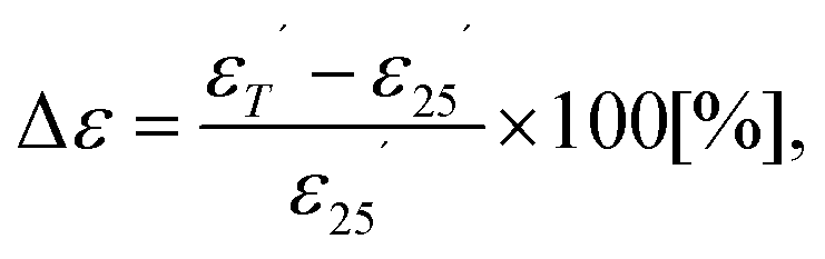 where ε′ and ε′ are the values of the real part of the dielectric constant (ε′) at temperatures T °C and 25 °C, respectively. The calculated value of Δε′ was lower than 15% in the temperature range 308–500 K, thereby indicating the potential use of YCZTO ceramic as a capacitor device.
Dielectric absorption in a material is generally characterized by tan δ as well as dielectric loss (ε′′) values. Usually a relaxation peak is obtained when ε′′ and tan δ values are plotted against frequency. Such dielectric relaxation occurs when the hopping frequency of charge carriers equals the frequency of the applied field. Such relaxation peaks were absent in the case of YCZTO ceramic when the imaginary part of the dielectric constant (ε′′) is plotted against frequency, as shown in Fig. 11. However, undoped YCTO ceramic gives direct evidence for relaxor behaviour exhibiting corresponding relaxation peaks around 105–106 Hz. The absence of relaxation peaks in YCZTO ceramic may be attributed to the reduction in the number of hoppings as the concentration of Zn increases. It is likely that the relaxation peaks corresponding to YCZTO ceramic may lie outside the measured frequency range.
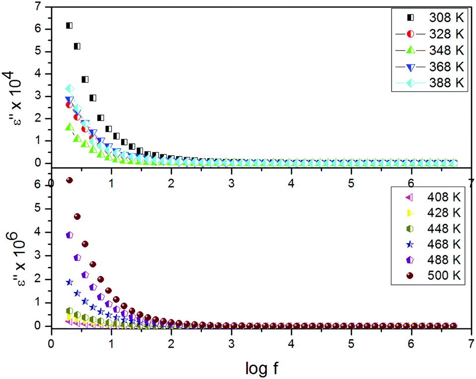 | ||
| Fig. 11 Plots of imaginary pat of dielectric constant (ε′′) with frequency at different temperatures for sintered YCZTO ceramic. | ||
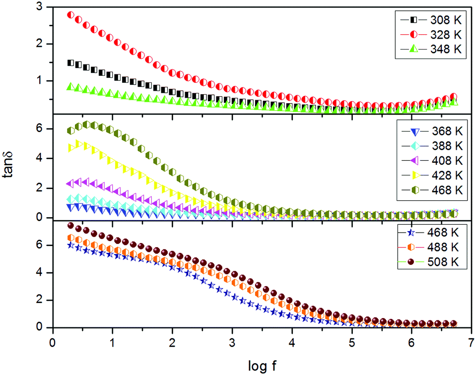
Fig. 12 shows the variation of loss tangent (tan δ) with frequency at a few selected temperatures (308–500 K) and is characterized by the presence of relaxation peaks. These peaks shift to higher frequency regions with increase in temperature, indicating the presence of Debye type Maxwell–Wagner relaxation. YCZTO ceramic shows the minimum dielectric loss (tan δ ∼ 0.76) at 368 K with corresponding dielectric constant value ε ∼ 7183 at 2 Hz. The dielectric loss of YCZTO ceramic was found to be 0.2 to 1.03 (308 to 428 K) and 2.3–3.38 (468–500 K) at 1 kHz. The dielectric loss in a low frequency region may be attributed to the conduction of oxygen vacancies originated by mass diffusion during the sintering process but slight increases in tan δ with frequency may be caused owing to high conductivity associated with the grain boundary. It implies that the grain boundary, in this condition, becomes an insulator. The insulating nature of the grain boundary may be attributed to the sintering effects and its conditions. Normally oxygen diffusion takes place during sintering owing to the difference in the partial pressure of oxygen in the ceramic oxide and the atmosphere. As the grain boundary is associated with a higher diffusion coefficient, the rate of oxygen diffusion is usually more at the grain boundary in comparison to in the grain and, in turn, the extent of reoxidation is more at the grain boundary during the process of cooling. These effects may lead to a semiconducting grain and an insulating grain boundary in YCZTO ceramic, like several oxide ceramics, and supports the IBLC mechanism.
 | ||
| Fig. 12 Plots of loss tangent (tan δ) vs. frequency at a few selected temperatures for sintered YCZTO ceramic. | ||
3.6 Impedance spectroscopic studies
The electrical behaviour of YCZTO ceramic has been characterized over a wide range of frequency and temperature by employing the complex impedance (Z*) to disclose the reasons for dielectric dispersion and formation of the barrier layer in YCZTO ceramic as well as the presence of multi-polarization processes appearing simultaneously in the ceramic with their usual relaxation conditions. In polycrystalline materials, impedance formalism emphasizes grain boundary conduction effects while bulk effects dominate in the electric modulus formalism.The Nyquist plot between Z′ and Z′′ of sintered YCZTO ceramic at a few selected temperatures is shown in Fig. 13. It is quite clear from the graph that all the curves exhibit a common tendency to bend towards the abscissa to form semicircles with their centres below the real axis. Fig. 13 is further characterized by the presence of a single semi-circular arc at 308–500 K. However, in the low frequency region, the complex impedance plot at 468–500 K neither shows the complete semicircle nor any characteristic electrode spike; rather, a long residual tail exists. It may be due to the grain boundary or electrode surface effects, or both, depending upon the temperature. The absence of an electrode-spike indicates that the material is an electronic conductor in the non-ferroelectric orientation at 308–448 K. The semi-circular arc corresponding to grain at high frequency has been suppressed due to the high value of grain boundary resistance, which is analogous to internal barrier layer capacitance (IBLC), characterized by a semiconducting grain with an insulating grain boundary.
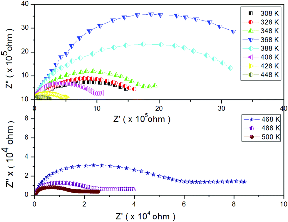 | ||
| Fig. 13 Plots of complex impedance plane plots (Z′ vs. Z′′) at a few selected temperatures for sintered YCZTO ceramic. | ||
On extrapolation in the high frequency region, the intercept on the Z′ axis (in Fig. 13) is not found to be close to zero, suggesting that there must be the existence of another semi-circle in the high frequency region beyond the measuring frequency range. The non-zero intercept of the arc passing through the origin on the Z′ axis gives the effective contribution of the grain resistance (Rg) value, while that of the another arc in the lower frequency range gives the contribution of grain boundaries (Rgb) to the total resistance. The calculated values of Rg and Rgb are listed in Table 3. It is also observed that the radii corresponding to the sizes of different arcs are decreasing with increasing temperature, thereby representing the distribution of relaxation times in the YCZTO ceramic and indicating a decrease in the resistivity of the material with the increase in temperature. It is also clear from the table that grain boundary resistance decreases with increasing temperature, whereas grain resistances do not much alter with temperature, confirming the semiconducting behaviour of grains. From Table 3, it can also be inferred that the resistance of the grain boundary is very high in comparison to those of the grains, and thus the grains behave as an insulator.
| Temp. (K) | R g (Ω) | R gb (Ω) | C g (pF) | C gb (nF) |
|---|---|---|---|---|
| 308 | 347 | 1.70 × 10⁶ | — | — |
| 328 | 292 | 1.84 × 10⁶ | — | — |
| 348 | 296 | 1.98× 10⁶ | — | — |
| 368 | 302 | 4.48 × 10⁶ | — | — |
| 388 | 271 | 3.52 × 10⁶ | — | — |
| 408 | 271 | 1.03 × 10⁶ | — | 5.25 |
| 428 | 239 | 0.49 × 10⁶ | — | 4.59 |
| 448 | 241 | 0.22 × 10⁶ | — | 4.40 |
| 468 | 206 | 0.06 × 10⁶ | — | 4.10 |
| 488 | 122 | 0.02× 10⁶ | — | — |
| 500 | 60 | 0.01× 10⁶ | — | 3.80 |
The variation of the imaginary part of impedance Z′′ with frequency at a few selected temperatures, shown in Fig. 14, exhibits relaxation peaks at all measured temperatures. The decrease in magnitudes of Z′′ with increase in frequency implies that relaxation in YCZTO material is highly temperature-dependent and apparently there is no single relaxation time. A significant broadening of relaxation peaks with the rise in temperature again confirms the existence of a temperature-dependent electrical relaxation phenomenon in the material. The asymmetric broadening of peaks in YCZTO ceramic also suggests the presence of electrical phenomena with a wide spread of relaxation time. The factors responsible for relaxation behaviour in YCZTO ceramic may possibly be the presence of immobile species or electrons at low temperature and defects or vacancies at higher temperature. The localized relaxation in dielectric materials originating from defect relaxation dominates because of the low dielectric ratio = εs/ε∞, where εs and ε∞ are dielectric constants at low and high frequencies, respectively. Dispersion of the resultant curves in the low frequency region at different temperatures is very clear and it appears to be merging at higher frequency, irrespective of temperature variations in YCZTO. Such behaviour is owing to the presence of the space charge polarization effects at lower frequency but at higher frequency, it gets eliminated.28
 | ||
| Fig. 14 Plots of Z′′ vs. frequency at a few selected temperatures for sintered YCZTO ceramic. | ||
Furthermore, these peaks get suppressed but slightly shifted to the high frequency region with increasing temperature, thereby indicating the possible release of space charge accumulation at the boundaries of homogeneous phases in the test material under the applied external field. All this evidence supports the existence of a temperature-dependent Maxwell–Wagner dielectric relaxation.
3.7 Modulus spectroscopic studies
The presence of long-range conduction phenomenon as well as different types of microscopic processes responsible for localized dielectric relaxations in YCZTO ceramics were investigated separately by modulus spectroscopic studies. The temperature-dependent Cole–Cole plot between M′ and M′′ shown in Fig. 15 clearly indicates the presence of semicircles for each temperature (from 308 to 500 K) having their centre below the real axis, suggesting the presence of grain boundaries along with the grains in YCZTO ceramic. The Cole–Cole plot also justifies a poly-dispersive nature for the dielectric relaxation at low frequencies. These observations are related to the lack of resorting force governing the mobility of charge carriers under the action of an induced electric field. This behaviour supports the long range mobility of charge carriers. | ||
| Fig. 15 Plots of electric modulus plots M′ vs. M′′ at a few selected temperatures for sintered YCZTO ceramic. | ||
In order to explain the modulus spectra of YCZTO ceramic, the variation of the imaginary part of electric modulus (M′′) is plotted against frequency at a few selected temperatures and is shown in Fig. 16. These curves exhibit the presence of well-defined relaxation peaks. The presence of a relaxation peak in the higher frequency region may be due to the grain. The relaxation peaks due to grain and grain boundary responses usually occur at frequencies 1/(2πRgCg) and 1/(2πRgbCgb), respectively. As the peak values are proportional to the reciprocal of the associated capacitance, the smallest capacitance will dominate in the electric modulus plots. The grains usually have smaller capacitances than the grain boundaries as their peaks are stronger in the modulus spectra. The capacitance of the grain boundary was also calculated from the plot and is recorded in Table 3. It is observed that the height of all the relaxation peaks (Fig. 16) is not constant; rather, it keeps on increasing with temperature. which indicates a decreasing trend in capacitance.
 | ||
| Fig. 16 Plots of M′′ vs. frequency at a few selected temperatures for sintered YCZTO ceramic. | ||
Furthermore, the frequency region below the relaxation peak determines the range in which charge carriers are mobile over long distances at a particular temperature. At frequencies above fmax, the charge carriers are mobile over short distances as they remain confined to their potential wells. Again, the relaxation peaks shift to the higher frequency region with increasing temperature, providing direct evidence for temperature dependent relaxation. This behaviour also suggests that the dielectric relaxation in YCZTO ceramic is thermally activated.28
3.8 Magnetic study
The magnetic behaviour of the ceramic was studied under ZFC and FC conditions. Fig. 17 depicts the ZFC and FC magnetization curves obtained at an applied field of 100 Oe for YCZTO ceramic sintered at 950 °C at The variation of the MZFC and MFC curves is characterized by a gradual increase in both the curves with decreasing temperature until the corresponding peaks are obtained at 25 K. At higher temperature, both curves show a sharp decrease with a tail, which is analogous to superparamagnetic materials. Furthermore, the MFC curve overlaps with the MZFC curve at higher temperature but splits from the MZFC curve below the bifurcation temperature Tb = 148 K, below which the ZFC and FC moments show different branches and above which the two branches get merged into a tail, extending up to the Curie temperature (Tc). It can be obtained by the extrapolation of the linear part giving the x-intercept in the temperature axis. The Curie temperature for YCZTO ceramic was found to be 201 K.29 | ||
| Fig. 17 Temperature dependence of zero field cooled (ZFC) and field cooled (FC) magnetisation at an applied field of 100 Oe in YCZTO ceramic. | ||
Both MZFC and MFC curves decrease below their peak temperatures of 25.70 and 23.92 K, respectively and they are almost parallel, thereby suggesting a common phenomenon is responsible for the shape of the curve. Again, a sharp increase in the values of MZFC and MFC above temperatures of 8.25 and 9.46 K is observed, respectively. This discrepancy in the MZFC and MFC data of the sharp increase may be owing to the presence of a ferromagnetic component in the YCZTO ceramic corresponding to some structural and magnetic changes within the YCZTO ceramic.30
Fig. 18 exhibits the linear variation of magnetic moment with magnetic field, confirming its paramagnetic phase in YCZTO ceramic. Furthermore, we found that the hysteresis loop exhibits a high coercive field value. It is dependent on the strength of the external field at which the sample was cooled, rate of cooling, and the lowest temperature. This phenomenon indicates that the crystal particles have a strong anisotropy field so that the maximum applied field was not enough to close the loop, resulting in the observed minor loop characteristics. In fact, at low temperatures the crystalline powder exhibits features that may be related to the magnetic canting in the antiferromagnetic state.31 A non-saturated hysteresis loop was obtained at the magnetic moment ±10.63 emu with coercivity-field value +10.63 Oe, which is clearer from the top inset of Fig. 18 showing coercivity between the field ±20 Oe and the remnant magnetization of 5.86 × 10⁶ emu for YCZTO ceramic. The presence of such a non-saturated hysteresis loop also suggests the phase transition from paramagnetic to superparamagnetic.
 | ||
| Fig. 18 Magnetisation versus magnetic field hysteresis (M–H) curve at 300 K for YCZTO ceramic. The inset shows an enlarged view of M–H curve at low fields. | ||
4. Conclusions
Nano-sized Y2/3Cu2.90Zn0.10Ti4O12 ceramic was synthesized by semi-wet route and its dielectric properties were studied as a function of frequency and temperature. Single phase formation along with the presence of a secondary phase of CuO of the ceramic was confirmed by XRD characterization. The crystallite size of the YCZTO ceramic was found to be 56 ± 6 nm by XRD while TEM studies revealed the size of agglomerated particles to be 39 ± 6 nm. Microstructure with normal grain growth was observed in YCZTO ceramic. A giant value of εr of about 1.8 × 10⁴ at room temperature was obtained and was attributed to the heterogeneous microstructure of semiconducting grains and insulating grain boundaries. With increasing temperature, the dielectric constant and dielectric loss increased. The impedance studies of YCZTO ceramic showed two major contributions associated with the grain boundaries and electrode effect. The resistance of grain boundaries appeared as a major contribution at higher temperature and electrode resistance appeared at low temperature owing to electrode polarization. The asymmetric broadening of peaks in YCZTO ceramic also suggested the presence of electrical phenomena with a wide spread of relaxation time. Impedance and modulus analyses of YCZTO ceramic confirmed the presence of temperature-dependent Maxwell–Wagner type of relaxation. Magnetic study suggested the presence of a paramagnetic to superparamagnetic phase transition in the YCZTO ceramic, which may correspond to any structural and magnetic changes within the YCZTO ceramic.Acknowledgements
The authors are thankful to Prof. R. K. Mandal, Department of Metallurgical Engineering, I. I. T. (B. H. U.) for extending the TEM and SEM facility.References
- A. J. Moulson and J. M. Herbert, Electroceramics, 2nd edn, Wiley, England, 2003, pp. 243–329 DOI:10.1002/0470867965.ch4.
- D. E. Kotecki, Integr. Ferroelectrics, 1997, 16, 1–9, DOI:10.1080/10584589708013025.
- R. J. Cava, Dielectric materials for applications in microwave communications, J. Mater. Chem., 2001, 11, 54–62, 10.1039/B003681L.
- C. M. Garner, G. Kloster, G. Atwood, L. Mosley and A. C. Palanduz, Challenges for dielectric materials in future integrated circuit technologies, Microelectron. Reliab., 2005, 45(5), 919–924, DOI:10.1016/j.microrel.2004.11.053.
- H. Yu, H. Liu, H. Hao, L. Guo and C. Jin, Grain size dependence of relaxor behavior in CaCu3Ti4O12 ceramics, Appl. Phys. Lett., 2007, 91, 222911, DOI:10.1063/1.2820446.
- M. A. Subramanian, D. Li, N. Duan, B. A. Reisner and A. W. Sleight, High Dielectric Constant in ACu3Ti4O12 and ACu3Ti3FeO12 Phases, J. Solid State Chem., 2000, 151, 323–325, DOI:10.1006/jssc.2000.8703.
- M. A. Subramanian and A. W. Sleight, ACu3Ti4O12 and ACu3Ru4O12 perovskites: high dielectric constants and valence degeneracy, Solid State Sci., 2002, 4, 347–351, DOI:10.1016/S1293-2558(01)01262-6.
- A. P. Ramirez, M. A. Subramanian, M. Gardel, G. Blumberg, D. Li, T. Vogt and S. M. Shapiro, Giant dielectric constant response in a copper-titanate, Solid State Commun., 2000, 115, 217–220, DOI:10.1016/S0038-1098(00)00182-4.
- D. C. Sinclair, T. B. Adams, F. D. Morrison and A. R. West, CaCu3Ti4O12: one-step internal barrier layer capacitor, Appl. Phys. Lett., 2002, 80, 2153–2155, DOI:10.1002/1521-4095(20020916)14:18.
- P. Lunkenheimer, R. Fichtl, S. G. Ebbinghaus and A. Loidl, Nonintrinsic Origin of the Colossal Dielectric Constants in CCTO, Phys. Rev. B: Condens. Matter Mater. Phys., 2004, 70, 172102, DOI:10.1103/PhysRevB.70.172102.
- M. H. Cohen, J. B. Neaton, L. X. He and D. Vanderbilt, Extrinsic models for the dielectric response of CaCu3Ti4O12, J. Appl. Phys., 1967, 18, 37–40, DOI:10.1063/1.1595708.
- C. C. Homes, T. Vogt, S. M. Shapiro, S. Wakimoto and A. P. Ramirez, Optical Response of High Dielectric Constant Perovskite-Related Oxide, Science, 2001, 293, 673–676 CrossRef CAS PubMed.
- L. Jianjun, D. Chun Gang, W. N. Mei, R. W. Smith and J. R. Hardy, Dielectric properties and Maxwell-Wagner relaxation of compounds ACu3Ti4O12 (A = Ca, Bi2/3,Y2/3,La2/3), J. Appl. Phys., 2005, 98, 093703, DOI:10.1063/1.2125117.
- K. D. Mandal, R. A. Kumar, D. Kumar and O. Parkash, Dielectric properties of the Ca1−xLaxCu3Ti4−xCoxO12 system (x = 0.10, 0.20 and 0.30) synthesized by semi-wet Route, J. Alloys Compd., 2009, 478, 771–776, DOI:10.1016/j.jallcom.2008.12.007.
- P. F. Liang, Z. P. Yang, X. L. Chao and Z. H. Liu, Giant Dielectric Constant and Good Temperature Stability in Y2/3Cu3Ti4O12 Ceramics, J. Am. Ceram. Soc., 2012, 95(7), 2218–2225, DOI:10.1111/j.1551-2916.2012.05152.x.
- L. Junwei, P. F. Liang, Y. Jing, C. Xiaolian and Y. Zupei, Phase Formation and Enhanced Dielectric Response of Y2/3Cu3Ti4O12 Ceramics Derived from the Sol–Gel Process, J. Am. Ceram. Soc., 2015, 98(3), 795–803, DOI:10.1111/jace.13355.
- S. Sunita, Y. S. Sundar, M. M. Singh and K. D. Mandal, Impedance spectroscopic and dielectric properties of nano-sized Y2/3Cu3Ti4O12 ceramic, J. Adv. Dielectr., 2014, 4, 1450030, DOI:10.1142/ S2010135X14500301.
- S. Sharma, M. M. Singh, U. S. Rai and K. D. Mandal, Rationalization of dielectric properties of nano- sized iron doped yttrium copper titanate using impedance and modulus studies, Mater. Sci. Semicond. Process., 2015, 31, 720–727, DOI:/10.1016/j.mssp.2014.12.069.
- P. Liang, X. Chao, F. Wang, Z. Liu and Z. Yang, The Lowered Dielectric Loss and Grain-Boundary Effects in La-doped Y2/3Cu3Ti4O12 Ceramics, J. Am. Ceram. Soc., 2013, 96, 3883–3890 CrossRef CAS.
- P. Liang, X. Chao and Z. Yang, Low dielectric loss, dielectric response, and conduction behavior in Na- doped Y2/3Cu3Ti4O12 ceramics, J. Appl. Phys., 2014, 116, 044101 CrossRef.
- B. D. Culity and S. R. Stock, Elements of X-ray Diffraction, Prentice Hall, New Jersey, 2001, ch. 1 Search PubMed.
- T. T. Fang and C. P. Liu, Evidence of Cu Deficiency: A Key Point for the Understanding of the Mystery of the Giant Dielectric Constant in CaCu3Ti4O12, J. Am. Ceram. Soc., 2007, 90, 638–640 CrossRef CAS.
- E. Niwa, C. Uematsu and T. Hashimoto, Evaluation of Specific Surface Area and Pore Size Distribution of LaNi0.6Fe0.4O3 Ceramics Prepared using Pechini Method by N2 Adsorption Method—Optimization of Sintering Temperature as Cathode Material of Solid Oxide Fuel Cells, J. Am. Ceram. Soc., 2012, 95, 3802–3810, DOI:10.1111/jace.12022.
- M. Raposo, Q. Ferreira and P. Ribeiro, Modern Research and Educational Topics in Microscopy: A Guide for Atomic Force Microscopy Analysis of Soft Condensed Matter, Condens. Matter, 2007, 758–763 Search PubMed.
- D. B. Williams and C. Barry Carter, T. E. M.: A. Textbook for Materials Science, 2nd edn, Springer, US, 2009, pp. 23–38 Search PubMed.
- S. C. Raya, S. K. Bhunia, A. Saha and N. Jana, Graphene oxide (GO)/reduced-GO and their composite with conducting polymer nanostructure thin films for non-volatile memory device, Microelectron. Eng., 2013, 146, 48–52, DOI:10.1016/j.mee.2015.04.001.
- B. Tareev, Physics of Dielectric Materials, Mir Publication, Moscow, 1975, pp. 35–39 Search PubMed.
- D. B. Dhawajam, M. Buchi Suresh, U. S. Hareesh, J. K. Thomas, S. Solomon and A. John, Impedance and Modulus spectrocscopic studies on 40 PrTiTaO6 + 60YTiNbO6 ceramic composite, J. Mater. Sci.: Mater. Electron., 2012, 23, 653–661, DOI:10.1007/s 10854-011-0464.
- D. Kumar, P. Mohanty, V. P. Singh, K. Jagadish, G. A. Banerjee, V. Ganesan and C. Rath, Tuning of magnetic transition temperatures in nanoparticles of CoCr2O4 multiferroic by B-site mixing, Mater. Res. Bull., 2014, 54, 78–83 CrossRef CAS.
- G. Anandha Babu, G. Ravi, Y. Hayakawa and M. Kumaresavanji, Synthesis and calcinations effects on size analysis of Co3O4 nanospheres and their superparamagnetic behaviors, J. Magn. Magn. Mater., 2015, 375, 184–193 CrossRef CAS.
- H. Khurshid, W. Li, M. H. Phan, P. Mukherjee, G. C. Hadjipanayis and H. Srikanth, Surface spin disorder and exchange-bias in hollow maghemite nanoparticles, Appl. Phys. Lett., 2012, 101, 022403 CrossRef.
| This journal is © the Partner Organisations 2017 |