
 Open Access Article
 This Open Access Article is licensed under a Creative Commons Attribution-Non Commercial 3.0 Unported Licence
Optical detection of charge dynamics in CH3NH3PbI3/carbon nanotube composites†
Hajnalka M.
Tóháti
a,
Áron
Pekker
 *a,
Pavao
Andričević
b,
László
Forró
b,
Bálint
Náfrádi
b,
Márton
Kollár
b,
Endre
Horváth
b and
Katalin
Kamarás
a
*a,
Pavao
Andričević
b,
László
Forró
b,
Bálint
Náfrádi
b,
Márton
Kollár
b,
Endre
Horváth
b and
Katalin
Kamarás
a
aInstitute for Solid State Physics and Optics, Wigner Research Centre for Physics, Hungarian Academy of Sciences, 1525 Budapest, Hungary. E-mail: pekker.aron@wigner.mta.hu
bLaboratory of Physics of Complex Matter (LPMC), Ecole Polytechnique Fédérale de Lausanne, 1015 Lausanne, Switzerland
First published on 27th September 2017
Abstract
We have investigated the optical absorption of metallic and semiconducting carbon nanotubes/CH3NH3PbI3 micro- and nanowire composites. Upon visible light illumination semiconducting carbon nanotube based samples show a photo-induced doping, originating from the charge carriers created in the perovskite while this kind of change is absent in the composites containing metallic nanotubes, due to their strikingly different electronic structure. The response in the nanotubes shows, beside a fast diffusion of photo-generated charges, a slow component similar to that observed in pristine CH3NH3PbI3 attributed to structural rearrangement, and leading to slight, light induced changes of the optical gap of the perovskite. This charge transfer from the illuminated perovskite confirms that carbon nanotubes (especially semiconducting ones) can form efficient charge-transporting layers in the novel organometallic perovskite based optoelectronic devices.
1. Introduction
Third generation photovoltaic devices have recently generated great interest because of their low cost and high efficiency potential. Organic–inorganic metal halide perovskites, especially methylammonium lead iodide (CH3NH3PbI3, henceforth referred to as MAPbI3), emerged as front runners in this generation due to their excellent optoelectronic properties such as high absorption coefficient, high mobility, long and balanced carrier diffusion and low exciton binding energy.1–5 These perovskite solar cells have achieved efficiencies above 20%6,7 within a period shorter than any other material proposed for solar energy conversion. They are approaching the efficiency of commercial c-Si solar cells. However, there are still shortcomings that prevent these cells from getting to the market, one being the high cost and the other being stability issues of the hole-selective transport layer (HTM) in the cell. The most common HTM material, with which the highest power conversion efficiencies have been obtained, is 2,2′,7,7′-tetrakis(N,N-di-p-methoxyphenyl-amine)9,9′-spirobifluorene (Spiro-OMeTAD).8Recently, carbon nano-materials, such as nanoparticles, carbon nanotubes (CNTs) and graphene flakes, are being reported as good alternatives for HTM materials.9–13 In particular, CNTs are very attractive candidates, since they have been already used successfully in various optoelectronic applications, like light-emitting diodes, photodetectors, phototransistors14,15 and other photovoltaic cells, due to their direct band gap (when they are semiconducting) and outstanding electronic and mechanical properties.16 Not only did they show comparable performance to conventional architectures, but they also provided devices with improved features such as stability, reduction of the hysteretic and drift effects,17,18 flexibility19 and semi-transparency.20 Therefore, to be able to increase further the performance of perovskite–CNT based devices it is important to learn more about the interface between perovskites and different types of CNTs. In particular, it is essential to understand the details of the charge transfer from the illuminated photovoltaic perovskite to the CNTs.
Several studies of the subject have already been published,9,21,22 strongly suggesting photoinduced charge transfer between CNTs and perovskites that leads to mobile charge carriers in the system. These studies were mainly based on the bleaching of the first excitonic optical transition (S11) of semiconducting nanotubes. The presence of mobile carriers was concluded from photocurrent measurements9 and from time-resolved microwave conductivity at 9 GHz.22 Charge transfer between the CNTs and the perovskite layer was further inferred from photoemission spectroscopy21 and the dynamics of the process was determined on a timescale less than a millisecond. All these measurements were conducted in device architectures, thus reflecting the processes of all layers and interfaces.
In this work we use a simple MAPbI3/CNT hybrid system in order to restrict our observations to the one interface between these constituents, and extend the study of charge transport to longer wavelengths and longer timescales. We report the charge transfer between MAPbI3 and CNTs upon white light illumination by using mid-infrared (MIR) and near-infrared (NIR) optical spectroscopy. In the MIR range, we follow the appearance upon illumination of free-carrier (Drude) absorption, correlated with the photobleaching of the S11 transition in the NIR, thus establishing the charge migration through the interface as the source of photocurrent under operating conditions of solar cells. The dynamics of the process extends to the timescale of tens of minutes, connecting the charge migration to structural changes in the perovskite.23–25 A comparison between two high purity nanotube samples is given in order to illustrate the difference between semiconducting and metallic nanotube enriched samples. We find that semiconducting nanotubes show a distinct advantage over metallic nanotubes regarding photoinduced charge transport, confirming the choice of previous studies to apply semiconducting21,22 or functionalized9 carbon nanotubes in similar architectures. Furthermore, we prove that there is no severe chemical reaction establishing covalent bonds between the nanotubes and the perovskite during the synthesis of the composite system. The processes studied here can form the basis of further possible optoelectronic applications of the MAPbI3-semiconducting nanotube ensemble beyond solar cells, mentioned above.
2. Experimental methods
High purity commercially available single-walled carbon nanotube samples (NanoIntegris Inc.) were used in this study, prepared from arc-derived carbon nanotubes (mean diameter: 1.4 nm) by density gradient ultracentrifugation.26 Two different types of samples were investigated: one batch was enriched with 95% semiconducting (s-CNTs) and another with 95% metallic (m-CNTs) nanotube content. Spectroscopy studies were carried out on self-supporting nanotube thin films. Preparation of the nanotube samples was done by vacuum filtration and wet transfer.27 The thin films were annealed at 200 °C in a vacuum for 10 hours to remove moisture and solvent residues. MAPbI3 single crystals were prepared according to Poglitsch and Weber.28 The harvested single crystals were dissolved in N,N-dimethylformamide. The concentration of the solution was 114 mg ml−1. The composite CNT/MAPbI3 samples were prepared by drop casting a 4 μl solution of MAPbI3 in N,N-dimethylformamide (DMF) on self-supporting CNT films, resulting in micrometer-sized wires described earlier.15,29 The composite samples were dried in air for 30 min at 80 °C.The possible chemical reaction at the CNT/MAPbI3 interface was excluded by Raman measurements, since the D and G bands did not change with respect to the pristine CNTs (ESI, Fig. S1†). The samples were characterized by mid-infrared (MIR) and near-infrared (NIR) spectroscopy techniques. The MIR and NIR measurements were performed in a dry nitrogen purged Bruker Tensor 27 FTIR spectrometer. For illumination a 3 W white light emitting diode (LED) was used. In order to cut off the high energy part of the LED light, a 500 nm long-pass filter was used. The samples were kept in the dark before the measurements and illuminated only with the LED light. SEM images were taken with a Quanta 3D (FEI) scanning electron microscope using a backscattered electron detector and an LVEM5 (Delong America Inc.) electron microscope using a secondary electron detector.
3. Results and discussion
Typical images of the composite samples are summarized in Fig. 1. Fig. 1a shows the optical image of the sample where the micrometer-wide wires of MAPbI3 are supported by the CNT film. It is likely that such a texture of the perovskite is caused by the solvent and/or by the CNT substrate. Fig. 1b shows a scanning electron microscopy (SEM) image of a similar CNT/MAPbI3 sample. This image was taken using a backscattered electron detector which enables good resolution on the pristine carbon nanotube network (dark gray regions) but fails to capture the details of the MAPbI3 crystals (bright regions). To complement this limitation we have taken another image with a similar magnification using a secondary electron detector showing the MAPbI3 crystals formed on the nanotube mat (Fig. 1c). These nanocrystals are similar in size (10–50 nm) to what has been found in perovskite/CNT hybrid materials reported by Ka et al.30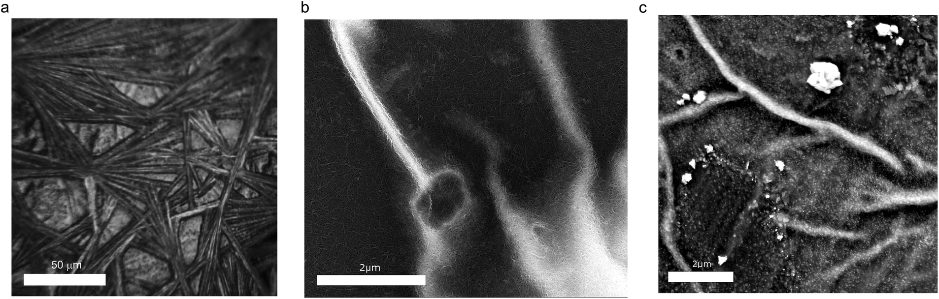 | ||
| Fig. 1 (a) Optical image of a (mixed s–m) CNT/MAPbI3 composite prepared for measurement (the scale bar is 50 μm). First, elongated micro- and nanocrystallites of MAPbI3/DMF solvatomorph precursor phase were grown. The MAPbI3 wires were formed by subsequent solvent evaporation, while preserving the elongated crystal shape. These wires are placed on a 100 nm thick dense mat of self-supporting carbon nanotubes. (b) SEM image of MAPbI3/DMF drop cast on a CNT film recorded by using a backscattered electron detector (good resolution for CNT, limited resolution for MAPbI3, the scale bar is 2 μm). (c) SEM image of MAPbI3/DMF drop cast on a CNT film recorded by using a secondary electron detector (limited resolution for CNT, good resolution for MAPbI3, scale bar is 2 μm). | ||
To investigate the effect of visible light illumination on the nanotube–MAPbI3 composite samples we performed spectroscopic measurements in the 500–15![[thin space (1/6-em)]](https://www.rsc.org/images/entities/char_2009.gif) 000 cm−1 wavenumber range (0.06–1.85 eV). First, we were looking for indications of electronic interactions at the CNT/MAPbI3 interface. The results using mixed (s–m) CNTs are given in Fig. 2 without LED illumination (called “in the dark”). The spectrum of the pristine nanotubes was measured first, and then MAPbI3 was drop cast and dried. Fig. 2 shows the optical density (−log(T), where T is the optical transmittance) spectra of the nanotube samples with (composite sample) and without MAPbI3 (pristine sample). Optical density is the total loss of light through the sample, not corrected for reflectance; in this spectral region, it can be considered analogous to absorbance. The difference spectrum (Fig. 2 – blue) contains the changes due to the introduction of MAPbI3. The NIR part shows a jump in the optical density around 1.6 eV which is consistent with the band gap of the MAPbI3.1,31 The sloping baseline, increasing towards higher wavenumbers, is caused by light scattering on the nanoparticles. The molecular vibrational features, especially those related to methylammonium ions32 and to DMF, show small variations mostly during the drying stage of the composite (ESI, Fig. S2†).
000 cm−1 wavenumber range (0.06–1.85 eV). First, we were looking for indications of electronic interactions at the CNT/MAPbI3 interface. The results using mixed (s–m) CNTs are given in Fig. 2 without LED illumination (called “in the dark”). The spectrum of the pristine nanotubes was measured first, and then MAPbI3 was drop cast and dried. Fig. 2 shows the optical density (−log(T), where T is the optical transmittance) spectra of the nanotube samples with (composite sample) and without MAPbI3 (pristine sample). Optical density is the total loss of light through the sample, not corrected for reflectance; in this spectral region, it can be considered analogous to absorbance. The difference spectrum (Fig. 2 – blue) contains the changes due to the introduction of MAPbI3. The NIR part shows a jump in the optical density around 1.6 eV which is consistent with the band gap of the MAPbI3.1,31 The sloping baseline, increasing towards higher wavenumbers, is caused by light scattering on the nanoparticles. The molecular vibrational features, especially those related to methylammonium ions32 and to DMF, show small variations mostly during the drying stage of the composite (ESI, Fig. S2†).
 | ||
| Fig. 2 Effect of MAPbI3 on the CNT spectrum. Black – Spectrum of pristine nanotube sample. Red – Spectrum of the nanotube/MAPbI3 composite sample. Blue – Difference spectrum. The dashed line indicates the band gap of MAPbI3. | ||
In order to investigate the electronic interaction between the CNTs and MAPbI3 micro- and nanowires via the photoresponse, we have performed a series of dark and LED illuminated measurements in the MIR spectral region. Fig. 3 shows the effect of illumination on the spectra of the composite samples (for the NIR response see the ESI, Fig. S3†). To emphasize the changes induced by light we calculated the normalized difference spectrum: ΔAON = (Td − Ti)/Td, where Td is the transmission spectrum in the dark and Ti is the spectrum measured with the light source on. To test the reversibility of the process, we measured the samples after turning the light off; in this case the normalized difference spectrum was calculated using the following equation: ΔAOFF = (Ti − Td)/Ti. These ΔA values represent absorbance changes in the sample.
 | ||
| Fig. 3 Difference spectra of the optical absorption between the illuminated and dark samples of (a) the s-CNT/MAPbI3 composite, where both the free charge carrier part (low wavenumbers) and the S11 transition show changes, and (b) the m-CNT/MAPbI3 composite. In the free-carrier absorption region (<2000 cm−1), the spectrum is unaffected by illumination. For the measurement sequence see color code in the inset. | ||
As one can see in Fig. 3a, in the case of semiconducting samples the light induced changes take place in two regions of the spectrum: in the low wavenumber part (<2000 cm−1) which is dominated by the response of the free electrons in the nanotubes, and around 5300 cm−1 which for this type of nanotube corresponds to the difference between the first Van Hove singularities (S11) of the semiconducting nanotubes33 (the feature in the 3000 cm−1 region arises from DMF and we omit its discussion). The changes in the two regions show different signs. Turning the light on, the intensity in the free carrier region of the difference spectrum increases while that in the S11 region decreases. When the light is turned off, the changes are reversed, the intensity in the free carrier part decreases and the intensity in S11 region increases. Fig. 3b shows the results of the same measurements on the m-CNT/MAPbI3 composite samples. Compared to the s-CNT based composites the changes are significantly smaller.
The kind of redistribution of spectral weight that is presented in Fig. 3a is reminiscent of doping.9,22 The two characteristic spectra of the m- and s-CNT/MAPbI3 upon illumination are compared with the spectrum of a semiconducting pristine nanotube sample doped by atmospheric oxygen (see Fig. 4a), known to be p-type.34 This comparison supports the interpretation that there is a charge transfer from the illuminated MAPbI3 to CNTs. Ihly et al.22 have proved the presence of free carriers in a multilayer device configuration containing s-SWNTs and MAPbI3 by time-resolved microwave conductivity experiments at 9 GHz. The present observation narrows this effect spatially to the CNT/MAPbI3 interface and at the same time extends it in frequency so that the Drude-type behavior is apparent. We compare the change in the transmission (ΔTON = Td − Ti and ΔTOFF = Ti − Td) in Fig. 4b. Since metallic nanotubes possess a higher Drude contribution by nature than the semiconducting nanotubes, this comparison is more accurate in comparing changes of the different types of composites. It is clear from Fig. 4b that the metallic composite sample shows a negligible change in the low frequency region compared to the semiconducting sample. This indicates the absence of charge transfer upon illumination between the metallic nanotubes and the perovskite. It is very likely that the small change observed around 5300 cm−1 (Fig. 4a) can be associated with the 5% of s-CNT content in the nominally metallic sample.
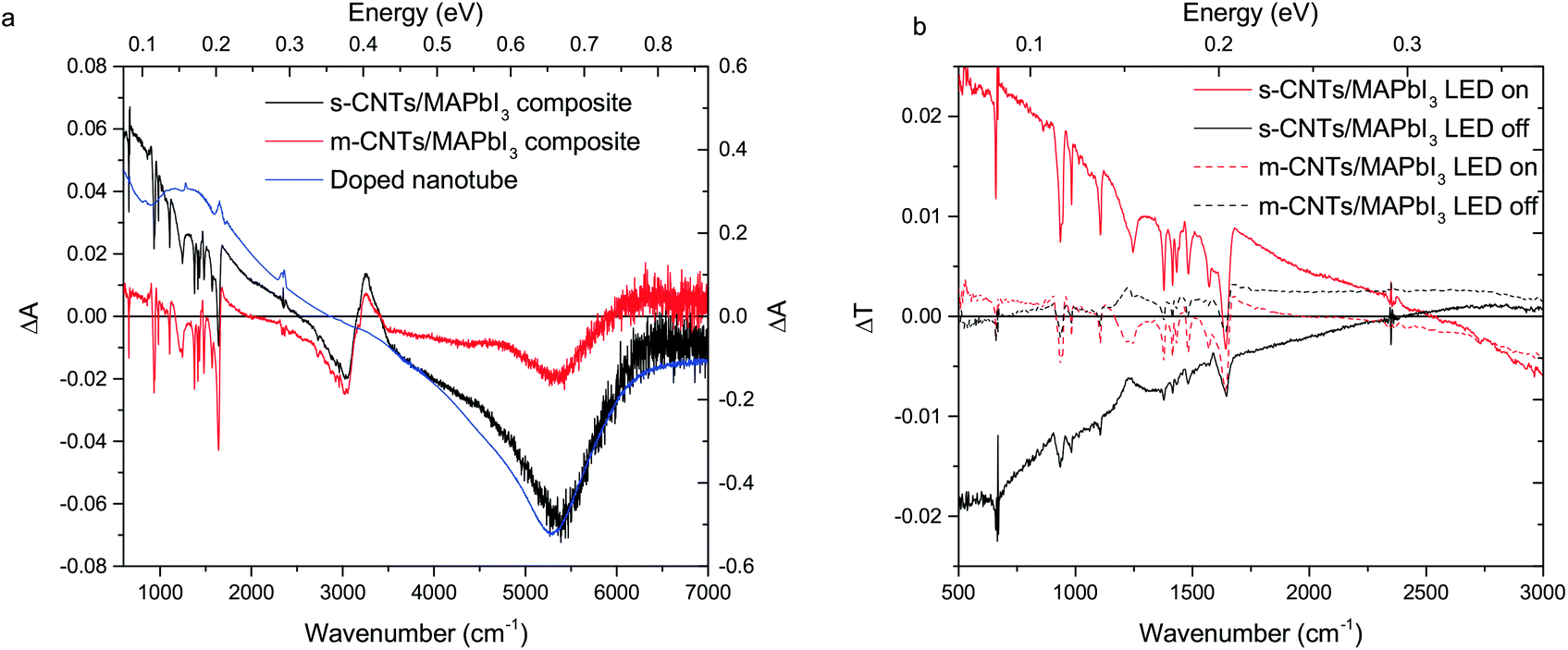 | ||
| Fig. 4 (a) Comparison of the light-induced changes of semiconducting and metallic nanotube composite samples with chemically doped CNTs. (b) Comparison of the change in transmission (without normalization) in the case of semiconducting and metallic nanotube composite samples. Metallic nanotubes show negligible change compared to the semiconducting tubes upon turning the light on or off. | ||
The main features in the difference spectra of the composite samples are related to the nanotubes. Carbon nanotubes are sensitive to their environment: coming in contact with other materials usually results in charge transfer to some extent. The direction and amount of electrons transferred depends on the electronic structure of both materials. Since pristine nanotubes show no photoresponse, the observed changes must originate in the different amounts of charge transfer from MAPbI3 in the case of measurements under dark/illuminated conditions.
We can consider the composite sample as a semiconductor heterojunction (Fig. 5) similar to what was suggested by Schulz et al.21 By forming a contact between the CNTs and MAPbI3 the bands shift in order to align the Fermi levels. The conduction and valence bands bend to compensate for the different energy levels on the two sides of the junction. The band bending is a result of electron transfer from one side to the other. While MAPbI3 behaves like a bulk semiconductor where the band far from the junction is unaffected, in the nanotube the band shifting is extended throughout the whole length of the tube due to the unscreened Coulomb interaction resulting from the one dimensional nature of the nanotube.35 Thus, instead of bending, the bands of the nanotube are shifted similar to gating or chemical doping. The main difference between the two types of heterojunctions is that while in the semiconducting case the charge transfer affects the highest occupied Van Hove singularity creating a high density of states at the Fermi level (Fig. 5b), in the metallic case the shift does not change the number of states due to the energy independent density of states of the metallic nanotubes (Fig. 5e). The amount of charge transfer depends on the electronic properties in the same way as the band gap of the materials. The charge transfer between the two materials can be directly observed by electrical transport measurements as well (ESI, Fig. S4†). To elucidate the origin of the observed light-induced changes we investigated the time dependence with a series of illuminated and dark measurements.
 | ||
| Fig. 5 (a) Energy band of MAPbI3 and an s-CNT before forming the contact. (b) Band alignment in s-CNTs/MAPbI3 heterojunction in the dark (the band of the MAPbI3 bends to compensate for the energy level differences); and (c) after illumination. (d) Energy band of MAPbI3 and an m-CNT before forming the contact. (e) Band alignment in the m-CNT/MAPbI3 heterojunction in the dark; and (f) after illumination. | ||
Fig. 6 shows the time dependence of the difference spectrum in the free carrier region for the s-CNT/MAPbI3 composite. It consists of a rapid component in the variation of the optical density and a slow one, which extends to a timescale of tens of minutes in the case of illumination. When the light is switched off, after the initial faster decrease it takes more than an hour to relax back to the original dark state.
 | ||
| Fig. 6 Time dependence of the light-induced changes in the free-carrier response region (550 cm−1). After an initial fast response, it shows a slow response both in the “on” and “off” states extending to tens of minutes. | ||
The change in optical absorption arises from the diffusion of the photo-excited electrons through the interface into the carbon nanotubes. Even a small number of photoelectrons (of the order of 1015 cm−3) can produce a noticeable change because they occupy the first excited Van Hove singularity with high density of states. As this process results in a partially filled band, the number of free carriers increases, resulting in low-frequency absorption. At the same time, as there are less available final states for the S11 optical excitation within the CNTs, the absorption around 5300 cm−1 decreases. The slow change of the optical density has a different origin. Similar, extremely slow variations have been observed in this family of materials23–25 and ascribed to the decrease of the organic cation binding energy due to illumination. The organic cations in this less bound state can distort the metal halide cage. It is known that the band gap of the organo-halide perovskites depends on the metal–halide–metal bond angle and distance. The light-induced weakening of the bonds between the organic cation and the metal halide cage in turn changes slightly the band gap of the material. Under this new condition the adjustment of the Fermi levels induces a carrier flow through the interface to establish the new charge balance. This change, as reported in ref. 24, is reversible on a similar timescale as observed here. This simplified picture is also consistent with the response obtained for the m-CNT/MAPbI3 composite. All the changes in the charge flow happen at EF, at the very low density of states region of the carbon nanotubes that does not produce measurable changes in the optical density. This does not mean that there is no charge flow towards the metallic CNTs; however, this charge flow does not produce enough free carriers to influence the photocurrent significantly. In other words, for efficient free carrier extraction one needs to use s-CNTs, that have been the choice in previous studies.9,21,22
4. Conclusions
The simultaneous and opposite change in the S11 and Drude peak and the absence of increase in the D band intensity in the Raman spectra of the CNT/MAPbI3 composites narrows down the explanation of the observed changes to charge transfer between the two materials upon visible light illumination. We found that the time dependence of the nanotube optical features follows that of free standing MAPbI3 films, showing a fast and a slow component. We have identified a fast component that is very likely to come from the photoexcited carriers in the MAPbI3. This response is important in CNT/MAPbI3 composite detectors and sensors, where a fast response is required and the signal is amplified by the peculiar band structure of the CNTs.15 The charge transfer by the slow component in the optical response, ascribed to the structural, bond-angle relaxation upon illumination, followed by Fermi level alignment is useful in solar cell applications. In this case the fast response is not a requirement since the material is exposed to constant illumination in time. Nevertheless, it is likely that for both components, fast and slow, the quality of the interface plays a role, whose optimization should be addressed in the future in order to reduce the trap density.Conflicts of interest
There are no conflicts to declare.Acknowledgements
Work in Budapest was supported by the Hungarian National Research Fund (OTKA) through grant no. NK 105691 and by the European Structural and Investment Funds jointly financed by the European Commission and the Hungarian Government through grant no. VEKOP-2.3.2-16-2016-00011 and VEKOP-2.3.3-15-2016-00001. Á. P. gratefully acknowledges support from the János Bolyai Fellowship of the Hungarian Academy of Sciences and from the National Research, Development and Innovation Office – NKFIH PD 121320. Special thanks are due to Zoltán Dankházi at the SEM Laboratory, Research and Instrument Core Facility (RICF), Faculty of Science, Eötvös University, Budapest. In Lausanne the research was financed by the Swiss National Science Foundation and by the ERC Advanced Grant Picoprop (670918).References
- H.-S. Kim, C.-R. Lee, J.-H. Im, K.-B. Lee, T. Moehl, A. Marchioro, S.-J. Moon, R. Humphry-Baker, J.-H. Yum, J. E. Moser, M. Grätzel and N.-G. Park, Sci. Rep., 2012, 2, 591 CrossRef PubMed.
- G. Xing, N. Mathews, S. Sun, S. S. Lim, Y. M. Lam, M. Grätzel, S. Mhaisalkar and T. C. Sum, Science, 2013, 342, 344–347 CrossRef CAS PubMed.
- M. A. Green, A. Ho-Baillie and H. J. Snaith, Nat. Photonics, 2014, 8, 506–514 CrossRef CAS.
- X. Mettan, R. Pisoni, P. Matus, A. Pisoni, J. Jaćimović, B. Náfrádi, M. Spina, D. Pavuna, L. Forró and E. Horváth, J. Phys. Chem. C, 2015, 119, 11506–11510 CAS.
- A. Pisoni, J. Jaćimović, O. S. Barišić, M. Spina, R. Gaál, L. Forró and E. Horváth, J. Phys. Chem. Lett., 2014, 5, 2488–2492 CrossRef CAS PubMed.
- M. Saliba, T. Matsui, J. Y. Seo, K. Domanski, J. P. Correa-Baena, M. K. Nazeeruddin, S. M. Zakeeruddin, W. Tress, A. Abate, A. Hagfeldt and M. Grätzel, Energy Environ. Sci., 2016, 9, 1989–1997 CAS.
- Research Cell Efficiency Records; http://www.Nrel.Gov/Ncpv/Images/Efficiency_Chart.jpg (accessed: February 2016).
- U. Bach, D. Lupo, P. Comte, J. E. Moser, F. Weissortel, J. Salbeck, H. Spreitzer and M. Grätzel, Nature, 1998, 395, 583–585 CrossRef CAS.
- S. N. Habisreutinger, T. Leijtens, G. E. Eperon, S. D. Stranks, R. J. Nicholas and H. J. Snaith, J. Phys. Chem. Lett., 2014, 5, 4207–4212 CrossRef CAS PubMed.
- S. N. Habisreutinger, T. Leijtens, G. E. Eperon, S. D. Stranks, R. J. Nicholas and H. J. Snaith, Nano Lett., 2014, 14, 5561–5568 CrossRef CAS PubMed.
- K. Aitola, K. Sveinbjornsson, J. P. Correa-Baena, A. Kaskela, A. Abate, Y. Tian, E. M. J. Johansson, M. Grätzel, A. Hagfeldt and G. Boschloo, Energy Environ. Sci., 2016, 9, 461–466 CAS.
- Z. Li, S. A. Kulkarni, P. P. Boix, E. Shi, A. Cao, K. Fu, S. K. Batabyal, J. Zhang, Q. Xiong, L. H. Wong, N. Mathews and S. G. Mhaisalkar, ACS Nano, 2014, 7, 6797–6804 CrossRef PubMed.
- F. J. Wang, M. Endo, S. Mouri, Y. Miyauchi, Y. Ohno, A. Wakamiya, Y. Murata and K. Matsuda, Nanoscale, 2016, 8, 11882–11888 RSC.
- M. Spina, M. Lehmann, B. Náfrádi, L. Bernard, E. Bonvin, R. Gaál, A. Magrez, L. Forró and E. Horváth, Small, 2015, 11, 4824–4828 CrossRef CAS PubMed.
- M. Spina, B. Náfrádi, H. M. Tóháti, K. Kamarás, R. Gaál, L. Forró and E. Horváth, Nanoscale, 2016, 8, 4888–4893 RSC.
- L. J. Yang, S. Wang, Q. S. Zeng, Z. Y. Zhang and L. M. Peng, Small, 2013, 9, 1225–1236 CrossRef CAS PubMed.
- J. Y. Jeng, Y. F. Chiang, M. H. Lee, S. R. Peng, T. F. Guo, P. Chen and T. C. Wen, Adv. Mater., 2013, 25, 3727–3732 CrossRef CAS PubMed.
- Y. H. Shao, Z. G. Xiao, C. Bi, Y. B. Yuan and J. S. Huang, Nat. Commun., 2014, 5, 5784 CrossRef CAS PubMed.
- T. Chen, L. B. Qiu, Z. B. Cai, F. Gong, Z. B. Yang, Z. S. Wang and H. S. Peng, Nano Lett., 2012, 12, 2568–2572 CrossRef CAS PubMed.
- X. Y. Xia, S. S. Wang, Y. Jia, Z. Q. Bian, D. H. Wu, L. H. Zhang, A. Y. Cao and C. H. Huang, J. Mater. Chem., 2010, 20, 8478–8482 RSC.
- P. Schulz, A.-M. Dowgiallo, M. Yang, K. Zhu, J. L. Blackburn and J. J. Berry, J. Phys. Chem. Lett., 2016, 7, 418–425 CrossRef CAS PubMed.
- R. Ihly, A.-M. Dowgiallo, M. Yang, P. Schulz, N. J. Stanton, O. G. Reid, A. J. Ferguson, K. Zhu, J. J. Berry and J. L. Blackburn, Energy Environ. Sci., 2016, 9, 1439–1449 CAS.
- R. Gottesman, E. Haltzi, L. Gouda, S. Tirosh, Y. Bouhadana, A. Zaban, E. Mosconi and F. De Angelis, J. Phys. Chem. Lett., 2014, 5, 2662–2669 CrossRef CAS PubMed.
- R. Gottesman, L. Gouda, B. S. Kalanoor, E. Haltzi, S. Tirosh, E. Rosh-Hodesh, Y. Tischler, A. Zaban, C. Quarti, E. Mosconi and F. De Angelis, J. Phys. Chem. Lett., 2015, 6, 2332–2338 CrossRef CAS PubMed.
- R. Gottesman and A. Zaban, Acc. Chem. Res., 2016, 49, 320–329 CrossRef CAS PubMed.
- A. A. Green and M. C. Hersam, Nano Lett., 2008, 8, 1417 CrossRef CAS PubMed.
- Z. C. Wu, Z. H. Chen, X. Du, J. M. Logan, J. Sippel, M. Nikolou, K. Kamaras, J. R. Reynolds, D. B. Tanner, A. F. Hebard and A. G. Rinzler, Science, 2004, 305, 1273–1276 CrossRef CAS PubMed.
- A. Poglitsch and D. Weber, J. Chem. Phys., 1987, 87, 6373–6378 CrossRef CAS.
- E. Horváth, M. Spina, Z. Szekrényes, K. Kamarás, R. Gaal, D. Gachet and L. Forró, Nano Lett., 2014, 14, 6761–6766 CrossRef PubMed.
- I. Ka, L. F. Gerlein, R. Nechache and S. G. Cloutier, Sci. Rep., 2017, 7, 45543 CrossRef CAS PubMed.
- T. Baikie, Y. Fang, J. M. Kadro, M. Schreyer, F. Wei, S. G. Mhaisalkar, M. Grätzel and T. J. White, J. Mater. Chem. A, 2013, 1, 5628–5641 CAS.
- N. Onoda-Yamamuro, T. Matsuo and H. Suga, J. Phys. Chem. Solids, 1990, 51, 1383–1395 CrossRef CAS.
- Á. Pekker and K. Kamarás, Phys. Rev. B: Condens. Matter, 2011, 84, 075475 CrossRef.
- F. Borondics, K. Kamarás, M. Nikolou, D. B. Tanner, Z. Chen and A. G. Rinzler, Phys. Rev. B: Condens. Matter, 2006, 74, 045431 CrossRef.
- F. Léonard and J. Tersoff, Phys. Rev. Lett., 1999, 83, 5174–5177 CrossRef.
Footnote |
| † Electronic supplementary information (ESI) available. See DOI: 10.1039/C7NR06136F |
| This journal is © The Royal Society of Chemistry 2017 |