
 Open Access Article
 This Open Access Article is licensed under a
 Creative Commons Attribution 3.0 Unported Licence
Zero-dimensional methylammonium iodo bismuthate solar cells and synergistic interactions with silicon nanocrystals†
Calum
McDonald
 *a,
Chengsheng
Ni
b,
Vladimir
Švrček
c,
Mickaël
Lozac'h
c,
Paul A.
Connor
b,
Paul
Maguire
a,
John T. S.
Irvine
b and
Davide
Mariotti
a
*a,
Chengsheng
Ni
b,
Vladimir
Švrček
c,
Mickaël
Lozac'h
c,
Paul A.
Connor
b,
Paul
Maguire
a,
John T. S.
Irvine
b and
Davide
Mariotti
a
aNanotechnology and Integrated Bioengineering Centre, Ulster University, BT37 0QB, UK. E-mail: mcdonald-c26@email.ulster.ac.uk
bSchool of Chemistry, University of St Andrews, KY16 9ST, UK
cResearch Center for Photovoltaics, National Institute of Advanced Industrial Science and Technology (AIST), Tsukuba 305-8568, Japan
First published on 23rd November 2017
Abstract
Organometal trihalide perovskite solar cells have attracted monumental attention in recent years. Today's best devices, based on a three-dimensional perovskite structure of corner-sharing PbI6 octahedra, are unstable, toxic, and display hysteresis in current–voltage measurements. We present zero-dimensional organic–inorganic hybrid solar cells based on methylammonium iodo bismuthate (CH3NH3)3(Bi2I9) (MABI) comprising a Bi2I9 bioctahedra and observe very low hysteresis for scan rates in the broad range of 150 mV s−1 to 1500 mV s−1 without any interfacial layer engineering. We confirm good stability for devices produced and stored in open air without humidity control. The MABI structure can also accommodate silicon nanocrystals, leading to an enhancement in the short-circuit current. Through the material MABI, we demonstrate a promising alternative to the organometal trihalide perovskite class and present a model material for future composite third-generation photovoltaics.
1. Introduction
Organometal trihalide perovskites (OTPs) have attracted significant interest after their first report in a photovoltaic cell in 20091 and record power conversion efficiency (PCE) now exceeding 22%.2 OTPs are attractive particularly due to their ease of processing,3,4 large absorption coefficient,5 long carrier diffusion lengths,6,7 low exciton binding energy,8 and low non-radiative recombination rates.9 OTPs are of the form ABX3, where A is a monovalent cation (e.g. methylammonium (MA) CH3NH3, formamidinium (FA) CH3(NH2)2), B is a divalent metal cation (e.g. Pb2+, Sn2+) and X is an anion (e.g. I−, Cl−, Br−, SCN−). Perovskites of mixed cations and/or anions are now typical for high efficiency cells.10–13 Although exceptional PCEs have been demonstrated by Pb-containing OTPs, the intention to solve the issues concerning low stability, toxicity, and rate-dependent current–voltage hysteresis is dominating current research efforts. OTPs are highly susceptible to degradation via deprotonation of the organic component which is driven by, for the most part, the presence of water moisture, oxygen, and trapped charges.14 The decomposition of Pb-containing OTPs leads to the formation of highly water-soluble Pb-halide compounds which presents a significant ecological issue.15The extreme susceptibility of OTPs to moisture requires critical control of the atmosphere during fabrication and entire device encapsulation in glass to prevent exposure to moisture and mechanical fractures. These measures may eliminate the possibility of flexible, low-weight modules and necessitates careful recycling. Even so, degradation is still observed in encapsulated devices16 and even for devices stored in vacuum.17,18 Mobile ions at the perovskite surface can diffuse through organic transport layers leading to degradation.19 Furthermore, noble metals have also been demonstrated to migrate through the organic hole transport material (HTM) to the OTP causing shunts across the device and also creating deep trap states reducing device performance.20 The first measure to improve the stability of OTP devices requires the replacement of the organic HTM with a more stable inorganic material.20,21 In spite of this, defects present in the OTP structure can facilitate vacancy migration,22 cause charge accumulation,23 phase segregation,24 and lattice distortions and strain in the perovskite structure,23,25,26 which have been suggested to impact negatively on stability.14,27 Improving crystal quality should lead to improved stability;14,28 however, the fabrication of high-purity, defect-free OTPs is challenging and may preclude the realization of low-cost OTP solar cell devices, whilst the extent to which the stability can be improved is unknown and the outlook for long-term stability remains unclear.
High stability may be realised through an all-inorganic device, yet the best inorganic perovskite device to date, CsPbBr3 with ∼6% PCE,29 is lead-containing, unstable, and tends to exhibit significant current–voltage hysteresis.30–32 The contamination of Pb in OTPs can be addressed either by replacing Pb with other non-toxic elements or by stabilising the structure of the perovskite to avoid the formation of PbI2. Lead-free OTPs have been produced by direct replacement of Pb with Sn33–35 with 6% PCE.34 However, poor stability is observed in tin-based devices due to the tendency of tin to oxidise easily from Sn2+ to Sn4+. This has been addressed to some extent by the addition of SnF2 which acts as an inhibitor for Sn4+ formation, but a reduction in the PCE was observed.36 Moreover, computational studies suggest that there is no replacement for Pb in OTPs to achieve similarly high PCEs, and the best avenue for bulk OTPs should be composites of Pb and Mg serving only to reduce the Pb content.37 Alternatively, reducing the dimensionality of OTPs can improve the stability, such as forming two-dimensional layered perovskites.38 Low-dimensional networks of metal halides stabilised by organic cations are emerging as a promising route towards solving the stability issues of current OTPs.38–40
The hysteresis observed in OTPs is mostly attributed to ion migration and charge accumulation in the OTP.41–44 Hysteresis is problematic as it primarily introduces difficulties in accurately measuring device performance, but also indicates low stability.27 Selecting appropriate contacts and interface engineering can negate most of the hysteresis observed during standard device measurement.45–47 Despite this, the issues pertaining to defect migration and charge accumulation described remain, which can result in degradation of the OTP.14 Recent work11,13 has shown that current state-of-the-art mesoscopic devices possess low hysteresis in the forward and backward current density–voltage (J–V) scans with the same scan rates from 10 mV s−1 to 50 mV s−1. Hysteresis in OTPs is still well observed particularly for fast scans.21,43,48 In addition, it is typical that when carrying out hysteresis studies on OTPs, only a small range of scan rates are reported, generally 10–200 mV s−1.11,21,49
OTPs are also particularly temperature sensitive.50 MAPbI3, for example, exhibits a grain-size dependent phase transition typically observed around 330 K,4,51 which is within the operating temperature range of solar cells and introduces challenges in accurately determining the performance and stability of OTP solar cells. Low-cost and long-term stability should be realised through air-stable low-temperature solution-processable materials, possibly via reducing structural dimensionality, with phase-stability across the operating temperature regime, and hysteresis-less behaviour over a broad range of scan rates prior to interfacial layer engineering.
The lead free organic–inorganic hybrid material methylammonium iodo bismuthate, MA3Bi2I9, (herein MABI), unlike OTPs such as MAPbX3, is a zero-dimensional organic–inorganic hybrid material comprised of clusters of Bi2I9 bioctahedra separated spatially by approximately 0.16 nm and surrounded by methylammonium cations.52 This specific ordered arrangement with spatially confined clusters suggests the possibility of exploiting carrier multiplication, either through multiple exciton generation (MEG) or through space-separated quantum cutting (SSQC). MEG is normally considered to occur within single quantum confined nanocrystals (NCs)53–56 while SSQC occurs via photon absorption in one NC producing an excited carrier which can then interact with the valence electron of an adjacent NC such that the carrier multiplication occurs in the spatially separated NCs57 (or quantum confined clusters). We recently observed the effect of SSQC in MABI and reported evidence for carrier multiplication through the observation of an increased photoluminescence quantum yield (PLQY) onset at roughly twice the bandgap.58 Due to the close spacing of Bi2I9 clusters it is possible that SSQC can take place between adjacent Bi2I9 clusters.
MABI thin films have demonstrated superior air stability to MAPbI3 and is far less susceptible to moisture.59,60 Direct comparison of MABI with MAPbI3 in ambient conditions over 26 days revealed that MABI possess a more stable XRD spectra with a slight colour change after 26 days. Conversely, a complete colour change was observed for MAPbI3 after 13 days (from brown to yellow), signifying the formation of PbI2, confirmed by the emergence of a PbI2 peak in the XRD spectrum after 13 days which continued to increase in intensity. MABI has also demonstrated good stability when stored in ambient conditions with relative humidity Hr = 55% ± 5%.60 Hoye et al. attributed the improved stability of MABI to the formation of a stable surface layer of either Bi2O3 or BiOI which does not increase the surface recombination rate.59 In addition, no phase transformation is observed between −50 °C to 140 °C in differential scanning calorimetry58 indicating that MABI is more stable than MAPbI3 in the device operating temperature regime.
MABI solar cells have been reported with PCEs 0.42%60 using spiro-MeOTAD and mesoporous-TiO2 through careful optimization of the MABI layer. These devices were prepared in a glovebox and the stability of the devices was not reported, whilst there has not yet been a report on the hysteresis at varying scan rates for leading devices in the literature. It is estimated that the PCE of MABI devices can rise to 8% with short-circuit current density (JSC) as high as 10 mA cm−2 based on an open circuit voltage (VOC) of 1 V through optimization of the crystallization of MABI and interfacial quality.61 The improvement in the PCE of MABI devices has been slow compared to the meteoric rise in the efficiency of OTPs. The low PCE can largely be attributed to the low JSC, typically 0.5 mA cm−2 to 1 mA cm−2 for the best performing devices.60–63 High-performing MABI devices can be achieved by optimised film formation and stoichiometry, and careful control of interfaces with transport layers to supress recombination. However, the performance of MABI devices is hindered by its large bandgap reported as approximately 2.1 eV,59,62–64 high effective masses for carries,65 and high exciton binding energy64,65 which therefore results in inefficient exciton splitting and carrier extraction. MABI has also been shown to possess anisotropic charge mobility, with higher mobility in the a–b plane than in the c-axis.65 As well as optimising film formation, methods to reduce the exciton binding energy and increase carrier mobility should also be explored.
Overall, MABI is an environmentally friendly material, without the presence of Pb, and possesses unique material characteristics that offer a model architecture to explore new avenues for perovskite photovoltaics and with great potential for third-generation solar cell developments. We report here stable and hysteresis-less solar cell devices even when fabricated and stored in open-air conditions and without modification of the HTM or interfacial layers, and demonstrate MABI as a model material for third-generation photovoltaics. We demonstrate hysteresis-free devices due to the spatially separated Bi2I9 bioctahedral structure compared to the PbI6 octahedral framework and study the device stability with different metal contacts. In addition to this, we incorporate silicon nanocrystals (SiNCs) into the MABI matrix and observe that the structure can favourably accommodate SiNCs whilst exploring the interplay between Bi2I9 clusters and SiNCs, both within the respective quantum confined regimes and highlighting the potential for exciton handling. We therefore demonstrate an enhancement in JSC through the incorporation of SiNCs which may assist in the dissociation of excitons on MABI clusters. These results and exciton handling by SiNCs suggest opportunities to design new zero-dimensional hybrid materials for the utilization of carrier multiplication and the fabrication of third-generation devices.
2. Experimental details
2.1 MABI layer formation
MABi2I9 films were formed by first preparing a solution of BiI3 (1.65 M) and CH3NH3I (2.475 M) in dimethylformamide (DMF) solvent. The solution was stirred for 10 minutes at 80 °C and then spin-coated (1250 RPM for 20 s). The films were then annealed on a hot plate at 100 °C for 30 min2.2 Silicon nanocrystal (SiNC) synthesis
SiNCs were produced by the electrochemical etching of p-type Si-wafer (HF![[thin space (1/6-em)]](https://www.rsc.org/images/entities/char_2009.gif) :ethanol 1:4, constant current 20 mA cm−2) for 1 h.66–68 The powder was then mechanically removed and collected in a vial.
:ethanol 1:4, constant current 20 mA cm−2) for 1 h.66–68 The powder was then mechanically removed and collected in a vial.
2.3 Fabrication of solar cell devices
ITO-patterned glass substrates were cleaned by O2 plasma using a Diener Electronic Femto type E plasma system for 40 min. The TiO2 compact blocking layer was formed by dissolving 1.56 mL titanium(IV) isopropoxide and 0.35 mL triethanolamine in 18 mL ethanol, stirred for 2 hours at 40 °C and then left for 24 h. The solution was spin-coated, 5000 revolution per minute (RPM) for 30 s, and then annealed at 400 °C in a furnace for 2 h. The mesoporous TiO2 layer was deposited by spin-coating (2000 RPM for 60 s) from a solution of commercial Dyesol 18-NRT titania nanoparticle paste and ethanol in a 1:2 ratio of paste to ethanol. The films were then annealed again in a furnace at 400 °C for 2 h. The MABI layer was then deposited by spin coating as described above.
In order to defragment the SiNCs from large agglomerates and enhance the interaction with MABI, SiNCs were treated directly in DMF with fs-laser irradiation following a similar method reported previously.69 5 mg of SiNCs were suspended in 3 mL dimethylformamide (DMF). The fs-laser process used a wavelength of 400 nm and pulse width of 100 fs. Barium Borate (BBO) crystal was used to select 400 nm. The process was conducted at room temperature and for 30 min. The laser beam was shaped and focused onto a spot (2 mm in diameter) on the liquid surface by an optical lens with a focal length of 250 mm. The average laser power was set to be approximately 30 mW while using the repetition of 1 kHz. During the irradiation, the glass container was rotated. Laser treatment was used both to induce the fragmentation and surface passivation of the SiNCs. BiI3 (1.65 M) and CH3NH3I (2.475 M) was then added to the DMF solution containing SiNCs and the solution was spin-coated according to the method previously described and annealed on a hot plate at 100 °C for 30 min. The content of SiNCs was approximately 0.1 wt%.
The hole transport layer was prepared by dissolving 0.207 g 2,2′,7,7′-tetrakis[N,N-di(4-methoxyphenyl)amino]-9,9′-spirobifluorene (Spiro-MeOTAD) in 1 mL chlorobenzene and deposited by spin-coating (1500 RPM for 20 s). Silver and gold metal contacts were deposited by thermal evaporation using a shadow mask. The resulting active area of the device was 0.04 cm2.
2.4 X-Ray diffraction (XRD)
XRD measurements were performed using a Bruker D8 Discover system, using Cu K-alpha X-rays with wavelength 1.54 Å. XRD measurements were performed on MABI films prepared by spin coating on quartz glass.2.5 Ultraviolet–visible absorption spectroscopy
Absorption measurements were carried out using a PerkinElmer Lambda 650 UV-vis spectrophotometer with a spectral range between 190 nm and 900 nm using tungsten–halogen and deuterium lamps, fitted with a 150 mm integrating sphere and performed by placing the substrate on the reflectance port of the integrating sphere. UV-Vis measurements were carried out on MABI films prepared by spin coating on quartz glass.2.6 X-Ray photoelectron spectroscopy (XPS)
XPS was performed using a Kratos Axis Ultra DLD photoelectron spectrometer with monochromatic Al K-alpha X-ray radiation. Current and voltage were 10 mA and 15 kV, respectively, at an operating pressure of 10−9 bar. MABI was deposited by spin coating onto molybdenum foil, and the binding energies were referenced to the Mo 3d peak (228 eV) from the molybdenum foil substrate.2.7 Scanning electron microscopy (SEM)
SEM images were collected using a JEOL JSM-6010LV. Samples were prepared on glass substrates with the structure glass/compact-TiO2/mesoporous-TiO2/MABI and glass/compact-TiO2/mesoporous-TiO2/MABI + SiNCs. For the fabrication of MABI + SiNC layers, 1.67 mg of the as-collected SiNCs were added to 1 mL of DMF. The solution was then ultrasonicated for 30 min. BiI3 (1.65 M) and CH3NH3I (2.475 M) was then added to the SiNCs in DMF solution and the solution was stirred on a hotplate for 10 min at 100 °C. The deposition was then carried out by spin coating and then annealing as previously described.2.8 Power conversion efficiency
Normalized solar spectrum AM1.5G was generated using Wacom Electric Co. solar simulator (JIS, IEC standard conforming, CLASS AAA) calibrated to give 100 mW cm−2 using an amorphous silicon (a-Si) reference cell. The electrical data was recorded using a Keithley 2400 source meter. Devices were measured in the voltage range −0.1 V to 0.6 V without any pre-conditioning (i.e. without voltage soaking or light soaking) and measured using scan rates between 150 mV s−1 and 1500 mV s−1. The scan rate was varied by altering the full J–V curve acquisition time, whilst each current point acquisition at a specific applied voltage remained constant for all measurements. This was achieved by altering the voltage step size and the number of points measured between a fixed voltage range, which ensures that each data point is measured under the same conditions. The number of power line cycles (NPLC), i.e. the number of times the input signal is integrated to obtain a single measurement, was set to 10 cycles and the delay time, i.e. the delay between applying the voltage and the measurement of the signal, was set to 5 ms. The NPLC and the delay time remained constant for all measurements.2.9 External quantum efficiency (EQE)
The solar cell EQE characteristics were measured in direct current (DC) mode using a Eko Seiki SPM-005B system with 150 W Xenon lamp and monochromator, and the spectral response was calibrated using an a-Si reference cell.3. Results and discussion
3.1 MABI characterization and properties
We have previously studied in detail the structure and composition of our MABI films.58 Single-crystal XRD has revealed hexagonal crystal structure with P63/mmc space group.52 We have used XRD to study the crystallinity of spin-coated MABI films. Fig. 1 shows the XRD pattern for MABI deposited on quartz glass by spin coating. The XRD pattern reveals that the MABI film is highly orientated in the [001] direction. Fig. S1† shows the X-ray photoelectron (XPS) spectra for MABI deposited on molybdenum foil by spin coating. The XPS measurement was performed the following day after film formation, and the results demonstrate that the surface of the MABI film is not degraded in ambient air.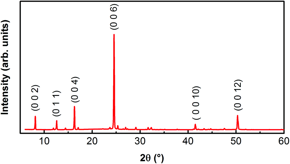 | ||
| Fig. 1 X-ray diffraction pattern for MABI layer deposited on quartz glass, showing that the film is highly orientated in the [001] direction. | ||
Fig. 2 shows the measured ultraviolet-visible (UV-vis) transmittance spectrum of MABI and the indirect and direct optical bandgaps have been determined using Tauc plots. The bandgap has been reported to vary between 1.96 eV and 2.26 eV.52,65 Density functional theory (DFT) predicted that MABI has an indirect gap of 1.97 eV and a direct gap of 2.17 eV,65 whilst Abulikemu et al. report that the bandgap varies due to the size and orientation of the MABI crystals.52 We therefore produced Tauc plots for both an indirect transition and a direct transition. For the indirect transition, the energy gap is determined as 1.99 eV (Fig. 2b) and for the direct transition the energy gap is determined as 2.15 eV (Fig. 2c). The indirect and direct transition values calculated from the Tauc plot are in very good agreement with those calculated using DFT,65 whilst we do not rule out that the bandgap may also vary due to size and orientation of the MABI crystals.
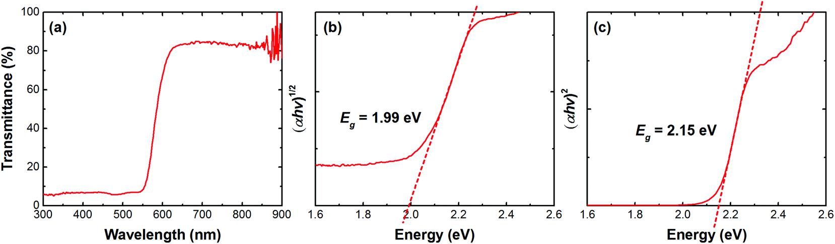 | ||
| Fig. 2 Transmittance and Tauc plots for MABI thin film on quartz. (a) Transmittance spectrum, (b) Tauc plot for indirect transition giving a bandgap (Eg) of 1.99 eV and (c) Tauc plot assuming a direct transition giving Eg of 2.15 eV. | ||
3.2 Solar cell device fabrication and characterization
We investigated the organic–inorganic hybrid material MABI (MA3Bi2I9) for solar cell applications. MABI can be solution-processed in a very similar manner to the organic–inorganic lead halide perovskites. We present devices with the structure indium tin–oxide (ITO)/compact-TiO2/mesoporous-TiO2/MABI/Spiro-MeOTAD/Au or Ag. All device fabrication and storage was carried out in open-air conditions. Solar cell devices were fabricated using MABI as the active layer and the J–V characteristic and external quantum efficiency (EQE) for the best performing solar cell are shown in Fig. 3a and b. Devices produced with Au contacts displayed higher efficiency than Ag contacts (ESI Fig. S2†), with highest recorded PCE of 0.164% for devices with Au shown in Fig. 3a. The lower performance of devices with Ag can be attributed to the less favourable work function which provides a smaller field in the hole transport layer, and also the rapid degradation of Ag into AgI (presented later). The JSC calculated from the EQE for the champion cell was 0.694 mA cm−2.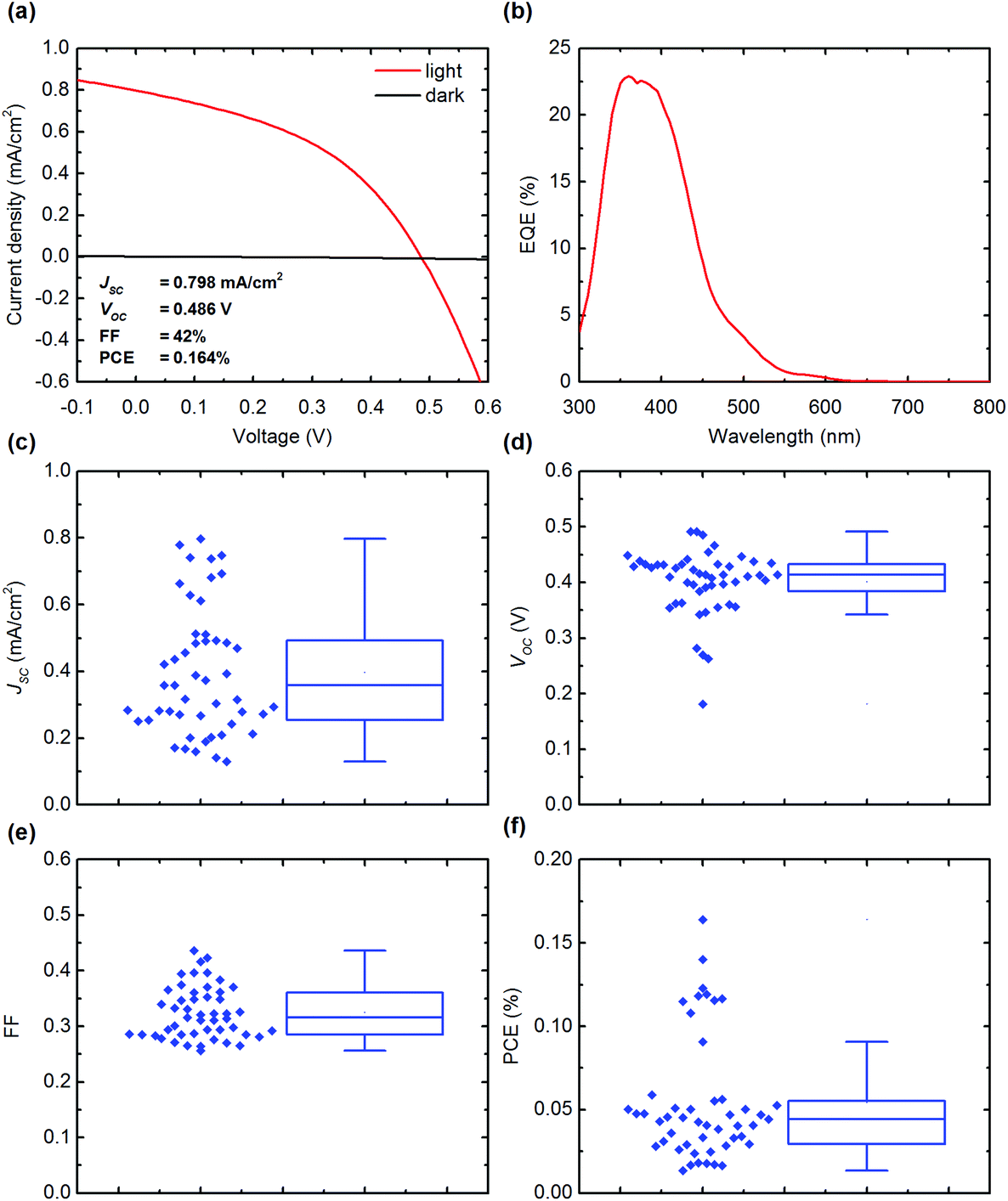 | ||
| Fig. 3 MABI solar cell device performance under normalized AM1.5G solar spectrum with irradiance of 100 mW cm−2. (a) Current density–voltage characteristic and (b) external quantum efficiency (EQE) of the champion device with corresponding short-circuit current density (JSC), open-circuit voltage (VOC), fill factor (FF) and power conversion efficiency (PCE). (c–f) Device performance for 41 solar cells. The data are represented as standard box and whisker plots for (c) JSC, (d) VOC, (e) FF, and (f) PCE. All devices shown were produced with Au contacts. | ||
To confirm that the photocurrent is produced by the MABI layer, devices were also fabricated without the MABI active layer with the structure ITO/compact-TiO2/mesoporous-TiO2/Spiro-MeOTAD/Au. The EQE for these devices is shown in the ESI (Fig. S3†), and confirmed there was no contribution from the spiro-MeOTAD or the TiO2 layers, and the photocurrent is generated solely by absorption in the MABI layer.
The performance statistics for 41 devices is shown in Fig. 3c–f and plotted as standard box and whisker plots as per the standard Tukey boxplot, where the “box” represents the respective quartiles below and above the median, and the “whiskers” represent the lowest (highest) datum within a range defined by the interquartile range multiplied by a factor of 1.5, relative to the lower (upper) quartile. The statistical distribution originates from the repeatability of the various device fabrication steps intrinsic to lab processes including variations in day-to-day humidity, also considering that all devices were prepared in open-air conditions.
The presence of hysteresis in MABI solar cells was then investigated. The J–V characteristics at varying scan rates and scan directions is shown in Fig. 4a and b. The J–V characteristic for a scan rate of 150 mV s−1 in the forward and backward direction is shown in Fig. 4a, and in Fig. 4b reports on different scan rates. The device shows very low hysteresis for both slow scans and fast scans. The low hysteresis observed when comparing the slow scans (150 mV s−1) with the very fast scans (1500 mV s−1) is a highly promising result, given that such a large range in the scan rate usually produces substantial hysteresis for the Pb-based organometal trihalide perovskite family when deposited on mesoporous-TiO2. This is an encouraging result for a mesoscopic solar cell considering that the interfacial layers are unmodified. In previous reports, Park et al. measured MABI devices with a scan rate of 100 mV s−1 and 800 mV s−1 and low hysteresis was observed. Lyu et al. also observed low hysteresis for a fixed scan rate, though the scan rate used was not specified. Recent reports have not further studied the hysteresis in MABI for varying scan rates.60,61
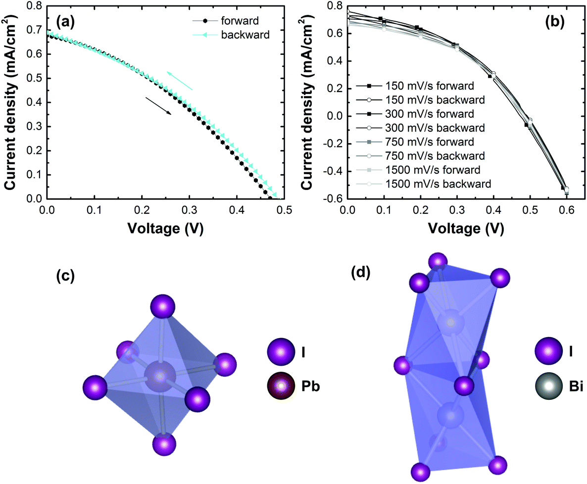 | ||
| Fig. 4 Hysteresis study for MABI solar cells indicating hysteresis-less behaviour. (a) Current density–voltage (J–V) characteristic measured in the forward and backward scan direction for a scan rate of 150 mV s−1 (0.01 V step size, 71 points), which is a typical scan rate selected for measuring conventional organometal trihalide perovskite solar cells. (b) J–V characteristic measured in the forward and backward scan direction for varying scan rates between 150 mV s−1 (0.01 V step size, 71 points) and 1500 mV s−1 (0.1 V step size, 8 data points). Some of the data points have been removed from (b) for clarity. (c) Octahedra adopted by PbI6 and (d) face-sharing bioctahedron adopted by Bi2I9. All J–V measurements were carried out in the voltage range −0.1 V to 0.6 V. | ||
In MAPbI3, hysteresis arises due to a number of reasons, and is mostly the result of combined ion migration and charge trapping at interfaces and grain boundaries.44 The hysteresis due to surface traps can be mostly diminished by surface passivation.47 The migration of ions in MAPbI3 causes a band bending in the cell due to the accumulation of positively and negatively charge defects at interfaces and grain boundaries.70 These defects can also facilitate trap-assisted recombination.44 The migration of iodine vacancies in MAPbI3 occurs easily along the lead iodide structure, and the connected network of PbI6 octahedra in all three axes accommodates the facile migration of iodine vacancies along the structure.71Fig. 4c shows the PbI6 octahedra, which is connected to adjected octahedral in every axial direction. This connectivity is broken in MABI, where the Bi2I9 bioctahedra (Fig. 4d) is disconnected in all three dimensions and is isolated by MA ions. The low hysteresis observed in MABI is likely due to the structure adopted by MABI, forming a zero-dimensional network of spatially separated face-sharing Bi2I9 bioctahedra surrounded by CH3NH3+ barriers. The absence of a connected lattice for iodine vacancies to migrate could inhibit ion migration of iodine between Bi2I9 bioctahedra. Furthermore, MABI is expected to form a native surface layer of Bi2O3 or BiOI which does not increase the recombination rate.59 The presence of the Bi2O3/BiOI surface layer could provide self-passivation against charge trapping at interfaces.
Furthermore, we investigated the stability of devices fabricated in open-air conditions, and then stored over a 21-day period in open-air and in the dark. Fig. 5a shows the stability of MABI devices produced with Ag and Au contacts. Devices produced with Au possessed the highest stability, with a small drop in efficiency over 21 days. The small reduction in PCE observed over 3 weeks is likely due to the fabrication in open-air conditions and thus the presence of moisture in the device, combined with the degradation of the spiro-MeOTAD layer. Nonetheless, MABI shows exceptional tolerance to moisture with respect to OTPs.
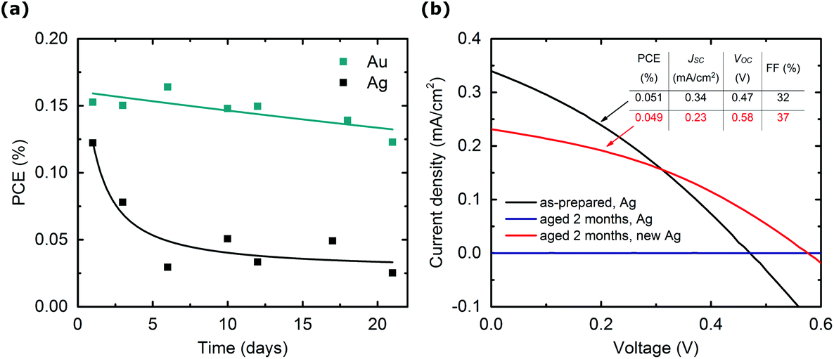 | ||
| Fig. 5 MABI solar cell stability. (a) Stability of MABI devices produced with silver and gold top contacts plotted as power conversion efficiency (PCE) with time and (b) current density–voltage curves for MABI solar cells with Ag under illumination, which demonstrates the high stability of the MABI layer after 2 months when the Ag contacts were replaced. The solar cell characteristics in (b) refers to as-prepared MABI devices fabricated with silver contacts (black line), after 2 months of aging in ambient conditions (blue line), and then with fresh silver contacts deposited on the same device (red line). This confirms that it is not the degradation of the MABI layer that leads to a reduction in the efficiency, rather the degradation due to the silver contacts. All devices shown in (a) and (b) were stored in ambient conditions in the dark. The scan rate that was used for all measurements was 150 mV s−1 and in the backward scan direction. | ||
For devices produced with Ag we observed low stability, with a severe degradation in efficiency after only 3 days due to the visible degradation of the Ag top contacts (Fig. 5, and individual J–V curves are shown in ESI Fig. S4† for Ag devices). Hoye et al. and Lyu et al. both observed high stability in the XRD patterns for MABI films deposited on quartz and FTO substrates respectively,59,62 indicating that the MABI material is independently stable, which Hoye et al. proposed is due to the formation of a surface layer of either Bi2O3 or BiOI.59 The degradation of Ag contacts is not observed for devices without the presence of MABI active layer, e.g. ITO/compact-TiO2/mesoporous-TiO2/Spiro-MeOTAD/Ag confirming that the presence of MABI is required to induce the degradation of Ag. In addition, when fresh Ag contacts are deposited on MABI devices 2 months after fabrication, the efficiency is comparable to that of the as-prepared devices (Fig. 5b). Devices produced with fresh contacts after 2 months displayed a reduction in JSC; however, there was a 0.11 V increase in VOC, possibly due to the evolution of the native surface layer.59
The formation of AgI on MAPbI3 solar cells with Ag contacts is well-reported and it is attributed to the decomposition of MAPbI3 into volatile species (I− and MA+). These species then migrate through the HTM and accumulate at the Ag electrode and react with Ag to form AgI.19,72 Previously, Park et al. reported good stability for MABI devices produced with Ag contacts fabricated and stored in a N2 glove box,63 which we expect is due to a thicker and more continuous layer of spiro-MeOTAD with reduced pinholes. Additionally, the fabrication in N2 glove box will reduce the presence of moisture at the MABI and Spiro-MeOTAD interface immediately after device fabrication, and therefore I− and MA+ defects are less prevalent. Although MABI displays a high tolerance to moisture individually, defects may exist at the surface such as I− and MA+ which are enhanced by the fabrication in open-air. If I− and MA+ defects are present at the surface, these can easily migrate through the HTM and decompose the Ag and account for the AgI formation. The migration of metal through spiro-MeOTAD has also been reported by Domanski et al. and was induced at temperatures as low as 75 °C after 15 hours.20 They confirmed that this irreversible degradation was not due to the decomposition of the organic and hybrid perovskite layers, and report that a Cr interlayer reduces the metal migration. Because we have stored devices at room temperature and in the dark between measurements, it is not expected that Ag is migrating significantly. The degradation of Ag due to I− and MA+ ions can likely be overcome by reducing the pinholes in the spiro-MeOTAD layer and/or by implementing an interlayer. The best MABI solar cell reported in the literature employed a MoO3 interlayer between spiro-MeOTAD and Ag, however the stability of a fabricated device was not reported.60 We can therefore confirm that MABI devices are highly stable when a suitable/stable contact interface is employed (e.g. with Au). The degradation of the device performance with Ag contacts is due to specific chemical reactions with Ag which are not due to MABI stability in general.
We have then explored the potential of MABI to form zero-dimensional hybrids by the addition of surface-engineered SiNCs to the MABI layer forming a bulk-heterojunction device architecture. Due to high exciton binding energy in MABI, it is proposed that the performance can be improved by assisted exciton dissociation. SiNCs were produced by electrochemical etching and were surface-engineered by laser to fragment the SiNCs and to passivate the surface forming a thin oxide capping layer. This technique has previously been reported for SiNCs and results in particle sizes typically 2–4 nm in diameter.69 5 mg of SiNCs were then added to 3 mL of the MABI precursor solution prior to spin coating. Full details of the fabrication of MABI:SiNC hybrid devices are provided in the Experimental section.
Eight solar cell devices were fabricated with ITO/compact-TiO2/mesoporous-TiO2/MABI/Au and eight devices were fabricated with ITO/compact-TiO2/mesoporous-TiO2/MABI + SiNCs/Au. Due to the fabrication process being highly susceptible to day-to-day humidity changes, we have processed the materials and fabricated the 16 devices all on the same day and at the same time to allow for a reliable comparison. The results are shown in Fig. 6. The JSC for devices with and without SiNCs is compared statistically in Fig. 6a (box and whisker plot as described previously). For devices produced with SiNCs we observed a significant increase in the JSC over the control devices with a clear statistical trend. The increase in JSC was confirmed by the EQE measurement (Fig. 6b) which compares the EQE of the champion devices from the series and confirms an increase in the JSC of 0.175 mA cm−2. The EQE measurement is a more reliable measurement of the JSC as it is calculated directly from the solar spectrum using monochromatic light, whilst the JSC obtained from the J–V measurement is calculated under simulated AM1.5G sunlight. The JSC obtained from J–V measurements is also susceptible to variations in the scan rate and scan direction which can cause charging, although we did not observe any significant influence (Fig. 4b). The confirmation by the EQE measurement is therefore strong evidence of the increase in JSC provided by the SiNCs. Table 1 shows the median values for the device performance parameters. Due to the large increase in the JSC for MABI devices with SiNCs, the median PCE was also higher; however, the median VOC and FF were lower. Full performance results of the devices can be found in the ESI (Fig. S5†).
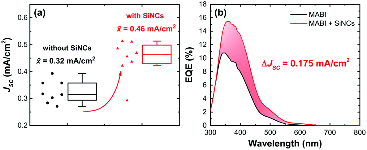 | ||
Fig. 6 Addition of silicon nanocrystals (SiNCs) to MABI solar cells. (a) Comparative study of the current density (JSC) of 8 control devices produced with MABI and 8 devices produced with a MABI and SiNCs composite. The data is presented as a standard box and whisker plot. Devices including SiNCs demonstrate a marked increase in JSC, and the mean (![[x with combining macron]](https://www.rsc.org/images/entities/i_char_0078_0304.gif) ) JSC is reported. (b) External quantum efficiency (EQE) for the best performing solar cells shown in (a). The EQE is shown for MABI alone (black curve) and for MABI with SiNCs (red curve). ) JSC is reported. (b) External quantum efficiency (EQE) for the best performing solar cells shown in (a). The EQE is shown for MABI alone (black curve) and for MABI with SiNCs (red curve). | ||
| Device | J SC (mA cm−2) | V OC (V) | FF | PCE (%) |
|---|---|---|---|---|
| MABI | 0.316 | 0.42 | 0.32 | 0.042 |
| MABI + SiNCs | 0.463 | 0.35 | 0.28 | 0.047 |
Due to the low concentration of the SiNCs, it is expected that they do not visibly contribute to absorption. The increased JSC observed in MABI devices with SiNCs over the control devices can be explained in two ways. In one view, the SiNCs act as a nucleation site for crystallization, thus improving the crystallinity of the MABI layer. The presence of impurities during crystallization is known to influence crystal growth.73–76 The efficiency of MABI devices has also previously been reported to be dependent on crystallinity of the MABI layer through optimization of the precursor solution concentration.60 It has been demonstrated that the addition of a small quantity (up to 0.3 mol%) of Al3+ ions enhances crystal growth in MAPbI3 perovskites leading to more reproducible device performance and higher PCE.77 Copper phthalocyanine (CuPc) nanocrystals have also been demonstrated to improve the crystallization of P3HT leading to higher device performance typically by increasing the JSC.78
We therefore used XRD to investigate the effect of adding SiNCs to the crystallinity of MABI. Fig. 7 shows the XRD spectra for a MABI thin film with and without SiNCs, deposited on quartz glass by spin coating. The concentration of SiNCs was the same as for the solar cell devices. The MABI layer containing SiNCs displayed a higher XRD peak intensity indicating improved crystallisation, with even extended crystal orientation in the [001] direction (Fig. 7a). The spectra were then normalised to the main peak at 24.55° (Fig. 7b). The MABI layers with SiNCs revealed a narrowing of the peak confirming increased crystal quality and extended crystal orientation. However, we did not observe any visible changes in film formation and there were no significant surface morphological changes on the basis of SEM analysis (ESI Fig. S8†). The SEM images revealed that crystals with a hexagonal cross-section of approximately 25 μm in diameter were present at the surface; these have been previously characterized as being single crystals of MABI.52 Unfortunately, quantitative and reliable estimates of the grain size from XRD could not be determined due to the grain size being far larger than the valid range for the Scherrer equation79 (calculated values were 79.1 nm for the MABI layer and 190.8 nm for MABI + SiNCs layer; these values are however affected by large errors due to the full-width at half maximum being very small, Fig. 7b). Therefore these results show that the addition of SiNCs has improved the overall crystallization, however without significant changes to the macroscale top surface morphology of the film.
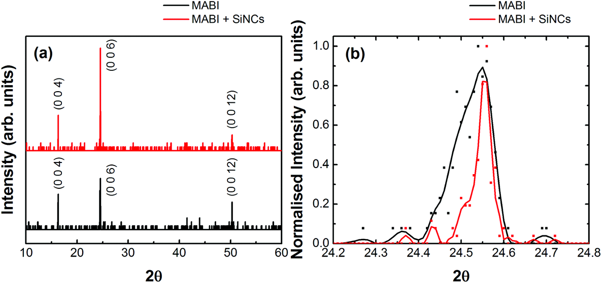 | ||
| Fig. 7 X-ray diffraction (XRD) spectra for MABI solar cells with and without Silicon nanocrystals (SiNCs). (a) Full scans and (b) normalised to the main peak at approximately 24.55°. In (b), the raw data is displayed as data points and the curves have been fitted to the data points. | ||
It has been reported that MAPbI3 device performance is related to the grain sizes and grain boundaries.80–82 In particular, larger MAPbI3 grains result in greater device performance,80 and the separation and transport of carriers was shown to occur at grain boundaries.81,82 We can therefore expect that also in MABI, larger crystal grains could have resulted in greater device performance. However, it should be noted that we could not confirm drastic changes in the grain size and that the crystal structure of MABI is fundamentally different to MAPbI3.
We therefore believe that the inclusion of the SiNCs resulted in an improvement in JSC, also through a different contribution as the addition of SiNCs can present a route for enhanced exciton dissociation. An increase in JSC can be achieved via assisted exciton dissociation by electron transfer into the SiNCs, increasing the likelihood of carrier separation and therefore reducing recombination losses. Fig. 8a shows the band structure of the MABI device with SiNCs and Fig. 8b illustrates exciton dissociation through electron transfer to a SiNC. It is expected that the dominant photo-generated species in MABI is a neutral bound e–h pair generated in the spatially separated Bi2I9 clusters. Charge transport under illumination occurs by excited electrons localised on Bi2I9 clusters tunnelling through MA+ barriers, owing to the high exciton binding energy. These neutral excitons can be dissociated from Coulomb attraction by an energetically favourable pathway for the electron to transfer onto an electron-accepting species such as p-type SiNCs. Excitons which are generated on Bi2I9 clusters close to SiNCs can be dissociated through electron transfer to a surface state on the nearby SiNCs, in a more favourable pathway than tunnelling through the MA+ barrier. The electron likely enters a high-lying surface state in the SiNC oxide layer with confined energy structure. The surface engineering by laser treatment performed on the SiNCs can provide passivation of trap defects such as dangling bonds on the SiNC surface,69 and an oxide layer has previously demonstrated enhanced carrier dissociation in SiNC:PTB7 hybrid solar cells.83 The Fermi level (EF) of surface-engineered SiNCs is approximately equal to the EF of MABI, therefore there is no potential barrier for carrier transfer.62,84 The free electron on the SiNC can also move through the MABI layer under the internal field.
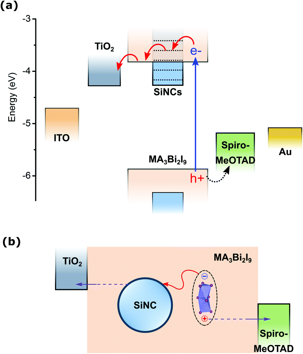 | ||
| Fig. 8 Energy band diagram and carrier extraction in MABI solar cells with silicon nanocrystals (SiNCs). (a) Schematic of non-equilibrated band diagram of the MABI device with SiNCs in energy (eV) relative to the vacuum level. The band edges were previously reported in the literature for MABI62 and SiNCs.84 (b) Schematic of the exciton dissociation through electron transfer to SiNCs. The dotted black line indicates a bound e–h pair localised on the Bi2I9 cluster. | ||
The performance of the devices after storage for 16 days in open air in the dark and a comparison of the median performance of the as-prepared devices and after 16 days are shown in the ESI (Fig. S5–S7†). There was no change in the rate of degradation of the MABI devices with and without SiNCs demonstrating that SiNCs do not adversely affect the stability of the MABI layer. As SiNCs can be easily oxidised in air, it is expected that the MABI also improves the stability of the SiNCs by providing encapsulation and restricting oxidation of the SiNCs. Therefore the combination of stable MABI with various types of nanocrystals is possible and should be explored.
4. Summary
We have demonstrated the high stability and hysteresis-less behaviour of the zero-dimensional hybrid material MABI for solar cell devices fabricated and stored in open air conditions. We expect that the absence of hysteresis is due to the spatially separated clusters of Bi2I9 bioctahedra with lower defect migration than conventional OTPs leading to reduced charge accumulation, and the higher tolerance of MABI to moisture and defects. The demonstration of hysteresis-less devices indicates reduced ionic motion in the MABI layer and suggests superior long-term stability over OTP devices. MABI devices with Au contacts were measured over a period of 21 days and present good stability when stored in open-air conditions in the dark. We observe a contact degradation process for MABI devices fabricated with Ag contacts caused by the interaction of Ag with the MABI layer. In addition, we have successfully improved the JSC of MABI solar cell devices through the addition of SiNCs to the MABI active layer forming a bulk hetero-architecture. We expect that the enhancement in JSC is due to improved crystallization and possibly the facilitation of exciton dissociation. The results highlight new opportunities for composite zero-dimensional materials where suitable energy level alignment could lead to beneficial synergies. In this sense, this study has shown that MABI coupled with SiNCs represent a novel architecture that could lead to efficient exploitation of carrier multiplication and third-generation mechanisms.Conflicts of interest
There are no conflicts to declare.Acknowledgements
This work was supported by EPSRC (EP/K022237/1 and EP/M024938/1) and by the New Energy and Industrial Technology Development Organization (NEDO). The authors declare no competing financial interests.References
- A. Kojima, K. Teshima, Y. Shirai and T. Miyasaka, Organometal Halide Perovskites as Visible-Light Sensitizers for Photovoltaic Cells, J. Am. Chem. Soc., 2009, 131(17), 6050–6051 CrossRef CAS PubMed.
- National Renewable Energy Laboratory. Best Research-Cell Efficiency table http://www.nrel.gov/pv/assets/images/efficiency_chart.jpg (accessed Apr 22, 2017).
- H. S. Jung and N.-G. Park, Perovskite Solar Cells: From Materials to Devices, Small, 2015, 11(1), 10–25 CrossRef CAS PubMed.
- T. Baikie, Y. Fang, J. M. Kadro, M. Schreyer, F. Wei, S. G. Mhaisalkar, M. Graetzel and T. J. White, Synthesis and Crystal Chemistry of the Hybrid Perovskite (CH3NH3)PbI3 for Solid-State Sensitised Solar Cell Applications, J. Mater. Chem. A, 2013, 1(18), 5628–5641 CAS.
- G. Xing, N. Mathews, S. Sun, S. S. Lim, Y. M. Lam, M. Gratzel, S. Mhaisalkar and T. C. Sum, Long-Range Balanced Electron- and Hole-Transport Lengths in Organic-Inorganic CH3NH3PbI3, Science, 2013, 342(6156), 344–347 CrossRef CAS PubMed.
- S. D. Stranks, G. E. Eperon, G. Grancini, C. Menelaou, M. J. P. Alcocer, T. Leijtens, L. M. Herz, A. Petrozza and H. J. Snaith, Electron-Hole Diffusion Lengths Exceeding 1 Micrometer in an Organometal Trihalide Perovskite Absorber, Science, 2013, 342(6156), 341–344 CrossRef CAS PubMed.
- Q. Dong, Y. Fang, Y. Shao, P. Mulligan, J. Qiu, L. Cao and J. Huang, Solar Cells. Electron-Hole Diffusion Lengths >175 Mm in Solution-Grown CH3NH3PbI3 Single Crystals, Science, 2015, 347(6225), 967–970 CrossRef CAS PubMed.
- Q. Lin, A. Armin, R. C. R. Nagiri, P. L. Burn and P. Meredith, Electro-Optics of Perovskite Solar Cells, Nat. Photonics, 2014, 9(2), 106–112 CrossRef.
- G. Xing, N. Mathews, S. S. Lim, N. Yantara, X. Liu, D. Sabba, M. Grätzel, S. Mhaisalkar and T. C. Sum, Low-Temperature Solution-Processed Wavelength-Tunable Perovskites for Lasing, Nat. Mater., 2014, 13(5), 476–480 CrossRef CAS PubMed.
- M. Saliba, T. Matsui, K. Domanski, J.-Y. Seo, A. Ummadisingu, S. M. Zakeeruddin, J.-P. Correa-Baena, W. R. Tress, A. Abate, A. Hagfeldt and M. Gratzel, Incorporation of Rubidium Cations into Perovskite Solar Cells Improves Photovoltaic Performance, Science, 2016, 354(6309), 206–209 CrossRef CAS PubMed.
- M. Saliba, T. Matsui, J.-Y. Seo, K. Domanski, J.-P. Correa-Baena, N. Mohammad K., S. M. Zakeeruddin, W. Tress, A. Abate, A. Hagfeldt and M. Gratzel, Cesium-Containing Triple Cation Perovskite Solar Cells: Improved Stability, Reproducibility and High Efficiency, Energy Environ. Sci., 2016, 9, 1989–1997 CAS.
- N. J. Jeon, J. H. Noh, W. S. Yang, Y. C. Kim, S. Ryu, J. Seo and S. I. Seok, Compositional Engineering of Perovskite Materials for High-Performance Solar Cells, Nature, 2015, 517(7535), 476–480 CrossRef CAS PubMed.
- X. Li, D. Bi, C. Yi, J.-D. Decoppet, J. Luo, S. M. Zakeeruddin, A. Hagfeldt and M. Gratzel, A Vacuum Flash-Assisted Solution Process for High-Efficiency Large-Area Perovskite Solar Cells, Science, 2016, 353(6294), 58–62 CrossRef CAS PubMed.
- N. Ahn, K. Kwak, M. S. Jang, H. Yoon, B. Y. Lee, J.-K. Lee, P. V. Pikhitsa, J. Byun and M. Choi, Trapped Charge-Driven Degradation of Perovskite Solar Cells, Nat. Commun., 2016, 7, 13422 CrossRef CAS PubMed.
- H. L. Clever and F. J. Johnston, The Solubility of Some Sparingly Soluble Lead Salts: An Evaluation of the Solubility in Water and Aqueous Electrolyte Solution, J. Phys. Chem. Ref. Data, 1982, 9(3), 751–784 CrossRef.
- C.-Y. Chang, W.-K. Huang and Y.-C. Chang, Highly-Efficient and Long-Term Stable Perovskite Solar Cells Enabled by a Cross-Linkable N -Doped Hybrid Cathode Interfacial Layer, Chem. Mater., 2016, 28(17), 6305–6312 CrossRef CAS.
- I. Deretzis, A. Alberti, G. Pellegrino, E. Smecca, F. Giannazzo, N. Sakai, T. Miyasaka and A. La Magna, Atomistic Origins of CH3NH3PbI3 Degradation to PbI2 in Vacuum, Appl. Phys. Lett., 2015, 106(13), 131904 CrossRef.
- S. Wang, Y. Jiang, E. J. Juarez-Perez, L. K. Ono and Y. Qi, Accelerated Degradation of Methylammonium Lead Iodide Perovskites Induced by Exposure to Iodine Vapour, Nat. Energy, 2016, 2(December), 395–398 Search PubMed.
- J. Li, Q. Dong, N. Li and L. Wang, Direct Evidence of Ion Diffusion for the Silver-Electrode-Induced Thermal Degradation of Inverted Perovskite Solar Cells, Adv. Energy Mater., 2017, 1602922 CrossRef.
- K. Domanski, J. P. Correa-Baena, N. Mine, M. K. Nazeeruddin, A. Abate, M. Saliba, W. Tress, A. Hagfeldt and M. Grätzel, Not All That Glitters Is Gold: Metal-Migration-Induced Degradation in Perovskite Solar Cells, ACS Nano, 2016, 10(6), 6306–6314 CrossRef CAS PubMed.
- A. Mei, X. Li, L. Liu, Z. Ku, T. Liu, Y. Rong, M. Xu, M. Hu, J. Chen, Y. Yang, M. Grätzel and H. Han, A Hole-Conductor-Free, Fully Printable Mesoscopic Perovskite Solar Cell with High Stability, Science, 2014, 345(6194), 295–298 CrossRef CAS PubMed.
- D. W. deQuilettes, W. Zhang, V. M. Burlakov, D. J. Graham, T. Leijtens, A. Osherov, V. Bulović, H. J. Snaith, D. S. Ginger and S. D. Stranks, Photo-Induced Halide Redistribution in Organic–inorganic Perovskite Films, Nat. Commun., 2016, 7(May), 11683 CrossRef CAS PubMed.
- B. Wu, K. Fu, N. Yantara, G. Xing, S. Sun, T. C. Sum and N. Mathews, Charge Accumulation and Hysteresis in Perovskite-Based Solar Cells: An Electro-Optical Analysis, Adv. Energy Mater., 2015, 5(19), 1500829 CrossRef.
- E. T. Hoke, D. J. Slotcavage, E. R. Dohner, A. R. Bowring, H. I. Karunadasa and M. D. McGehee, Reversible Photo-Induced Trap Formation in Mixed-Halide Hybrid Perovskites for Photovoltaics, Chem. Sci., 2015, 6(1), 613–617 RSC.
- J. J. Choi, X. Yang, Z. M. Norman, S. J. L. Billinge and J. S. Owen, Structure of Methylammonium Lead Iodide Within Mesoporous Titanium Dioxide: Active Material in High-Performance Perovskite Solar Cells, Nano Lett., 2014, 14(1), 127–133 CrossRef CAS PubMed.
- N. J. Jeon, J. H. Noh, Y. C. Kim, W. S. Yang, S. Ryu and S. I. Seok, Solvent Engineering for High-Performance Inorganic–organic Hybrid Perovskite Solar Cells, Nat. Mater., 2014, 13(9), 897–903 CrossRef CAS PubMed.
- Y. Yuan and J. Huang, Ion Migration in Organometal Trihalide Perovskite and Its Impact on Photovoltaic Efficiency and Stability, Acc. Chem. Res., 2016, 49(2), 286–293 CrossRef CAS PubMed.
- J. M. Ball and A. Petrozza, Defects in Perovskite-Halides and Their Effects in Solar Cells, Nat. Energy, 2016, 1(11), 16149 CrossRef CAS.
- M. Kulbak, D. Cahen and G. Hodes, How Important Is the Organic Part of Lead Halide Perovskite Photovoltaic Cells? Efficient CsPbBr3 Cells, J. Phys. Chem. Lett., 2015, 6(13), 2452–2456 CrossRef CAS PubMed.
- G. E. Eperon, G. M. Paternò, R. J. Sutton, A. Zampetti, A. A. Haghighirad, F. Cacialli and H. J. Snaith, Inorganic Caesium Lead Iodide Perovskite Solar Cells, J. Mater. Chem. A, 2015, 3(39), 19688–19695 CAS.
- T. S. Ripolles, K. Nishinaka, Y. Ogomi, Y. Miyata and S. Hayase, Efficiency Enhancement by Changing Perovskite Crystal Phase and Adding a Charge Extraction Interlayer in Organic Amine Free-Perovskite Solar Cells Based on Cesium, Sol. Energy Mater. Sol. Cells, 2016, 144, 532–536 CrossRef CAS.
- P. Luo, W. Xia, S. Zhou, L. Sun, J. Cheng, C. Xu and Y. Lu, Solvent Engineering for Ambient-Air-Processed, Phase-Stable CsPbI 3 in Perovskite Solar Cells, J. Phys. Chem. Lett., 2016, 7(18), 3603–3608 CrossRef CAS PubMed.
- F. Hao, C. C. Stoumpos, D. H. Cao, R. P. H. Chang and M. G. Kanatzidis, Lead-Free Solid-State Organic–inorganic Halide Perovskite Solar Cells, Nat. Photonics, 2014, 8(6), 489–494 CrossRef CAS.
- N. K. Noel, S. D. Stranks, A. Abate, C. Wehrenfennig, S. Guarnera, A.-A. Haghighirad, A. Sadhanala, G. E. Eperon, S. K. Pathak, M. B. Johnston, A. Petrozza, L. M. Herz and H. J. Snaith, Lead-Free Organic-Inorganic Tin Halide Perovskites for Photovoltaic Applications, Energy Environ. Sci., 2014, 7(9), 3061–3068 CAS.
- F. Hao, C. C. Stoumpos, P. Guo, N. Zhou, T. J. Marks, R. P. H. Chang and M. G. Kanatzidis, Solvent-Mediated Crystallization of CH3NH3SnI3 Films for Heterojunction Depleted Perovskite Solar Cells, J. Am. Chem. Soc., 2015, 137(35), 11445–11452 CrossRef CAS PubMed.
- S. J. Lee, S. S. Shin, Y. C. Kim, D. Kim, T. K. Ahn, J. H. Noh, J. Seo and S. I. Seok, Fabrication of Efficient Formamidinium Tin Iodide Perovskite Solar Cells through SnF2–Pyrazine Complex, J. Am. Chem. Soc., 2016, 138(12), 3974–3977 CrossRef CAS PubMed.
- M. R. Filip and F. Giustino, Computational Screening of Homovalent Lead Substitution in Organic-Inorganic Halide Perovskites, J. Phys. Chem. C, 2016, 120(1), 166–173 CAS.
- H. Tsai, W. Nie, J.-C. Blancon, C. C. Stoumpos, R. Asadpour, B. Harutyunyan, A. J. Neukirch, R. Verduzco, J. J. Crochet, S. Tretiak, L. Pedesseau, J. Even, M. A. Alam, G. Gupta, J. Lou, P. M. Ajayan, M. J. Bedzyk, M. G. Kanatzidis and A. D. Mohite, High-Efficiency Two-Dimensional Ruddlesden–Popper Perovskite Solar Cells, Nature, 2016, 536(7616), 312–316 CrossRef CAS PubMed.
- M. I. Saidaminov, O. F. Mohammed and O. M. Bakr, Low-Dimensional-Networked Metal Halide Perovskites: The Next Big Thing, ACS Energy Lett., 2017, 2(4), 889–896 CrossRef CAS.
- L. N. Quan, M. Yuan, R. Comin, O. Voznyy, E. M. Beauregard, S. Hoogland, A. Buin, A. R. Kirmani, K. Zhao, A. Amassian, D. H. Kim and E. H. Sargent, Ligand-Stabilized Reduced-Dimensionality Perovskites, J. Am. Chem. Soc., 2016, 138(8), 2649–2655 CrossRef CAS PubMed.
- C. Eames, J. M. Frost, P. R. F. Barnes, B. C. O'Regan, A. Walsh and M. S. Islam, Ionic Transport in Hybrid Lead Iodide Perovskite Solar Cells, Nat. Commun., 2015, 6, 7497 CrossRef CAS PubMed.
- S. Meloni, T. Moehl, W. Tress, M. Franckevičius, M. Saliba, Y. H. Lee, P. Gao, M. K. Nazeeruddin, S. M. Zakeeruddin, U. Rothlisberger and M. Graetzel, Ionic Polarization-Induced Current–voltage Hysteresis in CH3NH3PbX3 Perovskite Solar Cells, Nat. Commun., 2016, 7(May 2015), 10334 CrossRef CAS PubMed.
- W. Tress, N. Marinova, T. Moehl, S. M. Zakeeruddin, M. K. Nazeeruddin and M. Grätzel, Understanding the Rate-Dependent J–V Hysteresis, Slow Time Component, and Aging in CH3NH3PbI3 Perovskite Solar Cells: The Role of a Compensated Electric Field, Energy Environ. Sci., 2015, 8(3), 995–1004 CAS.
- S. Van Reenen, M. Kemerink and H. J. Snaith, Modeling Anomalous Hysteresis in Perovskite Solar Cells, J. Phys. Chem. Lett., 2015, 6(19), 3808–3814 CrossRef CAS PubMed.
- T. Leijtens, G. E. Eperon, N. K. Noel, S. N. Habisreutinger, A. Petrozza and H. J. Snaith, Stability of Metal Halide Perovskite Solar Cells, Adv. Energy Mater., 2015, 5(20), 1500963 CrossRef.
- R. Yu, D. Yang, X. Zhou, R. Yang, Z. Yang, W. Yu, X. Wang, C. Li, S. Liu and R. Chang, Surface Optimization to Eliminate Hysteresis for Record Efficiency Planar Perovskite Solar Cells, Energy Environ. Sci., 2016, 3(i), 1–10 Search PubMed.
- Y. Shao, Z. Xiao, C. Bi, Y. Yuan and J. Huang, Origin and Elimination of Photocurrent Hysteresis by Fullerene Passivation in CH3NH3PbI3 Planar Heterojunction Solar Cells, Nat. Commun., 2014, 5, 5784 CrossRef CAS PubMed.
- I. Levine, P. K. Nayak, J. T.-W. Wang, N. Sakai‡, S. Van Reenen, T. M. Brenner, S. Mukhopadhyay, H. J. Snaith, G. Hodes and D. Cahen, Interface-Dependent Ion Migration/Accumulation Controls Hysteresis in MAPbI3 Solar Cells, J. Phys. Chem. C, 2016, 120(30), 16399–16411.
- L. Zhao, X. Wang, X. Li, W. Zhang, X. Liu, Y. Zhu, H.-Q. Wang and J. Fang, Improving Performance and Reducing Hysteresis in Perovskite Solar Cells by Using F8BT as Electron Transporting Layer, Sol. Energy Mater. Sol. Cells, 2016, 157, 79–84 CrossRef CAS.
- R. L. Milot, G. E. Eperon, H. J. Snaith, M. B. Johnston and L. M. Herz, Temperature-Dependent Charge-Carrier Dynamics in CH3NH3PbI3 Perovskite Thin Films, Adv. Funct. Mater., 2015, 25(39), 6218–6227 CrossRef CAS.
- D. Li, G. Wang, H.-C. Cheng, C.-Y. Chen, H. Wu, Y. Liu, Y. Huang and X. Duan, Size-Dependent Phase Transition in Methylammonium Lead Iodide Perovskite Microplate Crystals, Nat. Commun., 2016, 7, 11330 CrossRef CAS PubMed.
- M. Abulikemu, S. Ould-Chikh, X. Miao, E. Alarousu, B. Murali, G. O. Ngongang Ndjawa, J. Barbé, A. El Labban, A. Amassian and S. Del Gobbo, Optoelectronic and Photovoltaic Properties of the Air-Stable Organohalide Semiconductor (CH3NH3)3Bi2I9, J. Mater. Chem. A, 2016, 4(32), 12504–12515 CAS.
- R. D. Schaller and V. I. Klimov, High Efficiency Carrier Multiplication in PbSe Nanocrystals: Implications for Solar Energy Conversion, Phys. Rev. Lett., 2004, 92(18), 186601 CrossRef CAS PubMed.
- R. J. Ellingson, M. C. Beard, J. C. Johnson, P. Yu, O. I. Micic, A. J. Nozik, A. Shabaev, A. L. Efros, R. J. Ellingson, M. C. Beard, J. C. Johnson, P. Yu, O. I. Micic, A. J. Nozik, A. Shabaev and A. L. Efros, Highly Efficient Multiple Exciton Generation in Colloidal PbSe and PbS Quantum Dots, Nano Lett., 2005, 5(5), 865–871 CrossRef CAS PubMed.
- M. C. Beard, K. P. Knutsen, P. Yu, J. M. Luther, Q. Song, W. K. Metzger, R. J. Ellingson and A. J. Nozik, Multiple Exciton Generation in Colloidal Silicon Nanocrystals, Nano Lett., 2007, 7(8), 2506–2512 CrossRef CAS PubMed.
- F. Hu, B. Lv, C. Yin, C. Zhang, X. Wang, B. Lounis and M. Xiao, Carrier Multiplication in a Single Semiconductor Nanocrystal, Phys. Rev. Lett., 2016, 116(10), 106404 CrossRef PubMed.
- D. Timmerman, I. Izeddin, P. Stallinga, I. N. Yassievich and T. Gregorkiewicz, Space-Separated Quantum Cutting with Silicon Nanocrystals for Photovoltaic Applications, Nat. Photonics, 2008, 2(2), 105–109 CrossRef CAS.
- C. Ni, G. Hedley, J. Payne, V. Svrcek, C. McDonald, L. K. Jagadamma, P. Edwards, R. Martin, G. Jain, D. Carolan, D. Mariotti, P. Maguire, I. Samuel and J. Irvine, Charge Carrier Localised in Zero-Dimensional (CH3NH3)3Bi2I9 Clusters, Nat. Commun., 2017, 8(1), 170 CrossRef PubMed.
- R. L. Z. Hoye, R. E. Brandt, A. Osherov, V. Stevanovic, S. D. Stranks, M. W. B. Wilson, H. Kim, A. J. Akey, J. D. Perkins, R. C. Kurchin, J. R. Poindexter, E. N. Wang, M. G. Bawendi, V. Bulovic and T. Buonassisi, Methylammonium Bismuth Iodide as a Lead-Free, Stable Hybrid Organic-Inorganic Solar Absorber, Chem. – Eur. J., 2016, 22(8), 2605–2610 CrossRef CAS PubMed.
- X. Zhang, G. Wu, Z. Gu, B. Guo, W. Liu, S. Yang, T. Ye, C. Chen, W. Tu and H. Chen, Active-Layer Evolution and Efficiency Improvement of (CH3NH3)3Bi2I9-Based Solar Cell on TiO2-Deposited ITO Substrate, Nano Res., 2016, 9(10), 2921–2930 CrossRef CAS.
- T. Singh, A. Kulkarni, M. Ikegami and T. Miyasaka, Effect of Electron Transporting Layer on Bismuth-Based Lead-Free Perovskite (CH3NH3)3Bi2I9 for Photovoltaic Applications, ACS Appl. Mater. Interfaces, 2016, 8(23), 14542–14547 CAS.
- M. Lyu, J. H. Yun, M. Cai, Y. Jiao, P. V. Bernhardt, M. Zhang, Q. Wang, A. Du, H. Wang, G. Liu and L. Wang, Organic–inorganic Bismuth(III)-Based Material: A Lead-Free, Air-Stable and Solution-Processable Light-Absorber beyond Organolead Perovskites, Nano Res., 2016, 9(3), 692–702 CrossRef CAS.
- B. W. Park, B. Philippe, X. Zhang, H. Rensmo, G. Boschloo and E. M. J. Johansson, Bismuth Based Hybrid Perovskites A3Bi2I9 (A: Methylammonium or Cesium) for Solar Cell Application, Adv. Mater., 2015, 27(43), 6806–6813 CrossRef CAS PubMed.
- T. Kawai and S. Shimanuki, Optical Studies of (CH3NH3)3Bi2I9 Single Crystals, Phys. Status Solidi, 1993, 177(1), 43–45 CrossRef.
- M. Pazoki, M. B. Johansson, H. Zhu, P. Broqvist, T. Edvinsson, G. Boschloo and E. M. J. Johansson, Bismuth Iodide Perovskite Materials for Solar Cell Applications: Electronic Structure, Optical Transitions, and Directional Charge Transport, J. Phys. Chem. C, 2016, 120(51), 29039–29046 CAS.
- V. Švrček, M. Kondo, K. Kalia and D. Mariotti, Photosensitive Self-Assembled Nanoarchitectures Containing Surfactant-Free Si Nanocrystals Produced by Laser Fragmentation in Water, Chem. Phys. Lett., 2009, 478(4–6), 224–229 CrossRef.
- V. Švrček, D. Mariotti, Y. Shibata and M. Kondo, A Hybrid Heterojunction Based on Fullerenes and Surfactant-Free, Self-Assembled, Closely Packed Silicon Nanocrystals, J. Phys. D: Appl. Phys., 2010, 43(41), 415402 CrossRef.
- S. Mitra, S. Cook, V. Švrček, R. A. Blackley, W. Zhou, J. Kovač, U. Cvelbar and D. Mariotti, Improved Optoelectronic Properties of Silicon Nanocrystals/polymer Nanocomposites by Microplasma-Induced Liquid Chemistry, J. Phys. Chem. C, 2013, 117(44), 23198–23207 CAS.
- V. Svrcek, D. Mariotti, U. Cvelbar, G. Filipič, M. Lozac'h, C. McDonald, T. Tayagaki and K. Matsubara, Environmentally Friendly Processing Technology for Engineering Silicon Nanocrystals in Water with Laser Pulses, J. Phys. Chem. C, 2016, 120(33), 18822–18830 CAS.
- Y. Yuan, J. Chae, Y. Shao, Q. Wang, Z. Xiao, A. Centrone and J. Huang, Photovoltaic Switching Mechanism in Lateral Structure Hybrid Perovskite Solar Cells, Adv. Energy Mater., 2015, 5(15), 1500615 CrossRef.
- J. M. Azpiroz, E. Mosconi, J. Bisquert and F. De Angelis, Defect Migration in Methylammonium Lead Iodide and Its Role in Perovskite Solar Cell Operation, Energy Environ. Sci., 2015, 8(7), 2118–2127 CAS.
- Y. Kato, L. K. Ono, M. V. Lee, S. Wang, S. R. Raga and Y. Qi, Silver Iodide Formation in Methyl Ammonium Lead Iodide Perovskite Solar Cells with Silver Top Electrodes, Adv. Mater. Interfaces, 2015, 2(13), 2–7 Search PubMed.
- P. M. Martins, F. A. Rocha and P. Rein, The Influence of Impurities on the Crystal Growth Kinetics according to a Competitive Adsorption Model, Cryst. Growth Des., 2006, 6(12), 2814–2821 CAS.
- C. M. Pina, Inhibition of Growth in Solid Solution–aqueous Solution Systems by Non-Incorporating Impurities, Surf. Sci., 2011, 605(5), 545–550 CrossRef CAS.
- E. Allahyarov, K. Sandomirski, S. U. Egelhaaf and H. Löwen, Crystallization Seeds Favour Crystallization Only during Initial Growth, Nat. Commun., 2015, 6, 7110 CrossRef CAS PubMed.
- S. Veintemillas-Verdaguer, Chemical Aspects of the Effect of Impurities in Crystal Growth, Prog. Cryst. Growth Charact. Mater., 1996, 32(1), 75–109 CrossRef CAS.
- J. T.-W. Wang, Z. Wang, S. K. Pathak, W. Zhang, D. DeQuilettes, F. Wisnivesky, J. Huang, P. Nayak, J. Patel, H. Yusof, Y. Vaynzof, R. Zhu, I. Ramirez, J. Zhang, C. Ducati, C. Grovenor, M. Johnston, D. S. Ginger, R. Nicholas and H. Snaith, Efficient Perovskite Solar Cells by Metal Ion Doping, Energy Environ. Sci., 2016, 9(9), 2892–2901 CAS.
- Y. Zhang and Z. Wei, Enhancing the Performance of Polymer Solar Cells Using CuPc Nanocrystals as Additives, Nanotechnology, 2015, 26(20), 204001 CrossRef PubMed.
- L. Alexander and H. P. Klug, Determination of Crystallite Size with the X-Ray Spectrometer, J. Appl. Phys., 1950, 21(2), 137–142 CrossRef CAS.
- H. D. Kim, H. Ohkita, H. Benten and S. Ito, Photovoltaic Performance of Perovskite Solar Cells with Different Grain Sizes, Adv. Mater., 2016, 28(5), 917–922 CrossRef CAS PubMed.
- J. S. Yun, A. Ho-Baillie, S. Huang, S. H. Woo, Y. Heo, J. Seidel, F. Huang, Y. B. Cheng and M. A. Green, Benefit of Grain Boundaries in Organic-Inorganic Halide Planar Perovskite Solar Cells, J. Phys. Chem. Lett., 2015, 6(5), 875–880 CrossRef CAS PubMed.
- J. S. Yun, J. Seidel, J. Kim, A. M. Soufiani, S. Huang, J. Lau, N. J. Jeon, S. I. Seok, M. A. Green and A. Ho-Baillie, Critical Role of Grain Boundaries for Ion Migration in Formamidinium and Methylammonium Lead Halide Perovskite Solar Cells, Adv. Energy Mater., 2016, 6, 1600330 CrossRef.
- Y. Ding, M. Sugaya, Q. Liu, S. Zhou and T. Nozaki, Oxygen Passivation of Silicon Nanocrystals: Influences on Trap States, Electron Mobility, and Hybrid Solar Cell Performance, Nano Energy, 2014, 10, 322–328 CrossRef CAS.
- T. Velusamy, S. Mitra, M. Macias-Montero, V. Svrcek and D. Mariotti, Varying Surface Chemistries for P-Doped and N-Doped Silicon Nanocrystals and Impact on Photovoltaic Devices, ACS Appl. Mater. Interfaces, 2015, 7(51), 28207–28214 CAS.
Footnote |
| † Electronic supplementary information (ESI) available. See DOI: 10.1039/c7nr05764d |
| This journal is © The Royal Society of Chemistry 2017 |