
 Open Access Article
 This Open Access Article is licensed under a
 Creative Commons Attribution 3.0 Unported Licence
Capacitive pressure sensing with suspended graphene–polymer heterostructure membranes†
Christian
Berger
 a,
Rory
Phillips
a,
Alba
Centeno
b,
Amaia
Zurutuza
b and
Aravind
Vijayaraghavan
*a
a,
Rory
Phillips
a,
Alba
Centeno
b,
Amaia
Zurutuza
b and
Aravind
Vijayaraghavan
*a
aSchool of Materials and National Graphene Institute, University of Manchester, Manchester, M13 9PL, UK. E-mail: aravind@manchester.ac.uk
bGraphenea S.A., 20018 Donostia-San Sebastián, Spain
First published on 6th November 2017
Abstract
We describe the fabrication and characterisation of a capacitive pressure sensor formed by an ultra-thin graphene–polymer heterostructure membrane spanning a large array of micro-cavities each up to 30 μm in diameter with 100% yield. Sensors covering an area of just 1 mm2 show reproducible pressure transduction under static and dynamic loading up to pressures of 250 kPa. The measured capacitance change in response to pressure is in good agreement with calculations. Further, we demonstrate high-sensitivity pressure sensors by applying a novel strained membrane transfer and optimising the sensor architecture. This method enables suspended structures with less than 50 nm of air dielectric gap, giving a pressure sensitivity of 123 aF Pa−1 mm−2 over a pressure range of 0 to 100 kPa.
Introduction
Capacitive pressure sensors are used for a broad range of applications due to their high pressure sensitivity, low temperature dependence and low power consumption.1,2 A capacitive pressure sensor typically comprises a thin conductive membrane which is freely suspended above a fixed counter-electrode in a parallel plate geometry, where the space is filled with either air or a vacuum.3 In this configuration, a higher sensitivity is achieved by increasing the suspended membrane area, reducing the dielectric gap and using a membrane material with a lower bulk elastic modulus. However, this increases the size of the sensor, resulting in nonlinear pressure transduction and a limited dynamic operating range.4Existing capacitive pressure sensors employ either silicon-based or polymer-based suspended membranes that are on the order of microns in thickness, therefore requiring relatively large diameters of several 100s of microns and capacitor spacing below 1 μm in order to give a sufficiently high sensitivity.3,5 In view of improving the performance of these devices, the fabrication of large area membranes with a smaller air gap often results in membrane collapse driven by either capillary forces or stiction due to electrostatics or van der Waals forces during the fabrication or operation of the device.6,7 This limits current technologies from achieving higher sensitivities and reduces their reliability.
Emerging ultra-thin nanomaterials such as carbon nano-membranes, cross-linked gold nanoparticles and the family of 2-dimensional (2-d) materials have shown great potential as candidates for next generation nano- and micro-electromechanical systems (MEMS and NEMS).8–10 Amongst these, single-layer graphene is regarded as a promising material for pressure sensing due to its large-area processability by chemical vapour deposition (CVD), high conductivity, high elasticity and excellent tensile strength.11,12 Moreover, early studies on graphene have shown that when suspended across a micro-cavity etched into silicon oxide, the graphene exhibits an ultra-strong adhesion to the surface and thereby seals the micro-cavity off from the surrounding atmosphere.13,14 This property also holds for other 2-d materials, including CVD graphene, due to their atomic thickness and negligible bending rigidity.15 The opportunity of forming gas tight membranes with almost negligible bending rigidity and its potential for developing pressure sensitive devices from graphene has prompted many efforts into fabricating suspended CVD graphene devices.16–21
The most common method of forming suspended CVD graphene structures is to transfer the graphene from its parent substrate (on which it is synthesised) onto a cavity-baring substrate using a sacrificial polymer support film.22,23 However, in a manner similar to current capacitive pressure sensor devices, devices often collapse due to stiction or capillary forces that act on the graphene during the removal of the polymer support.20,21 Additional processing steps have been developed to overcome this fabrication challenge. For example, solvents are exchanged in order to reduce capillary forces,24 critical-point drying protocols are applied25 and samples are annealed after transfer.26 Alternatively, support-free transfer methods such as wet-contact printing,27 face-to-face transfer28 and transfers facilitated by self-assembled monolayers29 have also been developed. Whilst such methods increase the probability of individual graphene membranes to remain suspended after transfer, they do not provide a complete solution for a 100% yield of suspended graphene structures over a large area.
Another strategy in preventing the collapse of suspended graphene is to reinforce membranes with another material.30–32 For example, by stacking up multiple layers of CVD graphene on top of one another or by depositing carbon nanotubes on a graphene film, crack-free freestanding structures up to 1.5 mm in diameter and 5.1 nm thickness have been demonstrated.33,34 However, this approach requires many fabrication steps, is very time consuming and results in wrinkling of the suspended membranes. Most recently, graphene–polymer heterostructure membranes comprising single-layer CVD graphene and an ultra-thin polymer layer, 10s of nanometres in thickness, have been shown to provide an excellent support for facilitating suspended graphene devices with 100% yield.35 Whilst the presence of a polymer on the surface of graphene is often a disadvantage in chemical and bio-medical sensing applications (where a clean surface of graphene is crucial to providing a high sensitivity),36 as a mechanical component it provides an optimal trade-off between the elastic modulus and membrane yield.37
Further, a route towards minimising membrane stiction in NEMS switches is to reduce the gate electrode contact area by implementing 3-dimensional gate electrode geometries.38,39 For example, CVD graphene closely suspended over an electrode with a ‘line contact’ has been demonstrated with reliable radio frequency actuation at low operating voltages.7 In the present work, we fabricate, characterise and test capacitive pressure sensors comprising an array of ultra-thin graphene–polymer heterostructure membranes and demonstrate a route towards high sensitivity pressure sensors over a large pressure range using a modified transfer method and a 3-dimensional cavity structure.
Results
Fabrication of sensor arrays
Sensors are fabricated from CVD graphene grown on copper foils (provided by Graphenea), following a two-step transfer process; the CVD graphene is first transferred from a square piece of copper foil of 5 mm × 5 mm size on to a flat silicon dioxide surface of a silicon substrate (SiO2/Si) using a polymethylmethacrylate (PMMA) transfer polymer and a wet transfer process described in ESI Discussion 1† and elsewhere.22 On a separate substrate, the SiO2 surface of a 1 cm × 1 cm piece of Si/SiO2 wafer is patterned by deep reactive ion etching (DRIE) to form an array of circular or hexagonal holes of a given diameter, periodicity and depth, arranged in various patterns such as a hexagonally packed lattice. On the surface of this chip, surrounding the region of perforation, metal electrodes are formed using a photomask and thermal metal evaporation. The chip with the CVD graphene on the surface is then coated with a layer of PMMA photoresist (PR) (Fig. 1, step 1) and a tape support window is adhered to its top surface. The support and graphene-PMMA stack is then lifted off the SiO2 surface using an aqueous potassium hydroxide etchant (Fig. 1, step 2). We do not directly transfer the graphene from the copper foil onto the perforated substrate because the PMMA coating on the copper is not homogeneous. Moreover, a homogenous coating of polymer on the graphene, as achieved by a two-step transfer process, is required for the optimal design and operation of the sensor array as will be described subsequently. In the final step the flattened graphene–polymer membrane is aligned with the patterned SiO2 surface using a tape supported transfer process described elsewhere (Fig. 1, step 4).22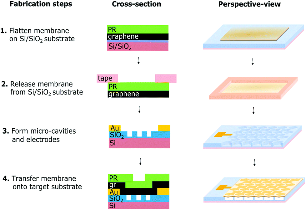 | ||
| Fig. 1 Fabrication steps and schematics of a graphene–polymer capacitive pressure sensor. | ||
Each sensor array now comprises a monolayer graphene membrane with a second polymer layer of total membrane thickness tm, suspended over an array of circular cavities each of diameter 2a and depth tgap. An additional SiO2 dielectric of thickness tox exists at the base of each cavity, beneath which lies the highly doped Si substrate which acts as the counter electrode. An array of such cavities covers an area of up to 1 mm2. Since the cavities are now sealed by the graphene membrane, an equilibrium pressure p0 exits within each cavity. When the external pressure is changed to a value p > p0 (positive pressure), the membrane deflects in to the cavity and the centre of the membrane achieves a deflection of z. The deflection of the membrane results in a change in capacitance which is measured and correlated to the change in pressure. A detailed description of the entire fabrication protocol is given in ESI Discussion 1.†
Modelling of graphene capacitive pressure sensors
The deflection mechanics of suspended membranes structures is typically described by either a non-linear membrane model (z ≫ tm) or a linear plate model (z < tm), where z is the typical membrane. Whilst the non-linear model assumes in-plane stretching as the dominant factor determining the deflection of the membrane, the linear plate model solely considers out-of-plane bending. Throughout this study we employ membranes with a thickness of approximately 140 nm and measure deflections of 10s of nanometers as characterised in a previous study.35 Thus, the deflection profile of the membrane is approximated by the plate model given by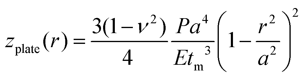 | (1) |
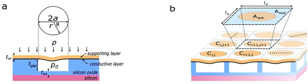 | ||
| Fig. 2 Dimensions of a capacitive pressure sensor. (a) A schematic cross-section of a capacitive pressure sensor comprising a conductive layer and a supporting layer suspended over a cavity etched into a Si/SiO2 substrate. (b) A schematic in perspective view of a capacitive pressure sensor array with unit cells in row i and column j with a capacitance value of Ci, j. | ||
A unit cell of a pressure sensing device is defined by two areal components; a suspended area, Asus and a surrounding substrate supported area, Asup as shown in Fig. 2b. In this analysis the suspended area is defined by a circle with radius a and the total unit cell area is defined by
| Aunit = Asus + Asup = lx × ly. | (2) |
The total capacitance of a unit cell in an array is then given by
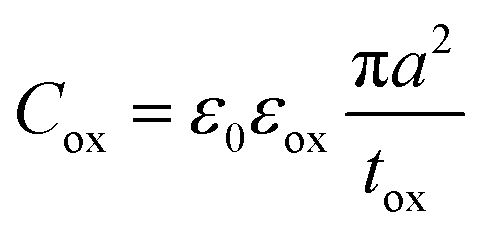
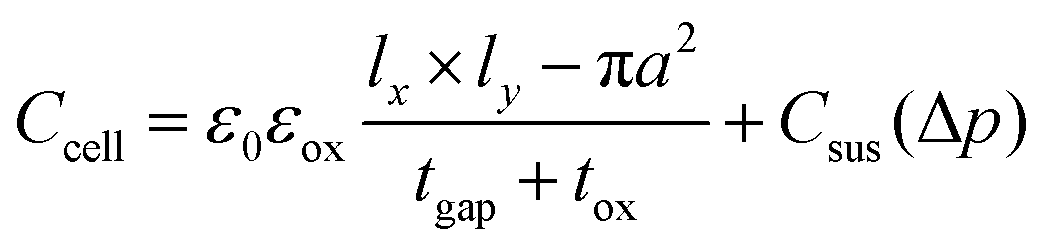 | (3) |
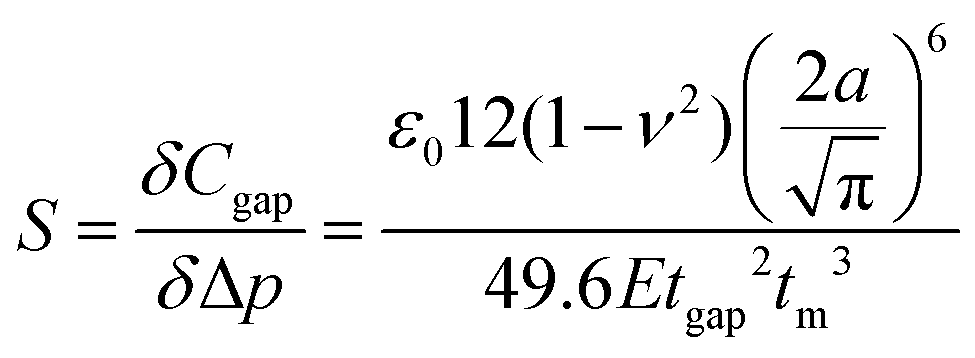
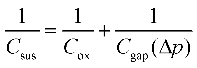 | (4) |
 and Cgap is the capacitance of the air gap given by the integral
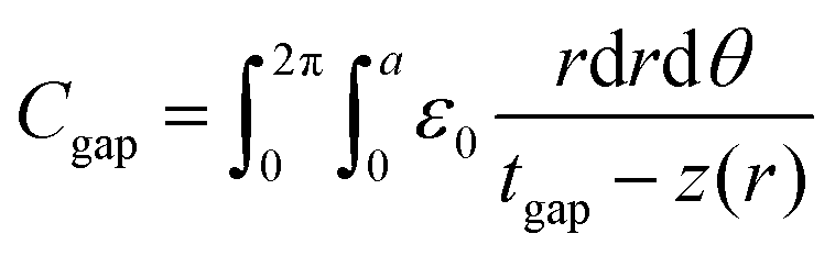 | (5) |
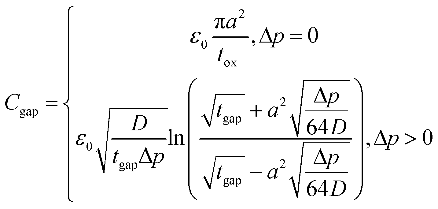 | (6) |
A similar analysis has also been shown for square plates.41 The capacitance of an entire device with an array of N × M pressure sensing cells is thus given by summing over all of the rows i and columns j of the array given by
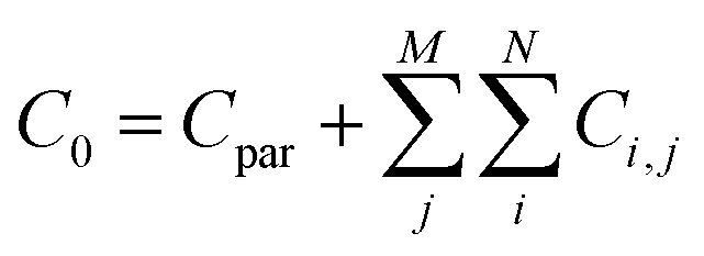 | (7) |
 | (8) |
Whilst this model provides a basic description of a pressure sensor array, in practice numerous other effects play a role in determining a pressure sensor's performance. A summary of these effects can be captured by an equivalent circuit model of the pressure sensor.
The fabrication protocol outlined in Fig. 1 was used to fabricate two different designs of pressure sensor. The thickness of the polymer layer used in both of these designs was calibrated such that 100% yield of suspended membranes can be achieved in both devices, whilst maintaining a high deflection sensitivity of the membranes and thus a measureable capacitance signal. This calibration procedure is outlined our previous study on graphene–polymer membranes.35 The first design uses a thick SiO2 layer, deep cavities and relatively small membranes as shown in Fig. 3a.i. This design uses a straightforward circular cavity geometry, in order to confirm that the experimental device behaviour fits the electromechanical model. The second design uses a thin SiO2 layer, shallow cavities, relatively large membranes and micro-bumps in the cavities as shown in Fig. 3a.ii. This design is to optimise the deflection sensitivity and electromechanical coupling of the pressure sensor. The micro-bumps in the cavity act as an anti-stiction surface for the membrane as explained in a later discussion. In the first part of this work we will only be concerned with design 1 in order to experimentaly verify the electromechanical model above.
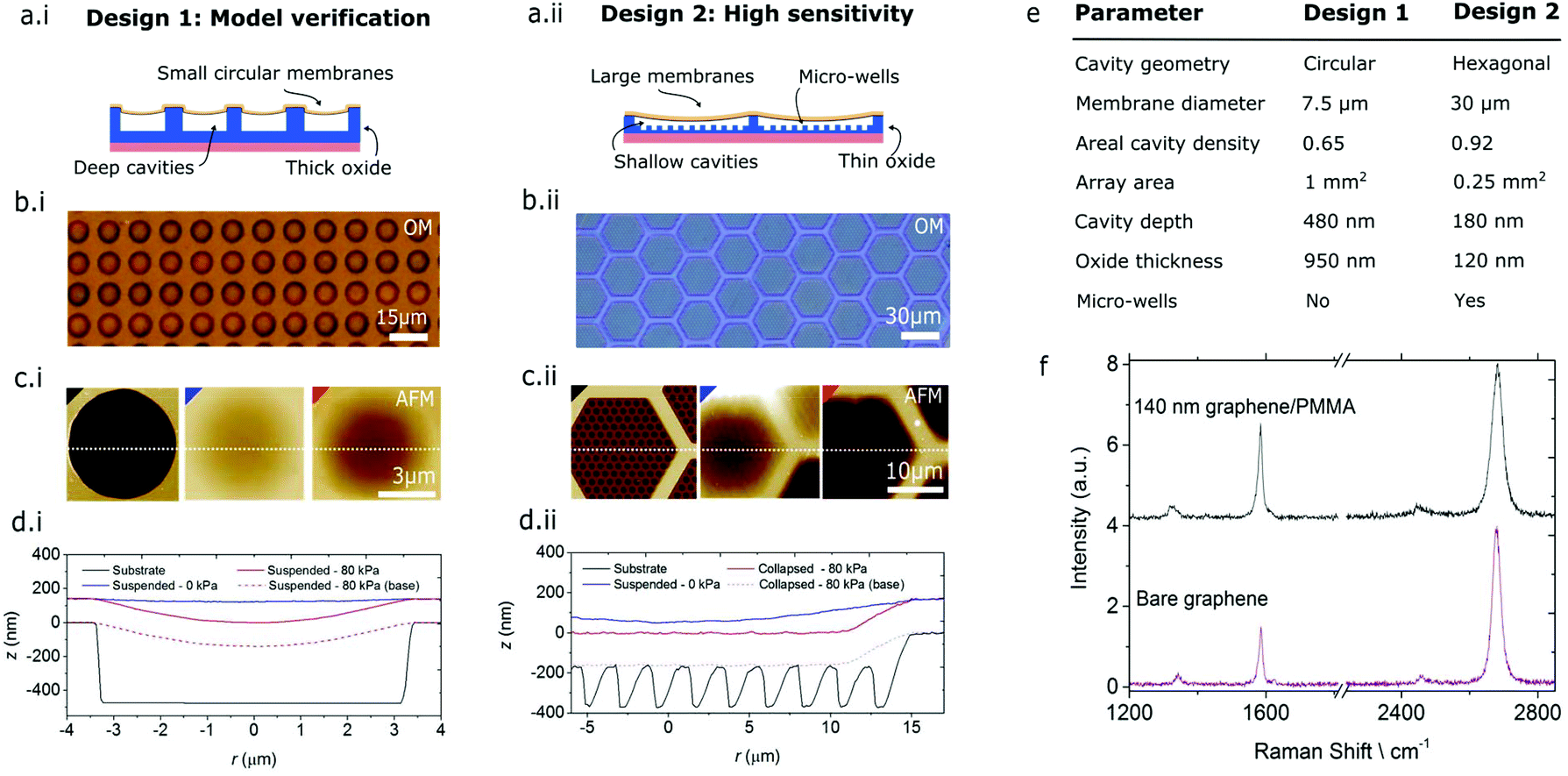 | ||
| Fig. 3 Characterisation of graphene–polymer membrane arrays. (a) Schematic of membrane arrays of (i) design for model verification and (ii) high sensitivity devices. (b) Optical micrographs (OM) of suspended membrane arrays at 50× magnification directly after fabrication, (c) AFM height maps and (d) cross-sections of a single cavity before transfer (black – bare substrate), a suspended graphene–polymer membrane at equilibrium pressure (blue – suspended – 0 kPa) and when pressurised to 80 kPa (red – suspended – 80 kPa) respectively. (e) A summary table of the device dimensions of design 1 and 2. (f) The Raman spectrum of a substrate supported graphene–polymer film and a bare substrate supported graphene film. | ||
Physical properties of sensor arrays
Identifying the number of inactive membranes, that have either collapsed or contain cracks, is crucial in modelling the pressure sensor performance. In order to characterise the membrane integrity over large areas, we employed a series of optical and mechanical techniques. Sensors were first imaged by optical microscopy to check for rips, cracks or contaminants in the graphene–polymer film. A detailed description of these common artifacts is given in ESI Discussion 2.†Fig. 3b.i shows an optical micrograph in reflective-mode at 50× magnification. On this scale we can identify that all membranes are homogenous and contaminant free. Samples with full coverage and a homogenous film transfer were subsequently analysed by atomic force microscopy (AFM) and Raman spectroscopy. The AFM height maps and cross-sections in Fig. 3c.i and d.i show that the suspended membrane gently sags 5 nm below the level of the supported film surface at equilibrium. Moreover, when the cavity is pressurised to 80 kPa using a micro-blister inflation technique, the membrane deflects 135 nm below the level of the supported film surface. The dimensions of each of the devices, as measured by AFM, are summarised in Fig. 3e. Further characterisations of successfully transferred films is undertaken by AFM Quantitative Nanomechanical Mapping (QNM).43 This mode of AFM allows us to create high resolution maps of the height and effective elastic modulus of our device, highlighting cracks or tears in the suspended membranes which are not normally visible from Raman mapping. The micro-blister inflation technique is also used to probe the gas permeability of the membranes. This is discussed in further detail in ESI Discussion 3.†Fig. 3f shows the Raman spectrum of a supported graphene–polymer film in comparison to that of a bare graphene film. The two spectra demonstrating that the graphene layer in the composite film is of high quality apart from some minor defects as indicated by the presence of a D peak (1350 cm−1) intensity ratio. Further, Streamline™ Raman mapping allowed us to map the G and 2D-peak intensities over the entire sample area. A detailed discussion of the features revealed by this imaging mode is given in ESI Discussion 2.†Sensor device performance (device 1)
Fully characterised graphene–polymer membrane arrays with full coverage, 100% yield, minimal defects with dimensions as described in Fig. 3a and b were electrically contacted to a chip carrier and loaded into a custom built pressure system as shown in Fig. 4a. The pressure system consists of a pressure chamber equipped with pressure control valves and a reference pressure gauge, enabling precise control over the chamber pressure. Devices are first evacuated using a scroll pump, followed by a N2 gas purge, giving a stable and inert atmosphere inside the pressure chamber. In order to calibrate the drift of the capacitance, samples were measured for 1 hour at equilibrium pressure in a N2 atmosphere. During this period we observed a drift of 0.05% of the total capacitance. A detailed description of the pressure sensor calibration is given in ESI Discussion 4.† The pressure was then varied between atmospheric pressure (0 kPa pressure difference between inside and outside of the cavity) and 250 kPa at various speeds and time intervals in order to characterise the sensor response. As the pressure inside the chamber increases the suspended graphene–polymer membranes are pressed into the micro-cavities with a force proportional to the chamber pressure. The capacitance between the graphene layer and the doped silicon substrate is measured using a high precision LCR meter with a resolution of 1 fF in typical operating conditions. Capacitance measurements were taken at 1 kHz with a bias of 1 V, giving a noise limited capacitance accuracy of 0.05%. Devices were compared to identical devices fabricated in parallel, but without any cavities etched into the substrate. This allowed us to confirm that it is truly the deflection of suspended graphene–polymer membranes that is causing the change in capacitance, as shown in Fig. 4b. Each data set represents four cycles, with each cycle representing either a pump or vent between 0 kPa and 250 kPa. The device with cavities shows a strong correlation between the pressure and capacitance in comparison to the reference device without cavities. This demonstrates the device's sensitivity to pressure due to the presence of cavities and therefore suspended graphene–polymer membranes. We notice that for the device containing cavities, the capacitance response is offset by 15 ± 10 kPa. This offset is attributed relaxation of intrinsic ripples in the suspended membranes, which compensate membrane deflections at low pressures. We are able to extract the sensitivity of devices containing cavities from the slope of the curve in Fig. 4b as 0.21 ± 0.01 aF Pa−1.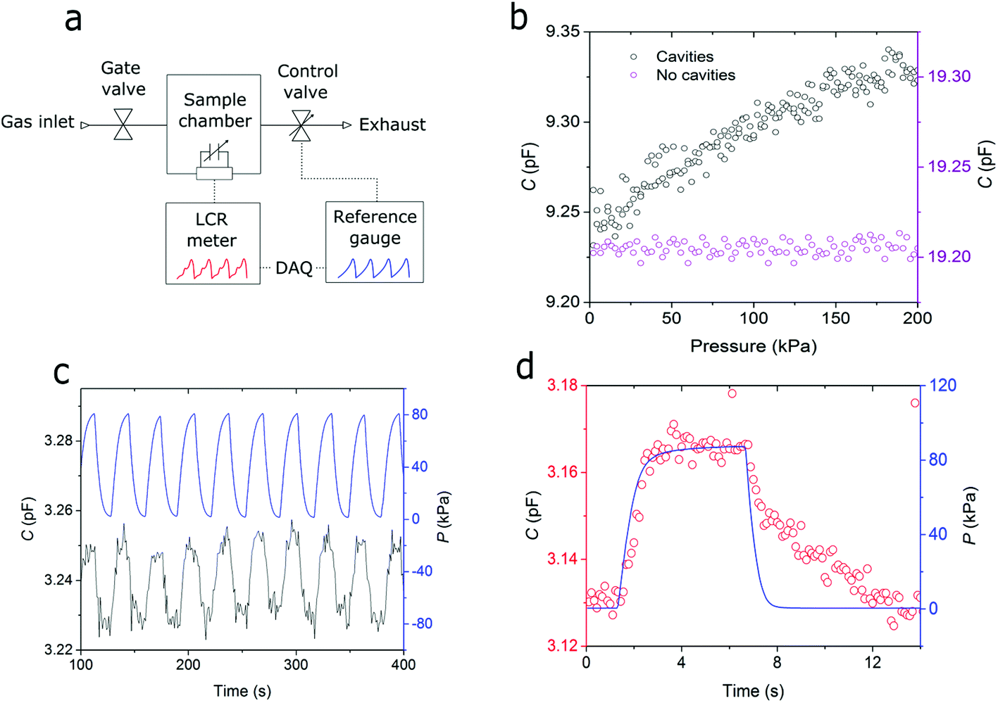 | ||
| Fig. 4 Performance of graphene–polymer membrane pressure sensor array. (a) A schematic of the measurement setup used to measure the capacitive pressure sensors. (b) Pressure versus capacitance measurements of a device with and without cavities. (c) Capacitance measurements of the pressure sensor in reference to 10 pressure cycles between 0 and 80 kPa at 30 seconds intervals. (d) The measured capacitance of the pressure sensor in reference to a 6 seconds pressure pulse. | ||
Next we cycled devices containing cavities between 20 kPa and 100 kPa with a cycling period of 30 seconds. Fig. 4c shows the reference pressure and measured capacitance of a device containing cavities over 10 cycles. The device's response to the continuous change in pressure is reproducible with a precision of 6% of the measured pressure range given by the standard deviation of the capacitance value measured during the cycling experiment. This irreproducibility is likely due to the air-flow within the pressure chamber creating movement of the graphene–polymer film's edges, thus creating irregular jumps in capacitance of the device. As the inaccuracy due to the sensors reproducibility dominates over other contributions such as the sensors linearity and hysteresis, we quote the accuracy of the sensor as 6%. Finally, we measured the capacitance of the sensor for a short pressure pulse of 6 seconds at 90 kPa in order to probe the sensor's response time. Fig. 4d shows that the measured capacitance and reference pressure signals correlate well and minimal drift is observed over the complete cycle. However, a delayed response is observed on the down-step of the pressure pulse giving a combined response time of the up and down pressure stroke of 1.8 s. We expect that the formation of ripples in the membrane has a smaller time scale than ripple relaxation. A similar effect was observed previously in micro-structured dielectric capacitive pressure sensors.44 In order to confirm that the observed capacitance change is solely due to the deflection of suspended graphene–polymer membranes and that gas concentrations are independent of the device capacitance, we also measured the samples without any cavities in different gaseous atmospheres (ESI Discussion 4†). We also note that the pressure sensor forms a low leakage capacitor with a discharge resistance of 6.5 MΩ when measured at an excitation of 1 V at 1 kHz. Assuming the discharge curve is linear this gives a discharge time of approximately 32 μs. As this time scale is an order of magnitude lower than the sampling rate of our capacitance measurements, we do not expect this to have a significant effect on our measurements.
Using the height profiles of membranes pressurised to different pressure values during micro-blister inflation tests, we were able to estimate the sensitivity of the capacitive sensor using the previously derived expression (eqn (8)). As each sensor contains several thousand membranes over a 1 mm x 1 mm square, we conducted AFM measurements at 5 randomly distributed 90 μm x 90 μm sample areas, giving an average distribution of membrane morphologies of each sensor. AFM measurements were taken immediately after pressure sensing experiments to ensure our calculation captures membranes that were definitely active during sensing. Using parameters from the table in Fig. 3e, the calculated sensitivity is 0.28 ± 0.8 aF Pa−1. The large error in our calculation is attributed to the variation in deflections of individual membranes. The significance of these variations for a capacitive pressure sensor are discussed in a later section. Further, the calculation is higher in comparison to the measured sensitivity of 0.21 ± 0.01 aF Pa−1. We attribute this difference to a combination of charge leakage through the SiO2 layer and along the surface of the sensor chip as well as due to the plate model being at its limit in the pressure used throughout our experiment.
The performance of this first demonstration of a capacitive pressure sensor remains low compared to current state of the art sensors; nonetheless this design serves to validate our experimental results with a model. For example, a recently published CMOS (complementary metal–oxide semiconductor) pressure sensor spanning an area of 0.31 mm2 as described in Table 1, has a sensitivity of 1.2 aF Pa−1.45 In the following section we outline a route towards high sensitivity pressure sensors and demonstrating an initial working prototype with a sensitivity of 5.0 aF Pa−1 over an area of just 0.04 mm2.
| Metal–polymer38 | Metal–silicon30 | Graphene–polymer(this work) | |
|---|---|---|---|
| Membrane matetial | Parylene C/AU/parylene | SiOx/Al/SiOx | CVD graphene/PMMA |
| Elastic modulus | 3.9 GPa | <100 GPa | 10.9 GPa |
| Membrane thickness | 1.3 μm/200 nm/1.3 μm | 500 nm/2 μm/500 nm | 0.35 nm/140 nm |
|
|
|
|
| Sensitivity at FPS | 2.2 aF Pa−1 | 1.2 aF Pa−1 | 4.2 aF Pa−1 |
| Areal sensitivity (mm2) | 25 aF Pa−1 | 4 aF Pa−1 | 123 aF Pa−1 |
| Full pressure scale (FPS) | 6.8 kPa | 600 kPa | 100 kPa |
High-performance sensor device (device 2)
The continuing challenge in achieving high sensitivity over a small area, whilst maintaining a large pressure range, is to minimise the air gap between the sensing membrane and the cavity bed. The minimal air gap distance is limited by three contributing factors that cause collapse of the membrane due to stiction to the bottom of the cavity. First, the induced dipoles due to the chemical functionalities of the membrane underside and the cavity bed cause attraction between the two conductive plates. We expect this effect to have negligible contribution to membrane stiction due to the inert nature of the materials used in our device design. Second, electrostatic forces due to applied potential bias or fabrication induced charging of the capacitor plates can result in membrane stiction. Whilst impedance measurements of the cavity-baring substrates indicate that our fabrication procedure has a minor influence on the charge density in the oxide layer, the measured values are insignificant towards attracting the graphene–polymer membrane. The third and most significant force acting on the membrane is due to retarded van der Waals forces, also known as Casimir forces. These forces are significant when membranes come into a proximity of d ≈ 100 nm to the bottom of the cavity.46 The pressure due to the Casmir force is given by | (9) |
In order to further improve the pull-in instability of the graphene–polymer capacitive pressure sensor we employed two additional steps to our fabrication protocol. First, micro-wells were etched into the base of the cavities in order to reduce the silicon oxide area below the suspended membrane, thereby reducing the total Casimir force acting on the membrane. Second, we applied a strain to the graphene–polymer membrane during the membrane transfer procedure in view of stiffening the membrane and therefore increasing the effective restoring force keff of deflected membranes. In addition, we also changed the shape of cavities to a hexagonal in order achieve high packing densities whilst preventing high local stresses as found in square shaped membranes.49 A schematic, optical micrograph and AFM of this optimised design is shown in Fig. 3a–d.ii. In addition a schematic of the strained transfer and an optical micrograph of the resulting suspended membrane structure in comparison to a normal membrane transfer are shown in Fig. 5. The schematic illustrates that crumpled graphene–polymer membranes as transferred using the standard method (Fig. 1) results in excess material that can readily adhere the to the cavity (Fig. 5a.ii). When these membranes are strained, such crumples are flattened out (Fig. 5b.i) and the membrane can span large areas without stiction to the cavity (Fig. 5b.ii). The optical micrographs shown in Fig. 5a.iii and b.iii show a change in contrast between collapsed and suspended membranes respectively due to applying strain during membrane transfer. The applied strain during transfer is estimated as 0.15 ± 0.01 by Raman spectroscopy as described in ESI Discussion 5.†
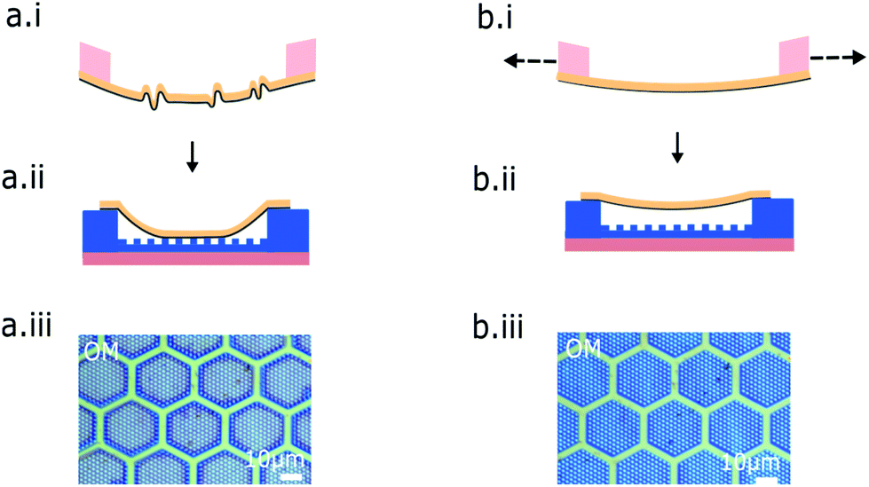 | ||
| Fig. 5 Strained film transfer. (i–ii) Schematic comparing normal membrane transfer (a) to strained membrane transfer (b). (iii) Optical micrographs taken at 50× magnification of the resultant samples when the normal (a) and strain transfer (b) are applied. | ||
The morphology of a bare micro-cavity, a suspended graphene–polymer membrane and a collapsed membrane are shown in Fig. 3a–d.ii. Taking the film thickness as 140 ± 4 nm we estimate that the graphene layer is suspended just 40 ± 4 nm above the oxide layer. Further comparison of the collapsed membrane with a cross-section of the bare micro-cavity reveals negligible adhesion to the sidewalls of the sub-cavities. This infers that the membrane is loosely bound to the bed of the micro-cavity, relying solely on the adhesion to the area remaining on the cavity bed. We were able to release collapsed membranes from the cavity base by retracting the transferred film and re-laminating the surface with applied strain as shown in the ESI Video.†
A sensor with device design 2 that was optimised for high sensitivity was tested in our pressure setup. The device performance was characterised using the same procedure as described previously apart from the maximum sensing pressure was limited to a maximum of 80 kPa in order to minimise permanent membrane stiction. Fig. 6 shows the sensitivity of a device with design 2 when cycled between 0 and 80 kPa at 30 seconds intervals in comparison to a device with design 1. A significant increase in performance is measured despite the sensing area occupying just 0.25 mm2 on the chip compared to 1 mm2 in the first device. However, cycling the sensor does not give the same degree of reproducibility in sensitivity as the first generation device. Further detail on the pressure testing data of design 2 is given in ESI Discussion 6.† The large variance in the second device's response is attributed to noise in the capacitance measurements which is likely due to charge leakage through the oxide and along the chip surface. We expect the majority contribution to originate from trapped states and mobile surface charge in the gate oxide as a result of the DRIE of sub-cavities. We support this assumption by comparison of the C–V characteristics of the two generations of devices as shown in ESI Discussion 7.† In order to reduce the noise level in future iterations we propose the use of a pinhole free dielectric or deposition of a barrier layer.
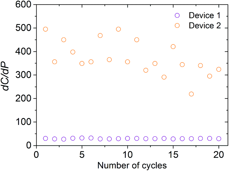 | ||
| Fig. 6 Comparison of the capacitance-pressure sensitivity of devices with design 1 and 2. | ||
Discussion
MEMS and NEMS technologies face the continuing challenge of achieving higher device sensitivities over large pressure ranges whilst covering a minimal area on chip. Existing and emerging devices employ either a silicon-based or a polymer-based active membrane. The device characteristics and performance of such state-of-the-art devices are compared to the graphene–polymer-based sensors in Table 1. The thickness and modulus of our proposed structures places the graphene–polymer sensors in the property space which currently includes polymer membranes, but also extends into the performance gap between polymer and silicon MEMS in terms of sensitivity and pressure range.In Table 1, the performance of graphene–polymer capacitive pressure sensors are compared. Metal–polymer pressure sensors typically involve membranes ranging in diameter from 500 μm up to several millimetres with polymer thicknesses of several microns encapsulating a thin metal layer (100–200 nm). The combination of a soft membrane material and large membrane diameter gives excellent sensitivity over a small pressure range. Such sensors are typically developed for biomedical applications where small pressure fluctuations in the body are monitored and the biocompatibility of the sensor's constituent materials are crucial. Metal–silicon pressure sensors with a membrane diameter of several hundred microns, consisting of a stack of two sub-micron thick SiO2 layers encapsulating a metal layer, are of a significantly higher stiffness. In addition, CMOS processing compatibility enables membranes to be suspended in close proximity to the complimentary electrode thereby giving a large sensing range whilst maintaining high sensitivity.
Graphene–polymer pressure sensors aim to cover the entire operating range for MEMS pressure sensors, including the areas occupied by high sensitivity, low range polymer sensors and low sensitivity, high range silicon sensors as well as bridging the gaps in performance between the two. Whilst our first iteration of devices demonstrate reproducible pressure sensing using graphene–polymer stacks as the active element, the large gap between the membrane and the complimentary doped silicon sensing electrode (1430 nm) gives a relatively low sensitivity. Devices with design 2 use a much thinner oxide layer in order to improve the electromechanical coupling of the graphene–polymer membrane, thereby improving the device sensitivity. Moreover, the pressure range (80 kPa) is maintained as the membrane diameter is kept considerably small and the membrane is pre-strained during the transfer procedure. The stiffness of the membranes used in all of these devices lies between that of silicon and polymer based MEMS (10.9 GPa) and the membrane transfer technique enables the fabrication of densely packed suspended membranes on the wafer scale. However, the elastic properties of the membrane can be varied with ease by modifying either the polymer thickness or number of graphene layers.35 For example, by using an even stiffer membrane in a similar architecture, as shown by design 2, there is scope to further extend the pressure range of graphene–polymer pressure sensors whilst maintaining a high sensitivity.
In addition to improving device sensitivity and range, the graphene–polymer membrane structure aims to overcome several reliability issues faced in current MEMS and NEMS technologies.47,50 First, the use of sacrificial layers in CMOS processing puts several limitations on device architecture and material design; materials must be resistant to aggressive etchants, have sufficient stability to overcome capillary forces, and an additional sealing step is required after removal of the sacrificial etchant.51,52 By transferring the active mechanical component directly onto a pre-patterned micro-cavity in air we avoid trapping liquids that initiate membrane collapse and completely seal the micro-cavity. Moreover, CMOS compatible polymers such as parylene-C have been shown to be equally valid for this fabrication process.53 A further challenge is presented by the brittle fatigue in silicon-based membranes.54 This failure mechanism is often attributed to stress corrosion cracking, whereby stress-assisted hydrolysis of the native or deposited SiO2 layer initiates crack propagation.50 Graphene and PMMA are both known to have reversible morphological changes in response to humidity and there is no indication of crack formation or propagation on cycling the pressure sensors.55–57
Whilst we recognise that the reproducibility and hence the accuracy of the graphene–polymer sensors are not comparable to state-of-the-art devices, the aim of the sensor principle is to improve the trade-off between sensitivity and pressure range of capacitive pressure sensors. We identify inaccuracies in the pressure cycling data as engineering challenges which will be addressed by refining the sensor fabrication technique and design. For example, by pre-patterning the CVD graphene before the polymer deposition step in the fabrication of the device, the exposure of graphene edges to the surrounding atmosphere is minimised. Further, the use of an oil-fill of the pressure sensor housing can be used to isolate the active sensing area.58 Both of these techniques are expected to significantly minimise noise in the capacitance signal.
A further performance inaccuracy in these sensors is the response time. We note that a delayed response time of the graphene–polymer pressure sensor is mostly apparent in the down stroke of a pressure cycle. As the deflection mechanism is dominated by the bending of the polymer component of the graphene–polymer membrane it is most appropriate to compare this response time to that of other polymer-based pressure sensors. The typical response time of polymer-based pressure sensors is on the order of 1–10 s which is primarily attributed to the relaxation time of the polymer matrix as it reconfigures into its equilibrium state.44,59 In contrast silicon-based the pressure sensors typically have a response time on the order of 10–100 ms due to the high stiffness and the crystalline nature of the material.60 Whilst the current sensor performance may not be suitable for the measurement of short pressure changes, such as in mobile hydraulics for example,61 the sensor may be more suitable for applications with long pressure cycles, such as level measurements or blood-pressure monitoring.62 In order to improve the sensor response time we propose to further reduce the thickness of the polymer layer as well as using crystalline polymer materials such as parylene-C that exhibit significantly faster relaxation times compared to the PMMA polymer that is currently used.
With the graphene–polymer pressure sensor in its early stage of development, it remains a challenge to accomplish a large area array of suspended membranes with uniform performance characteristics. Such non-uniformities arise from a combination of membrane relaxation and gas-leakage through defects in the membranes. The effects of membrane relaxation and gas-leakage have been investigated in previous micro-blister inflation experiments on graphene–polymer membranes. This study demonstrated that graphene–parylene-C membranes of thicknesses ranging from 23 nm to 201 nm have an excellent reproducibility in the deflection of individual membranes, but show a significant variation in the deflection between different membranes across a large area array. However, with respect to the performance of the capacitive pressure sensor these variations become averaged out due to the large quantity of membranes that operate in parallel across the entire array.
Increasing the number of cavities within the device therefore provides a strategy towards improving the reproducibility of the device, however this approach is limited due to the cost of increasing the device footprint by adding more cavities. A more direct approach to solve the issue of reproducibility is to improve the control over the method of laminating the graphene–polymer film onto the cavity-baring substrate, thus regulating the mechanical properties of the individual suspended membranes. Moreover, by further reducing the thickness of the polymer layer a reduction in gas-leakage can be obtained as previously shown in the aforementioned study on graphene–parylene-C membranes.
Beyond the initial demonstration of a capacitive pressure sensor, we aim to develop more sophisticated MEMS and NEMS devices using ultra-thin graphene–polymer membranes. The excellent elasticity and high temperature compatibility of graphene makes graphene–polymer membranes attractive for pressure sensing in harsh environments, where shock and elevated temperatures would cause significant damage to tradition silicon MEMS. Whilst we note that the polymer layer is likely to be the limiting material in harsh environment applications, the large variety of polymers available as ultra-thin coatings also allows us to fabricate a range of ultra-thin membranes with properties tuned to specific applications, where the polymer layer not only acts as a mechanical reinforcement but also gives additional functionality to the membrane.8,63 In view of the latter, we also envisage the use of graphene–polymer membranes in polymer MEMS devices ranging from micron-scale pumps and valves in micro-fluidics and lab-on-chip devices to pressure sensors and actuators in biomedical applications.
Conclusion
We have demonstrated the fabrication and characterisation protocol of graphene–polymer capacitive pressure sensor arrays. Using this method we fabricated two types of devices with different designs. The first device has large capacitor spacing and comprises an array of circular micro-cavities enabling low loss capacitance measurements and membrane deflections that are described by a simple linear elastic model. Thus, we show the device is well described by an analytical electromechanical model. We then demonstrate the fabrication of a second device that aims to improve the device sensitivity whilst maintaining a relatively large working pressure range. By applying strain to the membrane during transfer we are able to fabricate membranes 30 μm in diameter and suspended less than 50 nm above the surface of micro-cavities etched into silicon dioxide. This precision enables excellent electromechanical coupling giving an unprecedented pressure sensitivity of 123 aF Pa−1 mm−2 over a pressure scale of 80 kPa. Finally we discuss the current challenges in state of the art MEMS technologies and how graphene–polymer NEMS can enable highly sensitive devices with a large operating range and excellent reliability.Author contributions
AV & CB conceived and designed the experiments conducted data analysis and interpretation. CB & RP conducted fabrication. CB conducted characterisation and pressure experiments. CB, RP & AV contributed to drafting this manuscript.Conflicts of interest
The authors declare no competing financial interests.Acknowledgements
AV and CB acknowledge funding from the Engineering and Physical Science (EPSRC) Industrial Cooperative Awards in Science & Technology (I-CASE) grant number EP/L505547/1.References
- M. Narducci, L. Yu-Chia, W. Fang and J. Tsai, CMOS MEMS capacitive absolute pressure sensor, J. Micromech. Microeng., 2013, 23, 55007 CrossRef.
- Y. Zhang, S. Massoud-ansari, G. Meng, W. Kim and N. Najafi, An ultra-sensitive, high-vacuum absolute capacitive pressure sensor, Micro Electro Mech. Syst. (MEMS), 2001, 1, 166–169 Search PubMed.
- C. H. Mastrangelo, X. Zhang and W. C. Tang, Surface-Micromachined Capacitive Differential Pressure Sensor with Lithographically Defined Silicon Diaphragm, J. Microelectromech. Syst., 1996, 5, 98–105 CrossRef CAS.
- C. Hin-Leungm and K. D. Wise, Scaling Limits in Batch-Fabricated Silicon Pressure Sensors, IEEE Trans. Electron Devices, 1987, 34, 850–858 CrossRef.
- D. Y. Chiou, M. Y. Chen, M. W. Chang and H. C. Deng, Characterization and optimization design of the polymer-based capacitive micro-arrayed ultrasonic transducer, Jpn. J. Appl. Phys., Part 1, 2007, 46, 7496–7503 CrossRef CAS.
- O. I. Aydin, T. Hallam, J. L. Thomassin, M. Mouis and G. Duesberg, Challenges in Suspending CVD Graphene : More than Capillary Effects, IEEE Ultim. Integr. Silicon, 2014, 14, 33–36 Search PubMed.
- X. Liu, et al., Large Arrays and Properties of 3-Terminal Graphene Nanoelectromechanical Switches, Adv. Mater., 2014, 26, 1571–1576 CrossRef CAS PubMed.
- A. Castellanos-Gomez, V. Singh, H. S. J. van der Zant and G. a. Steele, Mechanics of freely-suspended ultrathin layered materials, Ann. Phys., 2015, 527, 27–44 CrossRef CAS.
- X. Zhang, A. Beyer and A. Gölzhäuser, Mechanical characterization of carbon nanomembranes from self-assembled monolayers, Beilstein J. Nanotechnol., 2011, 2, 826–833 CrossRef CAS PubMed.
- H. Schlicke, et al., Freestanding membranes of cross-linked gold nanoparticles: novel functional materials for electrostatic actuators, ACS Appl. Mater. Interfaces, 2015, 7, 15123–15128 CAS.
- G.-H. Lee, et al., High-strength chemical-vapor-deposited graphene and grain boundaries, Science, 2013, 340, 1073–1076 CrossRef CAS PubMed.
- D. Akinwande, et al., A review on mechanics and mechanical properties of 2D materials—Graphene and beyond, Extreme Mech. Lett., 2017, 13, 42–77 CrossRef.
- S. P. Koenig, N. G. Boddeti, M. L. Dunn and J. S. Bunch, Ultra-strong Adhesion of Graphene Membranes, Nat. Nanotechnol., 2011, 6, 543–546 CrossRef CAS PubMed.
- J. S. Bunch, et al., Impermeable Atomic Membranes from Graphene Sheets, Nano Lett., 2008, 8, 2458–2462 CrossRef CAS PubMed.
- N. Lindahl, et al., Determination of the Bending Rigidity of Graphene via Electrostatic Actuation of Buckled Membranes, Nano Lett., 2012, 12, 3526–3531 CrossRef CAS PubMed.
- Q. Wang, W. Hong and L. D, Graphene ‘Microdrums’ on Freestanding Perforated Thin Membrane for High Sensitivity MEMS Pressure Sensor, Nanoscale, 2016, 8, 7663–7671 RSC.
- S. Zhu, K. Ghatkesar, C. Zhang and G. C. A. M. Janssen, Graphene based piezoresistive pressure sensor, Appl. Phys. Lett., 2013, 102, 161904 CrossRef.
- J. Aguilera-Servin, T. Miao and M. Bockrath, Nanoscale pressure sensors realized from suspended graphene membrane devices, Appl. Phys. Lett., 2015, 106, 83103 CrossRef.
- S. J. Cartamil-Bueno, et al., Colorimetry Technique for Scalable Characterization of Suspended Graphene, Nano Lett., 2016, 6, 2416 Search PubMed.
- A. D. Smith, F. Niklaus, A. Paussa, S. Vaziri, A. C. Fischer, M. Sterner, F. Forsberg, A. Delin, D. Esseni, P. Palestri, M. Ostling and M. C. Lemme, Electromechanical Piezoresistive Sensing in Suspended Graphene Membranes, Nano Lett., 2013, 13, 3237–3242 CrossRef CAS PubMed.
- S. Lee, et al., A transparent bending-insensitive pressure sensor, Nat. Nanotechnol., 2016, 11, 1–8 CrossRef PubMed.
- J. W. Suk, et al., Transfer of CVD-Grown Monolayer Graphene onto Arbitrary Substrates, ACS Nano, 2011, 5, 6916–6924 CrossRef CAS PubMed.
- K. S. Kim, et al., Large-scale pattern growth of graphene films for stretchable transparent electrodes, Nature, 2009, 457, 706–710 CrossRef CAS PubMed.
- A. Yulaev, et al., Toward Clean Suspended CVD Graphene, RSC Adv., 2016, 6, 83954–83962 RSC.
- R. Maboudian, W. R. Ashurst and C. Carraro, Tribological challenges in micromechanical systems, Wear, 2002, 12, 95–100 Search PubMed.
- S. Wagner, et al., Graphene transfer methods for the fabrication of membrane-based NEMS devices, Microelectron. Eng., 2016, 159, 108–113 CrossRef CAS.
- B. Li, et al., Scalable Transfer of Suspended Two-Dimensional Single Crystals, Nano Lett., 2015, 15, 5089–5097 CrossRef CAS PubMed.
- L. Gao, et al., Face-to-face transfer of wafer-scale graphene films, Nature, 2014, 505, 190–194 CrossRef CAS PubMed.
- B. Wang, et al., Support-Free Transfer of Ultrasmooth Graphene Films Facilitated by Self-Assembled Monolayers for Electronic Devices and Patterns, ACS Nano, 2016, 10, 1404–1410 CrossRef CAS PubMed.
- X. Zang, Q. Zhou, J. Chang, Y. Liu and L. Lin, Graphene and carbon nanotube (CNT) in MEMS/NEMS applications, Microelectron. Eng., 2015, 132, 192–206 CrossRef CAS.
- D. Todorovi, A. Matkovi and M. Mili, Multilayer graphene condenser microphone, 2D Mater., 2015, 2, 1–6 Search PubMed.
- E. Sandoz-Rosado, E. D. Wetzel, J. T. Smith, S. Oida and J. Bai, The mechanical characterization of stacked, multilayer graphene cantilevers and plates, Proceedings of the 15th IEEE International Conference on Nanotechnology, 2016, 1, 37–40 Search PubMed.
- O. V. Martynov and M. Bockrath, Carbon nanotube stabilized single layer graphene cantilevers, Appl. Phys. Lett., 2017, 110, 151901–151905 CrossRef.
- Y.-M. Chen, et al., Ultra-large suspended graphene as highly elastic membrane for capacitive pressure sensor, Nanoscale, 2016, 6, 3555–3564 RSC.
- C. Berger, M. Dirschka and A. Vijayaraghavan, Ultra-thin graphene-polymer heterostructure membranes, Nanoscale, 2016, 8, 17928–17939 RSC.
- Y. Lin, et al., Clean Transfer of Graphene for Isolation and Suspension, ACS Nano, 2011, 5, 2362–2368 CrossRef CAS PubMed.
- S. Woo, et al., Realization of a High Sensitivity Microphone for a Hearing Aid Using a Graphene–PMMA Laminated Diaphragm, ACS Appl. Mater. Interfaces, 2017, 9, 1237–1246 CAS.
- J. O. Lee, et al., A sub-1-volt nanoelectromechanical switching device, Nat. Nanotechnol., 2012, 8, 36–40 CrossRef PubMed.
- S. M. Kim, et al., Suspended few-layer graphene beam electromechanical switch with abrupt on-off characteristics and minimal leakage current, Appl. Phys. Lett., 2011, 99, 23103 CrossRef.
- I. O. Wygant, M. Kupnik and B. T. Khuri-yakub, Analytically Calculating Membrane Displacement and the Equivalent Circuit Model of a Circular CMUT Cell, Proc. IEEE Ultrasonics Symp., 2008, 8, 2111–2114 Search PubMed.
- B. a. Ganji, Modeling of Capacitance and Sensitivity of a MEMS Pressure Sensor with Clamped Square Diaphragm, Int. J. Eng., 2013, 26, 1331–1336 Search PubMed.
- A. Lei, S. E. Diederichsen, M. Funding and M. B. Stuart, Dimensional Scaling for Optimized CMUT Operations, Proc. IEEE Ultrasonics Symp., 2014, 14, 2595–2598 Search PubMed.
- M. E. Dokukin and I. Sokolov, Quantitative Mapping of the Elastic Modulus of Soft Materials with HarmoniX and PeakForce QNM AFM Modes, Langmuir, 2012, 28, 16060–16071 CrossRef CAS PubMed.
- S. C. B. Mannsfeld, et al., Highly sensitive flexible pressure sensors with microstructured rubber dielectric layers, Nat. Mater., 2010, 9, 859–864 CrossRef CAS PubMed.
- F. Deng, Y. He, X. Wu and Z. Fu, A CMOS pressure sensor with integrated interface for passive RFID applications, Meas. Sci. Technol., 2014, 25, 125104 CrossRef.
- F. M. Serry, D. Walliser and G. J. Maclay, The role of the casimir effect in the static deflection and stiction of membrane strips in microelectromechanical systems (MEMS), J. Appl. Phys., 1998, 84, 2501 CrossRef CAS.
- U. Zaghloul, et al., Microelectronics Reliability On the reliability of electrostatic NEMS/MEMS devices : Review of present knowledge on the dielectric charging and stiction failure mechanisms and novel characterization methodologies, Microelectron. Reliab., 2011, 51, 1810–1818 CrossRef CAS.
- X. Liu, et al., Observation of Pull-In Instability in Graphene Membranes under Interfacial Forces, Nano Lett., 2013, 13, 2309–2313 CrossRef CAS PubMed.
- M. Engholm, T. Pedersen and E. V. Thomsen, Modeling of plates with multiple anisotropic layers and residual stress, Sens. Actuators, A, 2016, 240, 70–79 CrossRef CAS.
- W. Merlijn van Spengen, MEMS reliability from a failure mechanisms perspective, Microelectron. Reliab., 2003, 43, 1049–1060 CrossRef.
- B. Assadsangabi, X. Chen, D. Brox and K. Takahata, Microfabrication of Capacitive Pressure Sensors using Ferrofluid Sacrificial Layers, IEEE Sens., 2013, 13, 9 Search PubMed.
- T. Shibata, Y. Kitamoto, K. Unno and E. Makino, Micromachining of diamond film of MEMS applications, J. Microelectromech. Syst., 2000, 9, 47–51 CrossRef CAS.
- D. Ha, W. N. de Vries, S. W. M. John, P. P. Irazoqui and W. J. Chappell, Polymer-based miniature flexible capacitive pressure sensor for intraocular pressure (IOP) monitoring inside a mouse eye, Biomed. Microdevices, 2012, 14, 207–215 CrossRef CAS PubMed.
- O. M. Jadaan, N. N. Nemeth, J. Bagdahn and W. N. Sharpe, Probabilistic Weibull behavior and mechanical properties of MEMS brittle materials, J. Mater. Sci., 2003, 38, 4087–4113 CrossRef CAS.
- H. J. Jeong, et al., One-step transfer and integration of multifunctionality in CVD graphene by TiO2/graphene oxide hybrid layer, Small, 2014, 10, 2057–2066 CrossRef CAS PubMed.
- D. H. Ho, et al., Stretchable and Multimodal All Graphene Electronic Skin, Adv. Mater., 2016, 28, 2601–2608 CrossRef CAS PubMed.
- N. S. Tambe and B. Bhushan, Micro/nanotribological characterization of PDMS and PMMA used for BioMEMS/NEMS applications, Ultramicroscopy, 2005, 105, 238–247 CrossRef CAS.
- N. Lamberti, G. Caliano, A. Iula and A. S. Savoia, A high frequency cMUT probe for ultrasound imaging of fingerprints, Sens. Actuators, A, 2011, 172, 561–569 CrossRef CAS.
- A. G. P. Kottapalli, M. Asadnia, J. M. Miao, G. Barbastathis and M. S. Triantafyllou, A flexible liquid crystal polymer MEMS pressure sensor array for fish-like underwater sensing, Smart Mater. Struct., 2012, 21, 115030 CrossRef.
- J. C. Greenwood, Silicon in mechanical sensors, J. Phys. E: Sci. Intrum., 1988, 21, 1114–1128 CrossRef CAS.
- M. M. Sadeghi, R. L. Peterson and K. Najafi, High-speed electrostatic micro-hydraulics for sensing and actuation, Micro Electro Mech. Syst. (MEMS), 2013, 13, 1191–1194 Search PubMed.
- J. Park, et al., A Wireless Pressure Sensor Integrated with a Biodegradable Polymer Stent for Biomedical Applications, Sensors, 2016, 16, 809 CrossRef PubMed.
- C. M. Stafford, et al., Elastic Moduli of Ultrathin Amorphous Polymer Films, Macromolecules, 2006, 39, 5095–5099 CrossRef CAS.
Footnote |
| † Electronic supplementary information (ESI) available. See DOI: 10.1039/c7nr04621a |
| This journal is © The Royal Society of Chemistry 2017 |