
 Open Access Article
 This Open Access Article is licensed under a
 Creative Commons Attribution 3.0 Unported Licence
Polarisation-controlled single photon emission at high temperatures from InGaN quantum dots†
T.
Wang‡
 *a,
T. J.
Puchtler‡
*a,
T.
Zhu
b,
J. C.
Jarman
b,
L. P.
Nuttall
a,
R. A.
Oliver
b and
R. A.
Taylor
a
*a,
T. J.
Puchtler‡
*a,
T.
Zhu
b,
J. C.
Jarman
b,
L. P.
Nuttall
a,
R. A.
Oliver
b and
R. A.
Taylor
a
aDepartment of Physics, University of Oxford, Parks Road, Oxford, OX1 3PU, UK
bDepartment of Materials Science and Metallurgy, University of Cambridge, 27 Charles Babbage Road, Cambridge, CB3 0FS, UK. E-mail: tong.wang@physics.ox.ac.uk; tim.puchtler@physics.ox.ac.uk
First published on 29th June 2017
Abstract
Solid-state single photon sources with polarisation control operating beyond the Peltier cooling barrier of 200 K are desirable for a variety of applications in quantum technology. Using a non-polar InGaN system, we report the successful realisation of single photon emission with a g(2)(0) of 0.21, a high polarisation degree of 0.80, a fixed polarisation axis determined by the underlying crystallography, and a GHz repetition rate with a radiative lifetime of 357 ps at 220 K in semiconductor quantum dots. The temperature insensitivity of these properties, together with the simple planar epitaxial growth method and absence of complex device geometries, demonstrates that fast single photon emission with polarisation control can be achieved in solid-state quantum dots above the Peltier temperature threshold, making this system a potential candidate for future on-chip applications in integrated systems.
Introduction
Exploiting the quantum nature of light–matter interactions often relies on the presence of extreme conditions that cannot be applied outside the laboratory setting. In the case of polarised single photon emitters,1,2 most of today's systems rely on the presence of defects in 2D hexagonal boron nitride,3,4 diamond,5 silicon carbide,6 zinc oxide,7 or gallium nitride wafer8 to achieve polarised or un-polarised single photon generation beyond cryogenic temperatures. On the other hand, semiconductor quantum dots (QDs) possess the advantage that their dimension, geometry, and electrical contacting can be much more easily manipulated in the solid state. However, most QD literature reports are limited to temperatures below 10 K for the simultaneous observation of sub-Poissonian photon statistics9–12 and linearly polarised emission.13–24 In order to move towards the goal of practical integration into scalable electronic platforms, the reliance on material defects and low temperatures needs to be overcome. In particular, non-classical light sources based on solid-state QDs need to eventually break this temperature barrier and operate above the thermoelectric cooling threshold, typically around 200 K. Such systems would then in principle be the key building-blocks for truly secure on-chip quantum communication based on polarisation-reliant protocols, such as BB84,25 and act as qubit sources for linear optical quantum computing.26Much progress has been made on the investigation of high temperature operation of QD-based polarised single photon sources; several systems have demonstrated un-polarised single photon emission above this temperature barrier,13–15,27–31 with some even reaching operation temperatures beyond ambient conditions.31 On the other hand, polarisation control has been reported where either an external polariser is used, at the cost of 50% lower efficiency, or by the manipulation of device geometries to generate polarised photons with deterministic axes directly. The latter, albeit more desirable, has proven difficult to achieve, and has only been demonstrated at <10 K in pyramidal QDs,19 elliptical nanocolumns,16 or by the use of horizontally aligned nanowires.13–15,22 Similarly, high temperature single photon emission, regardless of polarisation control, is challenging to achieve. In order to produce an increased degree of quantum confinement to combat the thermal activation of non-radiative exciton decay pathways, it is often necessary to use both wide bandgap materials, such as III-nitrides,13–15,29–31 and highly confined QDs with extremely small dimensions grown via 3D fabrication routines, such as dot-in-a-nanowire systems.13,15,18,28,30,31 In these cases, although the use of nitrides allows large band-offsets, the commonly used conventional (0001) polar plane does not reliably produce a consistently high polarisation degree or deterministic polarisation direction,32 or exhibit polarisability at elevated temperatures. Polar nitrides also suffer from the influence of the quantum-confined Stark effect (QCSE), which can reduce the exciton oscillator strength and decrease the potential repetition rate. Furthermore, the reliance of complex device structures in achieving either polarised emission or high temperature single photon generation makes electrical contacting inevitably more laborious and integration of multiple devices or batch production inherently more difficult than planar epitaxial systems.
In this work, we report one such planar epitaxial solid-state QD system which achieves triggered single photon generation, linear polarised emission, a predefined polarisation axis, and a fast repetition rate at 220 K (−53 °C) simultaneously. The emission in the blue spectral region enables the use of efficient detectors,33 at a temperature reachable by commercial Peltier coolers. Our sample consists of non-polar (11−20) a-plane InGaN QDs grown by metal–organic vapour phase epitaxy (MOVPE) embedded within a p–i–n doped GaN matrix, allowing future fabrication of electrically pumped devices. Nanopillar structures, such as that shown in Fig. 1(a), were post processed for increased photon extraction efficiencies (see Experimental – Sample preparation for details). The ability to grow InGaN/GaN QDs on the a-plane minimises the unwanted QCSE, increases the exciton oscillator strength and radiative decay rate,34,35 reduces coupling to phonon-assisted non-radiative exciton decay routes,36 and causes highly polarised emission aligned to the [1−100] crystal axis,37 which we find to be temperature insensitive up to the Peltier cooling regime.
 | ||
| Fig. 1 (a) Schematic and scanning electron microscope image of a representative nanopillar structure in which QDs are embedded. (b) Temperature-dependent microphotoluminescence spectra at 4.7 K, and from 40 to 250 K at 30 K intervals, with peak intensities normalised to the emission at 4.7 K. | ||
Results and discussion
An example of the typical QD emission features measured using microphotoluminescence (μ-PL) can be seen in Fig. 1(b), exhibiting a single sharp peak at ∼2.58 eV at 4.7 K with a full width at half-maximum (FWHM) of 712 ± 68 μeV, attributed to the QD exciton, and a low-intensity background caused by the fragmented quantum well (QW) underlying the QDs arising from the growth method.34 As expected for a semiconductor QD exciton,38 the emission both redshifts and broadens in linewidth with increasing temperature, as evident in Fig. 1(b), due to the well-known bandgap shrinkage and exciton–phonon coupling respectively. At 220 K, the emission energy has redshifted to 2.54 eV, and its FWHM increased to 19.0 ± 0.4 meV.As the temperature increases, non-radiative recombination gradually becomes dominant, decreasing the emission intensity of the QD. As shown in Fig. 1(b) and 2(a), at 220 K, the peak intensity drops 30-fold and the integrated brightness decreases to 11% of that at 4.7 K. Measurement of the QD's integrated intensity at a much finer temperature step than Fig. 1(b) is recorded in Fig. 2(a), and studied with a standard single-channel Arrhenius-type equation that describes the thermally assisted intensity decay in semiconductors,
 | (1) |
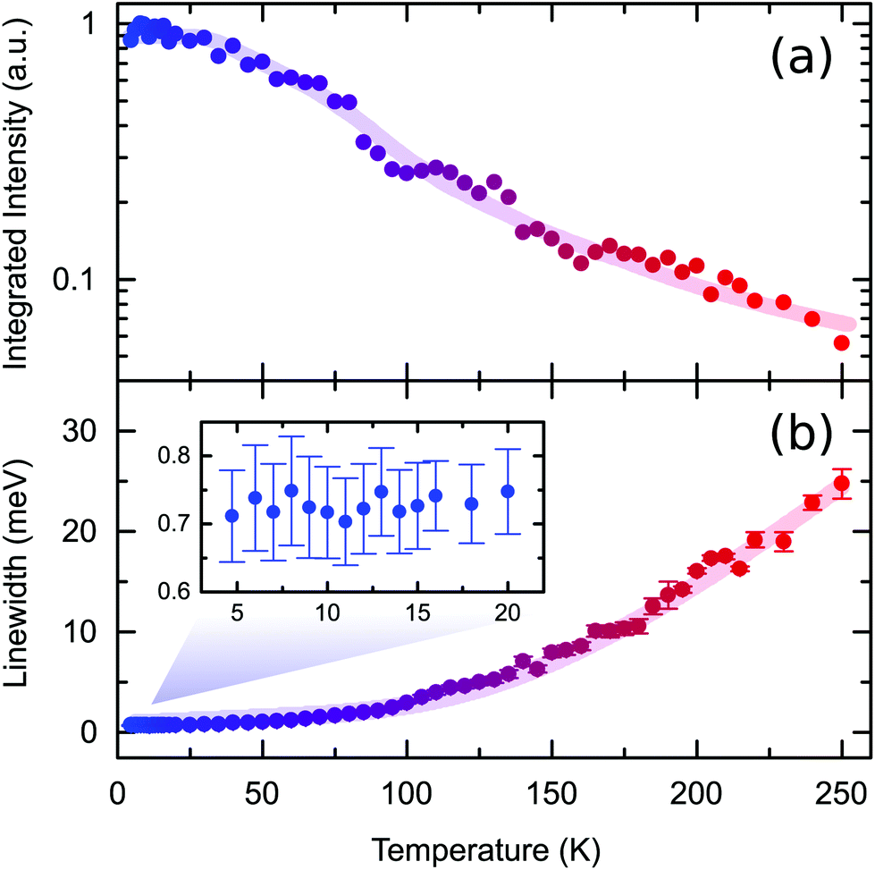 | ||
| Fig. 2 (a) Thermal quenching of normalised integrated intensity from 4.7 to 250 K. The experimental data was fitted with a standard single-channel Arrhenius-type intensity decay model. The vertical axis has been shown on a logarithmic scale for more lucid presentation of the integrated intensity at elevated temperatures. (b) Phonon and spectral diffusion assisted broadening of the exciton transition linewidth and fitting with a standard semiconductor linewidth model. Inset: A detailed look at the temperature range of T ≤ 20 K, where the linewidth remained mostly constant between 700 and 750 μeV. The linewidth shows a slow linear increase from 20 to 90 K, before a much faster broadening mechanism sets in. | ||
The decrease in integrated intensity is accompanied by broadening of the QD emission linewidth, explaining the discrepancy between the peak and integrated intensity at elevated temperatures. In Fig. 2(b), the linewidth variation with temperature is fitted by the function40
 | (2) |
Eqn (2) also contains a linear term α that denotes acoustic phonon coupling strength, and a higher order broadening term A2 mediated by a thermally activated process with an energy of E2. The model yields α = 9.98 ± 1.07 μeV K−1 and E2 = 39.6 ± 1.3 meV. From Fig. 2(b), it appears that a much faster increase in linewidth occurs at T > 90 K. Since a significant part of the QD's linewidth is caused by spectral diffusion, the degree of which increases with temperature,41 we attribute the second broadening term to the stronger fluctuating electric field in the local environment. The fragmentation of QWs in our system creates potential minima in the vicinity of QDs. Greater thermal energy facilitates carrier movement in the QW matrix, thereby increasing the probability of the trapping and releasing of charges in these potential wells. As a result, the amount of local electric field fluctuation increases, causing a higher degree of spectral diffusion and thus a greater QD exciton transition linewidth. We therefore attribute E2 to the average energy of the local potential minima in the proximity of the studied QD. The increased spectral diffusion is also evident in the much greater uncertainty and fluctuation in linewidth measurement, such as the region of T > 150 K in Fig. 2(b). The acoustic phonon scattering strength, activation energy of higher order broadening process, and linewidth values measured at elevated temperatures are all in good agreement with reports in the nitride literature.22,42
Isolation of the QD emission allowed us to assess more accurately its characteristics. We used a pair of bandpass filters to select the wavelength range of interest, before carrying out further optical characterisation. The filtered μ-PL spectra at 4.7 and 220 K are displayed in Fig. 3(a). In order to demonstrate the emission of single photons, autocorrelation experiments were performed using the Hanbury Brown and Twiss (HBT) technique under pulsed excitation. For the studied QD, histograms of the variation in the number of coincidences with the delay time, τ, are proportional to eqn (3), the second order autocorrelation function
 | (3) |
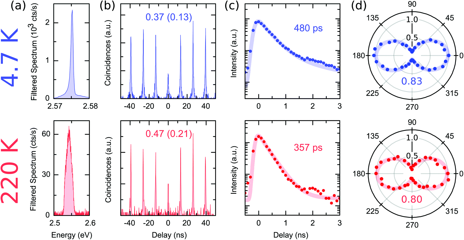 | ||
| Fig. 3 Experimental evidence of fast polarisation-controlled single photon emission at both 4.7 (upper) and 220 K (lower). (a) Filtered μ-PL spectra, with which the HBT, time-resolved, and polarisation-resolved μ-PL measurements were made. The energy scale has been increased by a factor of 10 for the plot at 220 K. (b) Photon autocorrelation data, with both raw and background-corrected (in brackets) g(2)(0) values demonstrating single photon emission. (c) Time-resolved PL intensity plots of QD signals from which the exciton decay constant is extracted. For greater accuracy, the fitted curves are exponential decay functions convolved with the near-Gaussian instrument response function. (d) Emission intensity variation with polariser angle. A Malus’ Law type sinusoidal fitting has been used to demonstrate that the emission is polarised, with the same polarisation axis at both low and high temperatures. | ||
At 4.7 and 220 K, we measure raw g(2)(0) values of 0.37 and 0.47 respectively (Fig. 3(b)), thus confirming the single photon nature of the emission from the a-plane InGaN QD. Moreover, unlike other non-nitride single photon systems such as ref. 28, the g(2)(0) values are insensitive to temperature changes, and only increased slightly at 220 K. This could be attributed to the high exciton binding energies and large band offsets in III-nitride systems,30 which allow the QD emission to remain strong relative to the spectrally overlapping background QW emission as temperature increases. For this reason, we have also observed fast anti-bunching behaviour of this QD at 250 K (see ESI Fig. S1–S3†).
Non-zero raw g(2)(0) values are expected given the presence of spectrally overlapping background QW emission, as the QDs were formed on top of fragmented QWs during growth. Despite the aforementioned spectral selection, QW emission in the same wavelength window as the QD will also reach the single photon detectors. Since single photon emission only originates from the QD, light of the selected wavelength from any other source present will increase the g(2)(0) values. To understand the g(2)(0) values expected from the QD alone, a commonly used background reduction calculation is performed. This background reduction can be accounted for using ρ, the ratio of QD intensity to the total intensity recorded by the photomultiplier tubes (PMTs), and the correction formula,44
 | (4) |
The ρ was estimated to be 85% at 4.7 K, and 82% at 220 K. The estimation method is explained in the ESI (Fig. S1†). Calculations with eqn (4) yield g(2)corr(0) values of 0.13 and 0.21 respectively (cf.Fig. 3(b)). These values are much closer to 0, indicating that the QD is behaving as a single photon emitter in the presence of a weak QW background. As we use non-resonant excitation, rapid re-population and re-emission30 from the QDs could be reasons for the occasional emission of more than one photon. Moreover, the difficulty in obtaining highly accurate estimates of ρ should still be a significant reason that the g(2)corr(0) values are not closer to 0.
The characteristic radiative lifetime of the QD has been assessed by performing time-resolved μ-PL. The resulting decay plots at 4.7 and 220 K can be seen in Fig. 3(c). Fitting of this lifetime data has been performed using a modified Gaussian function as shown in eqn (5),
| f(t) = f0 + (fGauss⊗fexp)(t), | (5) |
Lastly, the polarisation properties of the QD emission have been analysed by polarisation-resolved μ-PL. Our previous investigations37 have shown that the emission from an a-plane InGaN QD not only has a statistically high average degree of optical linear polarisation (DOLP) of 0.90 ± 0.08, but also possesses an intrinsic axis of polarisation along the crystal m-direction. PL intensities of the studied QD at different polariser angles at both 4.7 and 220 K have been recorded and analysed. As shown in Fig. 3(d), the sinusoidal fits in accordance with Malus’ Law show that the emission is polarised at both temperatures. The maximum and minimum intensities recorded, Imax and Imin, were used to calculate the polarisation degree with eqn (6),
 | (6) |
DOLP values of 0.83 ± 0.01 and 0.80 ± 0.13 have been obtained for 4.7 and 220 K respectively, indicating highly polarised single photon emission at both low and high temperatures. The use of a-plane QDs breaks the nitride wurtzite symmetry and lowers it to orthorhombic, leading to hole state splitting and band mixing effects. The resultant exciton hole ground state has a much higher contribution from the state associated with emission along the m-direction than the c-direction, yielding not only high DOLPs, but also a deterministic polarisation axis.37 Indeed, the axis of polarisation for all QDs observed lies along the m-direction of the sample. As such, the direction of polarisation for these polarised single photon emitters is predefined by the material crystallography, a simpler and more efficient approach than attempting to use strain engineering for polarisation control, or using an external polariser. After sample preparation, striations are visible along the sample surface, arising from the growth process, and are aligned perpendicular to the m-direction, making the identification of the polarisation axis straightforward in our experiments. The DOLP at 220 K indicates that the QD exciton transition has similarly high |m〉-like characteristics at elevated temperatures, thereby confirming the ability of a-plane InGaN QDs to operate as single photon sources with polarisation control in on-chip temperature regimes.
Conclusions
In summary, we have demonstrated simultaneous single photon generation, polarised light emission with a predefined polarisation axis, a fast GHz repetition rate, and operation at 220 K, above the thermoelectric cooling barrier, promising in-principle operability in the conditions of integrated electronic systems. The radiative lifetime, polarisation degree and orientation, and g(2)(0) are all temperature insensitive. At the current stage, work still needs to be done to reduce the background QW emission for purer single photon emission, and to improve fabrication quality for higher brightness, narrower linewidth, and slower thermal quenching of emission intensity. However, as an initial demonstration, the results in this work show that without resorting to material defects or complex device geometries, polarisation-controlled single photon generation can be realised in solid-state QDs beyond the Peltier cooling threshold. The a-plane InGaN system described here is hence a good candidate for the further development of polarised single photon sources operable at on-chip conditions.Experimental
Sample preparation
Non-polar (11−20) InGaN QDs were grown by a modified droplet epitaxy method as described previously.34,47 InGaN QDs were positioned in the centre of a 50 nm thick intrinsic GaN layer, which was clad by 600 nm of n-doped GaN and 200 nm of p-doped GaN. Based on the analysis of atomic force microscopy images of an uncapped InGaN QD sample, the QDs have an average height of ∼7 nm, diameter of ∼35 nm, and a density of approximately 1 × 109 cm−2. To isolate individual QDs, we processed the as-grown wafer into nanopillar structures by drop-casting of silica nanospheres onto the wafer as an etch mask, followed by dry etching to a depth of ∼350 nm. The residual silica nanosphere etch mask was then removed by ultra-sonication and a buffered-oxide etch. Details of the p–i–n sample growth and nanopillar processing conditions can be found in ref. 37. Such nanopillar structures provide better collimation and directionality for the emitted photon, thus higher photon extraction efficiency.Optical characterisation
μ-PL experiments were performed with the sample mounted on a nano-positioning system (∼nm precision Attocube positioners) contained in a close-cycle cryostat (AttoDRY 800), varying the sample temperature between 4.7 and 320 K. Excitation was provided using a mode-locked Ti:Sapphire laser operating at a wavelength of 800 nm (pulse duration ∼1 ps, repetition rate ∼76 MHz). The wavelength of 800 nm was chosen to allow 2-photon excitation of the sample, as QDs have a larger relative absorption cross-section for multi-photon processes than QWs, and hence the QD![[thin space (1/6-em)]](https://www.rsc.org/images/entities/char_2009.gif) :QW (signal:background) ratio is improved.48
:QW (signal:background) ratio is improved.48
The excitation laser was focused onto the sample through an objective lens (100×, 0.5 N.A.), with sample emission collected back through the same objective. Spectra are assessed using a 0.5 m focal length spectrometer (1200 l mm−1 grating). HBT experiments were performed by spectrally isolating the QD using a pair of tuneable bandpass filters and passing the filtered signal through a 50:50 beam-splitter connected to two PMTs. Signals from these PMTs are time-tagged using a time-correlated single photon counting module with up to 25 ps time resolution. The PMTs define start and stop times individually. Similarly, lifetime data is collected by passing the spectrally filtered emission from the sample to a single PMT and using a fast-photomultiplier at the excitation laser as the start timer of the time-correlated single photon counting module.
Polarisation measurements were performed by introducing a linear polariser and half-wave plate into the optical collection arm of the μ-PL system, with the transmission axis (0° marking) aligned to the PL component parallel to the [1−100] m-axis of the sample. The half-wave plate was used in order to maintain the same polarisation axis for light entering the spectrograph, in order to negate any polarisation dependent effects in the detection system itself.
Author Contributions
‡T. W. and T. J. P. contributed equally to this work. T. J. P. devised the optical setup, and T. W. conducted the optical experiments. T. W. and T. J. P. analysed the data together. T. Z. devised the crystal growth method and grew and characterised the material, and, with J. C. J, fabricated the nanopillar structures. L. P. N. designed computer programmes to facilitate the HBT experiments. R. A. O. supervised the sample growth and processing, and R. A. T. supervised the optical characterisation.Acknowledgements
This research was supported by the UK Engineering and Physical Sciences Research Council (EPSRC) Grants EP/M012379/1 and EP/M011682/1. T. W. is grateful for the award of the National Science Scholarship (NSS) as PhD funding by the Singapore Agency for Science, Technology and Research (A*STAR). R. A. O. is grateful to the Royal Academy of Engineering and the Leverhulme Trust for a Senior Research Fellowship.References
- I. Aharonovich, D. Englund and M. Toth, Nat. Photonics, 2016, 10, 631–641 CrossRef CAS.
- B. Lounis and W. E. Moerner, Nature, 2000, 407, 491–493 CrossRef CAS PubMed.
- T. T. Tran, K. Bray, M. J. Ford, M. Toth and I. Aharonovich, Nat. Nanotechnol., 2016, 11, 37–41 CrossRef CAS PubMed.
- M. Kianinia, S. A. Tawfik, B. Regan, T. T. Tran, M. J. Ford, I. Aharonovich and M. Toth, ACS Photonics, 2017, 4, 768–773 CrossRef CAS.
- N. Mizuochi, T. Makino, H. Kato, D. Takeuchi, M. Ogura, H. Okushi, M. Nothaft, P. Neumann, A. Gali, F. Jelezko, J. Wrachtrup and S. Yamasaki, Nat. Photonics, 2012, 6, 299–303 CrossRef CAS.
- S. Castelletto, B. C. Johnson, V. Ivády, N. Stavrias, T. Umeda, A. Gali and T. Ohshima, Nat. Mater., 2013, 13, 151–156 CrossRef PubMed.
- A. J. Morfa, B. C. Gibson, M. Karg, T. J. Karle, A. D. Greentree, P. Mulvaney and S. Tomljenovic-Hanic, Nano Lett., 2012, 12, 949–954 CrossRef CAS PubMed.
- A. M. Berhane, K. Jeong, Z. Bodrog, S. Fiedler, T. Schröder, N. V. Triviño, T. Palacios, A. Gali, M. Toth, D. Englund and I. Aharonovich, Adv. Mater., 2017, 29, 1605092 CrossRef PubMed.
- X. Ding, Y. He, Z. C. Duan, N. Gregersen, M. C. Chen, S. Unsleber, S. Maier, C. Schneider, M. Kamp, S. Höfling, C. Y. Lu and J. W. Pan, Phys. Rev. Lett., 2016, 116, 020401 CrossRef PubMed.
- N. Somaschi, V. Giesz, L. De Santis, J. C. Loredo, M. P. Almeida, G. Hornecker, S. L. Portalupi, T. Grange, C. Anton, J. Demory, C. Gomez, I. Sagnes, N. D. L. Kimura, A. Lemaitre, A. Auffeves, A. G. White, L. Lanco and P. Senellart, Nat. Photonics, 2016, 10, 340–345 CrossRef CAS.
- J. Claudon, J. Bleuse, N. S. Malik, M. Bazin, P. Jaffrennou, N. Gregersen, C. Sauvan, P. Lalanne and J.-M. Gérard, Nat. Photonics, 2010, 4, 174–177 CAS.
- K. H. Madsen, S. Ates, J. Liu, A. Javadi, S. M. Albrecht, I. Yeo, S. Stobbe and P. Lodahl, Phys. Rev. B: Condens. Matter, 2014, 90, 155303 CrossRef.
- S. Deshpande, A. Das and P. Bhattacharya, Appl. Phys. Lett., 2013, 102, 161114 CrossRef.
- S. Deshpande, T. Frost, A. Hazari and P. Bhattacharya, Appl. Phys. Lett., 2014, 105, 141109 CrossRef.
- P. Bhattacharya, S. Deshpande, T. Frost and A. Hazari, Proc. SPIE-Int. Soc. Opt. Eng., 2015, 9382, 938207 CrossRef.
- C. H. Teng, L. Zhang, T. A. Hill, B. Demory, H. Deng and P. C. Ku, Appl. Phys. Lett., 2015, 107, 191105 CrossRef.
- J.-H. Kim, Y.-H. Ko, S.-H. Gong, S.-M. Ko and Y.-H. Cho, Sci. Rep., 2013, 3, 2150 CrossRef PubMed.
- S. Deshpande, J. Heo, A. Das and P. Bhattacharya, Nat. Commun., 2013, 4, 1675 CrossRef PubMed.
- A. Lundskog, C.-W. Hsu, K. Fredrik Karlsson, S. Amloy, D. Nilsson, U. Forsberg, P. Olof Holtz and E. Janzén, Light: Sci. Appl., 2014, 3, e139 CrossRef CAS.
- T. Jemsson, H. Machhadani, P.-O. Holtz and K. F. Karlsson, Nanotechnology, 2015, 26, 65702 CrossRef CAS PubMed.
- L. Zhang, C. H. Teng, P. C. Ku and H. Deng, Appl. Phys. Lett., 2016, 108, 153102 CrossRef.
- T. J. Puchtler, T. Wang, C. X. Ren, F. Tang, R. A. Oliver, R. A. Taylor and T. Zhu, Nano Lett., 2016, 16, 7779–7785 CrossRef CAS PubMed.
- M. J. Holmes, S. Kako, K. Choi, M. Arita and Y. Arakawa, Proc. SPIE-Int. Soc. Opt. Eng., 2016, 9748, 97481E CrossRef.
- Ž. Gačević, M. Holmes, E. Chernysheva, M. Müller, A. Torres-Pardo, P. Veit, F. Bertram, J. Christen, J. M. González Calbet, Y. Arakawa, E. Calleja and S. Lazić, ACS Photonics, 2017, 4, 657–664 CrossRef.
- C. H. Bennett and G. Brassard, in Proceedings of IEEE International Conference on Computers, Systems, and Signal Processing, 1984, pp. 175–179.
- D. Loss and D. P. DiVincenzo, Phys. Rev. A, 1998, 57, 120–126 CrossRef CAS.
- O. Fedorych, C. Kruse, A. Ruban, D. Hommel, G. Bacher and T. Kümmell, Appl. Phys. Lett., 2012, 100, 061114 CrossRef.
- S. Bounouar, M. Elouneg-Jamroz, M. Den Hertog, C. Morchutt, E. Bellet-Amalric, R. André, C. Bougerol, Y. Genuist, J. P. Poizat, S. Tatarenko and K. Kheng, Nano Lett., 2012, 12, 2977–2981 CrossRef CAS PubMed.
- S. Kako, C. Santori, K. Hoshino, S. Götzinger, Y. Yamamoto and Y. Arakawa, Nat. Mater., 2006, 5, 887–892 CrossRef CAS PubMed.
- M. J. Holmes, K. Choi, S. Kako, M. Arita and Y. Arakawa, Nano Lett., 2014, 14, 982–986 CrossRef CAS PubMed.
- M. J. Holmes, S. Kako, K. Choi, M. Arita and Y. Arakawa, ACS Photonics, 2016, 3, 543–546 CrossRef CAS.
- R. Bardoux, T. Guillet, B. Gil, P. Lefebvre, T. Bretagnon, T. Taliercio, S. Rousset and F. Semond, Phys. Rev. B: Condens. Matter, 2008, 77, 235315 CrossRef.
- R. H. Hadfield, Nat. Photonics, 2009, 3, 696–705 CrossRef CAS.
- T. Zhu, F. Oehler, B. P. L. Reid, R. M. Emery, R. A. Taylor, M. J. Kappers and R. A. Oliver, Appl. Phys. Lett., 2013, 102, 251905 CrossRef.
- S. K. Patra, T. Wang, T. J. Puchtler, T. Zhu, R. A. Oliver, R. A. Taylor and S. Schulz, Phys. Status Solidi B, 2017 DOI:10.1002/pssb.201600675.
- B. P. L. Reid, T. Zhu, C. C. S. Chan, C. Kocher, F. Oehler, R. Emery, M. J. Kappers, R. A. Oliver and R. A. Taylor, Phys. Status Solidi C, 2014, 11, 702–705 CrossRef CAS.
- T. Wang, T. J. Puchtler, S. K. Patra, T. Zhu, M. Ali, T. Badcock, T. Ding, R. A. Oliver and R. A. Taylor, 2016, arXiv:1609.06885, https://arxiv.org/abs/1609.06885.
- A. M. Jagtap, J. Khatei and K. S. Koteswara Rao, Phys. Chem. Chem. Phys., 2015, 17, 27579 RSC.
- T. Braun, C. Schneider, S. Maier, R. Igusa, S. Iwamoto, A. Forchel, S. Hofling, Y. Arakawa and M. Kamp, AIP Adv., 2014, 4, 97128 CrossRef.
- R. Seguin, S. Rodt, A. Strittmatter, L. Reißmann, T. Bartel, A. Hoffmann, D. Bimberg, E. Hahn and D. Gerthsen, Appl. Phys. Lett., 2004, 84, 4023 CrossRef CAS.
- S. A. Empedocles and M. G. Bawendi, J. Phys. Chem. B, 1999, 103, 1826–1830 CrossRef CAS.
- K. Sebald, H. Lohmeyer, J. Gutowski, T. Yamaguchi and D. Hommel, Phys. Status Solidi B, 2006, 243, 1661–1664 CrossRef CAS.
- S. Buckley, K. Rivoire and J. Vučković, Rep. Prog. Phys., 2012, 75, 126503 CrossRef PubMed.
- R. Brouri, A. Beveratos, J.-P. Poizat and P. Grangier, Opt. Lett., 2000, 25, 1294 CrossRef CAS PubMed.
- M. Holmes, S. Kako, K. Choi, M. Arita and Y. Arakawa, Phys. Rev. B: Condens. Matter, 2015, 92, 115447 CrossRef.
- S. Kako, M. Holmes, S. Sergent, M. Bürger, D. J. As and Y. Arakawa, Appl. Phys. Lett., 2014, 104, 11101 CrossRef.
- T. Wang, T. J. Puchtler, T. Zhu, J. C. Jarman, R. A. Oliver and R. A. Taylor, Phys. Status Solidi B, 2017 DOI:10.1002/pssb.201600724.
- A. F. Jarjour, A. M. Green, T. J. Parker, R. A. Taylor, R. A. Oliver, G. Andrew, D. Briggs, M. J. Kappers, C. J. Humphreys, R. W. Martin and I. M. Watson, Physica E, 2006, 32, 119–122 CrossRef CAS.
Footnotes |
| † Electronic supplementary information (ESI) available: Fast, antibunched emission up to 250 K. See DOI: 10.1039/c7nr03391e. All numerical data in the figures are available at DOI: 10.5287/bodleian:4r7JoNnr2 |
| ‡ These authors contributed equally to this work. |
| This journal is © The Royal Society of Chemistry 2017 |