
 Open Access Article
 This Open Access Article is licensed under a Creative Commons Attribution-Non Commercial 3.0 Unported Licence
High surface coverage of a self-assembled monolayer by in situ synthesis of palladium nanodeposits†
Lucía
Herrer
abc,
Victor
Sebastian
 *ade,
Santiago
Martín
cf,
Alejandro
González-Orive
abc,
Francesc
Pérez-Murano
g,
Paul J.
Low
h,
José Luis
Serrano
ai,
Jesús
Santamaría
ade and
Pilar
Cea
*abc
*ade,
Santiago
Martín
cf,
Alejandro
González-Orive
abc,
Francesc
Pérez-Murano
g,
Paul J.
Low
h,
José Luis
Serrano
ai,
Jesús
Santamaría
ade and
Pilar
Cea
*abc
aInstituto de Nanociencia de Aragón (INA), Campus Río Ebro, Universidad de Zaragoza, C/Mariano Esquillor, s/n, 50018 Zaragoza, Spain. E-mail: victorse@unizar.es; pilarcea@unizar.es
bLaboratorio de Microscopias Avanzadas (LMA), Campus Río Ebro, Universidad de Zaragoza, C/Mariano Esquilor, s/n, 50018 Zaragoza, Spain
cDepartamento de Química Física, Facultad de Ciencias, Universidad de Zaragoza, 50009, Zaragoza, Spain
dNetworking Biomedical Research Center of Bioengineering, Biomaterials and Nanomedicine (CIBER-BBN), C/ Monforte de Lemos 3-5, Pabellón 11, 28029 Madrid, Spain
eDepartamento de Ingeniería Química y Tecnología del Medio Ambiente, Universidad de Zaragoza, C/Mariano Esquilor, s/n, 50018 Zaragoza, Spain
fInstituto de Ciencia de Materiales de Aragón (ICMA), Universidad de Zaragoza-CSIC, 50009 Zaragoza, Spain
gInstituto de Microelectrónica de Barcelona (IMB-CNM, CSIC), Campus UAB, 08193 Bellaterra, Spain
hSchool of Molecular Sciences, University of Western Australia, 35 Stirling Highway, Crawley, Perth 6009, Australia
iDepartamento de Química Orgánica, Facultad de Ciencias, Universidad de Zaragoza, 50009, Zaragoza, Spain
First published on 10th August 2017
Abstract
Nascent metal|monolayer|metal devices have been fabricated by depositing palladium, produced through a CO-confined growth method, onto a self-assembled monolayer of an amine-terminated oligo(phenylene ethynylene) derivative on a gold bottom electrode. The high surface area coverage (85%) of the organic monolayer by densely packed palladium particles was confirmed by X-ray photoemission spectroscopy (XPS) and atomic force microscopy (AFM). The electrical properties of these nascent Au|monolayer|Pd assemblies were determined from the I–V curves recorded with a conductive-AFM using the Peak Force Tunneling AFM (PF-TUNA™) mode. The I–V curves together with the electrochemical experiments performed rule out the formation of short-circuits due to palladium penetration through the monolayer, suggesting that the palladium deposition strategy is an effective method for the fabrication of molecular junctions without damaging the organic layer.
Introduction
Molecular electronics is a dynamic field of contemporary research with enormous potential to approach not only concerns over ‘top-down’ scaling of electronic components, but also identify a wide range of technological and scientific challenges that are reliant on electron-transfer between molecular systems and solid-state interfaces including solar-energy harvesting, thermoelectric materials, catalysis, and sensing.1 Significant progress has been made in the last few years including the synthesis of new functional molecular materials,2–10 development of sophisticated methods for the assembly of either single molecules or monolayers onto electrodes for the achievement of efficient molecule–electrode junctions,11–15 as well as experimental methods to determine the electrical properties of molecules at a single level16–22 or in monolayers.23,24 However, several challenges remain to be addressed before molecular electronics turns into a truly viable and reliable technology.25 The fabrication of the top contact electrode in two terminal sandwich-based metal|organic monolayer|metal devices is one of the major challenges that, despite intense research over more than 30 years, remains to be fully resolved.15,26–30 A wide variety of techniques to deposit the top metal electrode onto a molecular monolayer have been described in the literature including direct and indirect evaporation,11,31–38 use of liquid metals,11,34,39,40 flip chip lamination,34,41 electrodeposition,42–44 surface-diffusion-mediated deposition,44 chemisorption of metal nanoparticles onto surface-functionalised monolayers,45 thermal induced decomposition of an organometallic monolayer,46 and photoreduction of a metal precursor.47,48 The most significant problems in the deposition of the top-contact electrode are those related to damage of the functional molecules during the metallization process of the monolayer or penetration of the growing top-contact through the monolayer, which results in short circuits. In addition, many of the proposed ‘soft’ methods that avoid penetration of the growing metal electrode through the monolayer result in a relatively low surface coverage of the monolayer by the newly fashioned top contact.45–47In this contribution, a simple procedure for the deposition of a metallic top-contact electrode onto a monolayer film of ‘wire-like’ molecules is presented. A self-assembled monolayer (SAM) of an oligo(phenylene ethynylene) (OPE) derivative, 4-(2-(4-(2-(4-aminophenyl)ethynyl)phenyl)ethynyl)benzenamine, 1, featuring amine functional groups to provide metallic contacts49,50 has been used as the wire-like molecular component. This allows benchmarking of the electrical performance against similar device structures and helps assess the effectiveness of this top-contact deposition method (Fig. 1). Anisotropic palladium nanostructures were initially produced with the assistance of a CO-confined growth method.51,52 Carbon monoxide molecules, which strongly adsorb onto the basal (111) planes of palladium nanosheets, are used to block the growth of the metallic particle along the [111] direction and direct the formation of sheet-like structures.51 These metallic palladium sheets are aggregated onto the monolayer to generate larger palladium nanodeposits (PdND) across the surface. This method results in a larger surface coverage of palladium than that previously achieved with gold45,47 or silver53 by the assembly of metal nanoparticles onto organic monolayers.
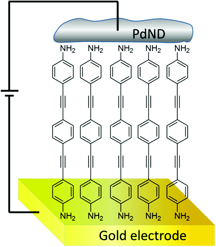 | ||
| Fig. 1 Structure of the gold|SAM(1)|PdND devices presented in this paper. | ||
Experimental
Compound 1 was synthesized as described elsewhere.54 Gold substrates were purchased from Arrandee®, Schroeer, Germany, and flame-annealed at approximately 800–1000 °C with a Bunsen burner immediately prior to use. This procedure is known to result in atomically flat Au(111) terraces.55 Self-assembled monolayers (SAMs) were prepared by immersion of the annealed gold-on-glass substrates in a 10−4 M solution of 1 in tetrahydrofuran (THF, HPLC grade ≥99.9%, inhibitor-free solution) for 48 hours. Afterwards, the surface-modified substrates (denoted gold|SAM(1)) were thoroughly rinsed with THF and dried under a stream of dry nitrogen.A stainless steel, Teflon lined autoclave (Fig. 2a) was fitted with a specially designed Teflon insert to create two compartments (termed mixing and growth chambers), connected by lateral windows (Fig. 2b). The monolayer-modified gold substrate (i.e. gold|SAM(1)) was attached face down within the lower growth chamber to prevent deposition of particulate matter by gravity (Fig. 2c). A palladium growth solution was prepared by mixing 11 mg of sodium palladium(II) chloride (Na2PdCl4, Aldrich) and 130 mg of potassium bromide (KBr, Aldrich) in Milli-Q water (400 μL). The resulting red-coloured, homogeneous solution was mixed with 4 mL of dimethylformamide (DMF, EMD chemicals, used as received) and introduced into the autoclave. The solution was gently stirred with a magnetic flea located at the mixing chamber, whilst the lateral windows carved in the Teflon holder assured a good fluid transfer between the mixing chamber and the growth chamber (Fig. 2), reducing the presence of any concentration profiles that could affect the homogeneity and the surface coverage of the substrate. The autoclave was flushed under CO and pressurized to 6 bar, and the reactor heated at 80 °C for 50 min. Palladium nanodeposits are formed on the gold|SAM(1) resulting in sandwich structures denoted gold|SAM(1)|PdNDs.
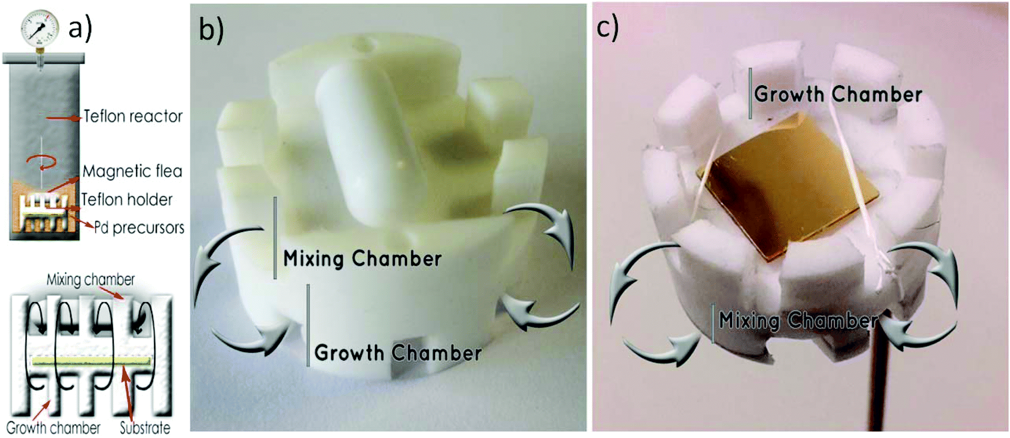 | ||
| Fig. 2 (a) Teflon holder designed to grow PdNDs onto organic monolayers. (b) Location of mixing and growth chambers with the fluid transfer between chambers by the lateral windows. (c) The gold|SAM(1) secured in the growth chamber; when the Teflon holder is placed in the autoclave, the exposed gold|SAM(1) surface is facing ‘down’ to limit adventitious deposition of PdNDs by gravity. | ||
X-ray photoelectron spectra (XPS) were recorded on a Kratos AXIS ultra DLD spectrometer with a monochromatic Al Kα X-ray source (1486.6 eV) using a pass energy of 20 eV. To provide a precise energy calibration, the XPS binding energies were referenced to the C 1s peak at 284.6 eV. The thickness of the SAM onto the gold substrate was estimated using the attenuation of the Au 4f signal from the substrate according to ISAM = Isubstrate![[thin space (1/6-em)]](https://www.rsc.org/images/entities/char_2009.gif) exp(−d/λsinθ), where d is the film thickness, ISAM and Isubstrate are the average of the intensities of the Au 4f5/2 and Au 4f7/2 peaks attenuated by the SAM and from bare gold, respectively; θ is the photoelectron take-off angle; and λ is the effective attenuation length of the photoelectron (4.2 ± 0.1 nm).56
exp(−d/λsinθ), where d is the film thickness, ISAM and Isubstrate are the average of the intensities of the Au 4f5/2 and Au 4f7/2 peaks attenuated by the SAM and from bare gold, respectively; θ is the photoelectron take-off angle; and λ is the effective attenuation length of the photoelectron (4.2 ± 0.1 nm).56
AFM images were obtained in tapping and peak-force modes using a Multimode 8 microscope equipped with a Nanoscope V control unit from Bruker operating under ambient air conditions at a scan rate of 0.5–1.2 Hz. To this end, RFESPA-75 (75–100 kHz, and 1.5–6 N m−1, nominal radius of 8 nm) and ScanAsyst-Air-HR tips (130–160 kHz, and 0.4–0.6 N m−1, nominal radius of 2 nm), purchased from Bruker, were used. In order to minimize tip convolution effects affecting the measurement of the width of the palladium nanodeposits, data obtained from AFM image profiling have been corrected according to Canet-Ferrer et al.57 The RMS (root mean square) roughness as well as bearing and depth statistical analyses were carried out by means of Nanoscope off-line v. 1.40 and Gwyddion v. 2.41 package software. The electrical properties of the molecular junctions were determined with a conductive-AFM (Bruker ICON) under humidity control, ca. 40%, with a N2 flow using the Peak Force Tunnelling AFM (PF-TUNA™) mode, and employing a PF-TUNA™ cantilever from Bruker (coated with Pt/Ir 20 nm, ca. 25 nm radius, 0.4 N m−1 spring constant and 70 kHz resonance frequency).
Cyclic voltammetry (CV) experiments were performed using a potentiostat from EcoChemie and a standard three-electrode cell, where the working electrode was a bare Au(111) electrode, an Au(111) electrode covered by a monolayer of 1, or an Au(111) electrode covered by a monolayer of 1 with palladium nanodeposits on top of the organic film. These working electrodes were connected to the potentiostat by means of a cable ended in a metallic tweezer that holds the electrode. The reference electrode was Ag/AgCl, KCl (3 M) and the counter electrode was a Pt sheet.
Results and discussion
The fabrication of the monolayer sandwich-style structures commenced with the initial deposition of high-quality self-assembled monolayers of 1 on flame-annealed gold-on-glass substrates offering large area (111) terraces. After the incubation of the gold substrate in a solution of compound 1 in a 10−4 M solution for 48 h, AFM imaging confirmed the formation of a homogenous and tightly packed organic layer with low occurrence of defects, pinholes, and three-dimensional aggregates (Fig. 3a). The characteristic features of the underlying Au(111) surface still remain detectable beneath the well-ordered monolayer, i.e. smooth terraces and monoatomic gold steps. Such a defect-free and densely packed organic monolayer is expected to contribute to avoid penetration of the top-contact electrode through the monolayer. By scratching the surface with the AFM tip, the average thickness of the film, namely 1.78 ± 0.14 nm, can be accurately estimated by carrying out height/depth profiles across the scratched area (Fig. S1 in the ESI†).57 This thickness is also in good agreement with the one determined from the attenuation of the Au 4f signal from the gold substrate in the XPS spectrum (see Fig. S2 in the ESI†), namely (1.85 ± 0.05 nm). The experimental thickness of the SAM of 1, as determined by any of the two experimental methods used, is in good agreement with the length of compound 1 (1.9 nm) determined from computational molecular models (Spartan®08 V1.0.0), suggesting an arrangement of 1 in the monolayer with a tilt angle of ca. 70° to the substrate surface. | ||
| Fig. 3 Representative AFM images of (a) gold|SAM(1) and (b) gold|SAM(1)|PdNDs. | ||
It is well known that cyclic voltammetry can be used as an indirect method for evaluating the presence of pores or holes in organic films deposited onto electrodes.58,59 Fig. S2† shows the electrochemical response of a bare gold electrode as well as the response of the gold-substrate covered by a SAM of 1 introduced into a solution containing an electrochemical probe, K3[Fe(CN)6]. The complete blocking exhibited by the gold substrate covered by the SAM of 1 within the potential window considered for the reversible diffusion-controlled redox probe is indicative of a tightly-packed film.60 Further relevant results are discussed in more detail below.
The mechanisms of nucleation and growth of nanoparticles in solution have been widely explored and described in detail elsewhere by others.61–64 According to the traditional LaMer mechanism of nucleation and growth of nanoparticles, nucleation of nanoparticles can take place under either homogeneous and heterogeneous conditions. Homogeneous nucleation occurs when nuclei form uniformly throughout the parent phase, whereas, heterogeneous nucleation commences at structural in-homogeneities on a surface. Consequently, the growth kinetics and size of the resulting nanoparticles are usually different in homogeneous and heterogeneous nucleation processes. However, whilst nucleation processes may be faster at the heterogeneous interface, a diffusion limited process is usually responsible for directing the growth of nanoparticles on substrates, allowing a more controlled and regular growth with lower density of defects in the particle distribution.65
Previous studies have used organic capping agents to produce Pd nanoparticles with sheet-like morphology.51,52 However, for the purpose of this work, the presence of organic compounds over the metallic top-contact would interfere with the planned electrical measurements. Palladium nanostructures were therefore prepared here without the assistance of added capping agents, exploiting the presence of Br− anions and CO pressure, the key variables to control the anisotropic growth of Pd, and the metallic palladium top-contact electrode was grown on top of the monolayer in a heterogeneous fashion, further taking advantage of CO-confined growth of palladium nanoparticles.
The reduction of the palladium precursor was performed in aqueous DMF solution in a CO-pressurized autoclave. The CO has a dual role in the formation of PdNDs: (1) it is a facet-specific capping agent that promotes the formation of sheet morphology by the preferential binding to {111} planes of the growing Pd particle, leading to ultra-thin sheet like morphology; (2) CO is a reducing agent and assists in the chemical reduction of Pd2+ ions to metallic palladium. Reagent composition and synthesis conditions (CO pressure, time and temperature) were optimized to give coverage of the SAM by PdNDs.
Fig. S4a and S4b† show representative sheet-like nanoparticles collected in the autoclave after reaction. Energy-dispersive X-ray spectroscopy confirmed the presence of Pd in the nanosheets in the bulk solution (Fig. S4c and S4d†). The mean diameter of the Pd nanosheets dispersed in the bulk solution ranged between 21 and 28 nm, obtained from a mixture of triangular and hexagonal morphologies. Fig. S4e† shows the representative UV-Vis spectra of a colloidal suspension of the Pd nanosheets. The surface plasmon resonance (SPR) peak exhibited by the Pd nanosheets is in full agreement with the reported data of the Pd nanosheets with similar dimensions.51,52 The robustness of the synthesis method is confirmed by the excellent reproducibility of the optical properties of the colloidal suspensions obtained from multiple independent syntheses (Fig. S4e†).
When the gold|SAM(1) system is placed in the reactor chamber, heterogeneous CO-controlled growth leads to Pd nanostructures that almost completely cover the SAM surface, with low occurrence of large 3D-aggregates (Fig. 3b). The resulting sandwich-like structures are denoted as gold|SAM(1)|PdNDs. The surface roughness, expressed in terms of the Root Mean Square (RMS), of the gold|SAM(1)|PdND assembly (2.64 ± 0.25 nm) is significantly greater than that of the gold|SAM(1) precursor structures (0.49 ± 0.09 nm) (Fig. S5†). The statistical analysis of the data provided by the AFM images indicates that the aggregated PdNDs are essentially disk-shaped with an average diameter (corrected by the tip convolution) of 15.7 ± 2.4 nm and an average height of 7.3 ± 1.5 nm (Fig. S6†). More importantly, the AFM images exhibit a remarkably high surface coverage of the SAM with heterogeneously grown PdNDs (Fig. 3b). A bearing analysis of the recorded AFM images was carried out in order to estimate the percentage of the SAM of 1 covered by the PdNDs (Fig. S7†). Such an analysis provides an accurate assessment of the image area covered by features with larger heights than the selected depth threshold66,67 and rendered an average PdND coverage of 84.5 ± 2.8% for the optimum conditions employed. A similar surface coverage area has been obtained from the SEM images of the gold|SAM(1)|PdND system (Fig. S8†). In comparison with analogous experiments carried out with other metallic nanoparticles self-assembled as a top-contact onto an aromatic-moiety monolayer, such as gold nanoparticles with a coverage of 25%46 and, more recently, with silver nanoparticles, 76%,53 a significant improvement in the surface coverage has been achieved by the CO-controlled growth method of palladium deposition. In light of the previous remarks, the shape and size of the palladium particles produced by CO-confined growth in solution by homogeneous nucleation does not necessarily map directly to the morphology of the metallic material grown under the same conditions but arising from heterogeneous nucleation on top of the SAM of 1. It is also worth mentioning that the incubation of a gold|SAM(1) into a bulk dispersion containing pre-formed Pd nanosheets (i.e. overnight incubation of the gold|SAM(1) substrate in a colloidal suspension of pre-formed Pd nanosheets prepared under the same CO-controlled growth conditions) results in a rather low surface coverage, ca. 5% (Fig. S9†). This result supports the importance of the heterogeneous growth model to the structures grown on the gold|SAM(1) substrates in the autoclave.
Deposition of metallic palladium nanodeposits on the SAM of 1 to give the gold|SAM(1)|PdND assembly has been further demonstrated by XPS (Fig. 4). The XPS spectrum shows four peaks, two at 333.7 and 351.8 eV originating from the gold substrate, and other two peaks at 334.2 and 339.5 eV, with an area ratio of 3:2 and a peak separation of 5.3 eV, which are associated with the (3d5/2) and (3d3/2) peaks of metallic palladium.68–70
 | ||
| Fig. 4 XPS spectrum of gold|SAM(1)|PdNDs. The grey line shows the recorded spectrum and the blue and red lines show the deconvolution of the original spectrum to distinguish contributions from gold and palladium. | ||
At this point it is critical to verify that the metal-deposition strategy does not result in short-circuits by penetration of PdNDs through the SAM and this is an effective route towards the deposition of a top-contact electrode on a monolayer film. To do so, I–V curves were recorded for gold|SAM(1)|PdND structures using a conductive atomic force microscope (c-AFM) with the PeakForce tunneling AFM (PF-TUNA) mode and a PF-TUNA cantilever (coated with Pt/Ir 20 nm, ca. 25 nm radius, 0.4 N m−1 spring constant and 70 kHz resonance frequency).46,53,71–73 Under these conditions, the tip makes intermittent contact with the surface at a frequency of 2 kHz and a low maximum force (peak-force) to limit damage to the surface and detrimental lateral forces. Therefore, the peak-force tapping mode is useful for the conductivity mapping of soft or fragile samples, since lateral forces are avoided. Nevertheless, before recording the I–V curves, a compromise has to be made in order to select the most suitable contact force to be applied during the measurement since too much force results in unacceptably large deformation of the SAM underlying the PdNDs, while too little force yields an inadequate electrical contact between the AFM probe tip and the PdNDs. The deformation or damage of the monolayer has been investigated as a function of the tip loading force (set-point force) to help determine the most suitable set-point force for the subsequent electrical measurements (Fig. 5a). In the 1–8 nN set-point force range, the section analysis for three isolated PdNDs (inset Fig. 5a) shows practically constant heights (relative height determined with respect to the immediate surroundings of the PdNDs that may contain other PdNDs in the background) indicating that no significant deformation of the monolayer occurs and that the PdNDs are not substantially pushed into the monolayer by the AFM tip. If the set-point force is increased up to 12 nN, the section analysis of these PdNDs gives lower height values revealing deformation of the monolayer for this applied set-point force. If the set-point is increased to 15.5 nN the deformation of the monolayer increases with lower height values obtained from the section analysis. After applying a set-point force of 19.5 nN, two of these PdNDs are not visible indicating that these PdNDs have been pushed down into the relatively soft underlying monolayer by the pressure exerted from the AFM values, e.g. to 1 nN, the section analysis of these PdNDs is restored. Therefore, the deformation of the monolayer caused by applying a set-point force of 19.5 nN at the AFM tip is reversible and induces no apparent damage of the organic layer.
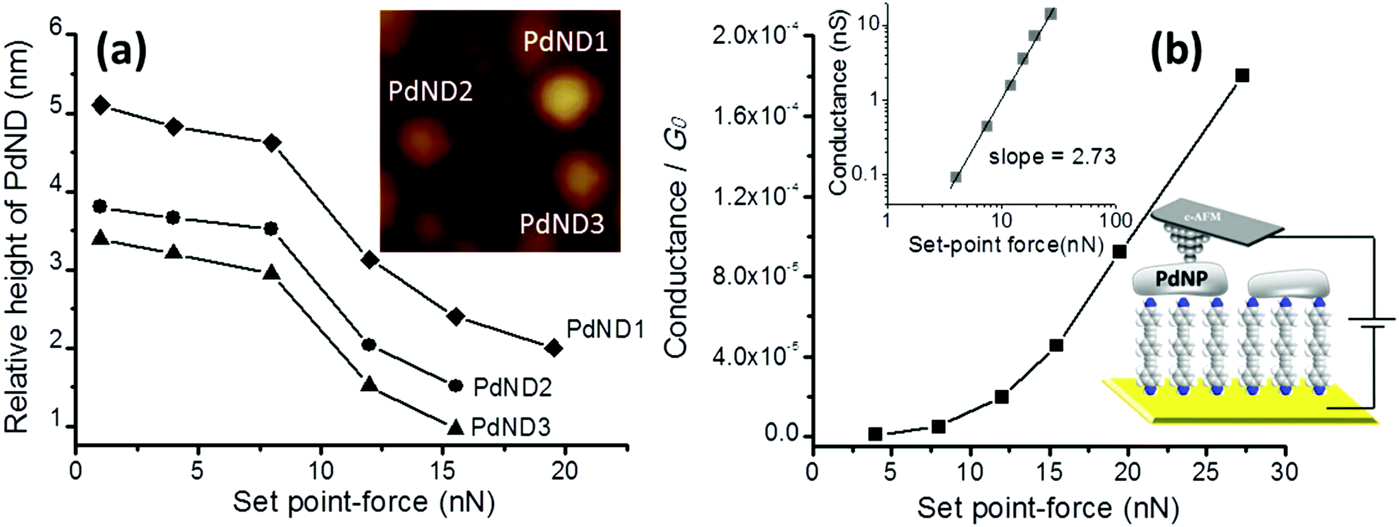 | ||
| Fig. 5 (a) Relative height of three PdNDs determined with the c-AFM at the indicated set-point forces. These PdNDs were used to study the deformation of the monolayer as a function of the set-point force. The inset shows a 150 × 150 nm2 image where the three PdNDs can be clearly distinguished; the Z range is 12 nm. (b) Conductance values measured locating the tip of the c-AFM onto a PdND vs. the applied set point-force (determined from the linear section (−0.5 to +0.5 V range) in the recorded I–V curve). Top inset figure: log–log plot to evidence the presence of a single power regime in the load force region explored in this work. Bottom inset figure: Cartoon showing the SAM onto a gold underlying electrode and the PdND contacted by the c-AFM tip. | ||
Turning to the electrical response, when a set-point force below 4 nN was used practically no current was detected, whilst for a set-point force between 4 and 8 nN a low conductance was obtained. These results suggest that when low set-point forces are applied, the contact between the tip and the PdND does not result in any measureable electrical current flow. Nevertheless, when a higher set-point force (between 12 and 27.3 nN) is applied, the I–V curves show a significant conductance, revealing that for these set-point forces there is a good electrical contact. In addition, top inset of Fig. 5b shows a log–log plot that evidence the increase in junction conductance versus the applied set-point force. In this case, a single power law regime74,75 (i.e., log(conductance) ∝ log (set-point force)·n where n = +2.73) can be observed for the set point force range explored in this work. In conclusion, a set-point force of 12 nN represents the minimum load required to make a reasonable contact between the tip and the PdND, minimizing any possible damage or excessive deformation of the organic layer during the determination of the electrical properties, although slightly higher loads do not show either evidence of a different power low regime or short-circuits.
Some 250 I–V curves were recorded by positioning the AFM tip on top of a PdND using a 12 nN set-point force, and by applying a bias between the underlying gold electrode and the tip (inset Fig. 5b). The individual I–V curves show a shape commonly observed for metal–molecule–metal junctions, with a linear section only at relatively low bias voltages (−0.5 to +0.5 V) and increasing curvature at higher bias (Fig. 6). Importantly, no low-resistance traces characteristic of metallic short circuits were observed in any of the individual I–V curves, which rules out the presence of short-circuits. The same behavior was also observed for I–V curves from gold|SAM(1)|PdND junctions collected at set-point forces of up to 27.3 nN (Fig. S10†). For simple monolayers of 1 on gold, i.e. without the PdND, a set point force of 8 nN was established as being sufficient to make good electrical contact without damage or excessive deformation to these softer surfaces. The I–V curves collected from these Pd free junctions also exhibit the typical shape associated with metal|molecule|metal junctions. This conformity of results from junctions comprised of SAM of 1 with and without PdNDs establish that the deposition process does not damage the underlying SAM, and does not alter or contaminate the interfaces.
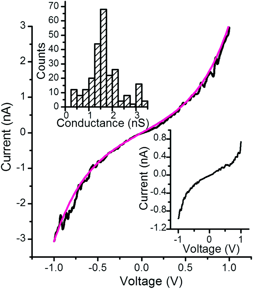 | ||
| Fig. 6 Representative I–V curve for a gold|SAM(1)|PdND system (black) obtained by positioning the c-AFM tip on top of a PdND and fitting according to the Simmons equation, Φ = 0.66 eV, α = 0.58 (magenta line). Inset top graph: Conductance histogram built from all the experimental data from −0.5 to 0.5 V for each I–V curve recorded (ca. 250 curves) positioning the tip onto a PdND and applying a set point-force of 12 nN. Inset bottom graph: Representative I–V curve for a gold-SAM device obtained by positioning the c-AFM tip directly onto the SAM and applying a set point-force of 8 nN. | ||
The representative I–V curve shown in Fig. 6 fits in good agreement with the Simmons model76 (where Φ is the effective barrier height of the tunneling junction relative to the Fermi level of the Au) and α is related to the effective mass of the tunneling electron. Φ and α are the fit parameters revealing that the mechanism of transport through these metal–molecule–metal junctions is non-resonant tunneling with an effective barrier height, Φ, of the tunneling junction of 0.66 eV, in excellent agreement with other similar OPE derivatives54,77–79 which also rules out the presence of short circuits since short circuits would result in lower values of Φ.
To further explore the steps in the fabrication process, the electrochemical (cyclic votammetric) response of the [Fe(CN)6]3−/[Fe(CN)6]4− couple at a bare Au(111) electrode, an Au(111) electrode modified by a SAM of 1, and an Au(111) electrode modified to give a gold|SAM(1)|PdND structure was examined (Fig. 7a). At the bare gold electrode, a well-defined, electrochemically reversible Fe(III/II) couple is readily observed. The complete inhibition of the electron transfer (ET) reaction to the [Fe(CN)6]3− redox probe observed for the SAM of 1 modified electrode together with the significant decrease in the capacitance in comparison with the bare Au(111) electrode is consistent with the formation of a tightly-packed monolayer that effectively blocks the diffusion of ions to the underlying gold electrode. From consideration of the size of the ferricyanide redox probe, it has been estimated that the complete inhibition of ET is achieved at a monolayer-modified electrode with pinholes below 0.5 nm diameter.80,81 Additionally, organic layers containing a nitrogen terminated-group are well known to favour considerably the on-top deposition of noble metal nanostructures (Au, Pt, Pd, etc.) with reference to the bare substrate by interacting strongly with the salt precursors.82–86 The diffusion of palladium or palladium precursors through the tightly packed SAM of 1 therefore appears be strongly hindered, which in turn is consistent with the lack of palladium penetration into the monolayer.
 | ||
| Fig. 7 (a) Cyclic voltammograms registered at 0.050 V s−1 in a 1 mM K3[Fe(CN)6] solution in 0.1 M KCl for the indicated working electrodes. (b) Cyclic voltammograms registered at 0.1 V s−1 in 0.1 M H2SO4 for the indicated electrodes. The reference electrode was in both cases Ag/AgCl, KCl (3 M). | ||
In contrast to the noticeable suppression of the Faradaic electrochemical response of the redox probe at the gold|SAM(1) electrode, once the PdNDs have been deposited onto the SAM of 1, a reversible voltammetric profile analogous to that exhibited by the bare gold electrode is obtained (Fig. 7a). This significant increase in the ET kinetics is indicative of a metallic-nanodeposit mediated ET through the passivated SAM of 1. This phenomenon, i.e. restoration of ET mediated by metallic nanoparticles, has been elegantly addressed by Chazalviel et al.87 and others82,88–90 and attributed to the fact that ET between two metallic phases separated by an organic layer under an applied bias voltage, is orders of magnitude faster, even with electrons tunnelling through the inner organic layer, than ET between a metal and a dilute redox species in solution.
It is also noteworthy that the gold|SAM(1)|PdND system results in a slightly larger ΔEp as well as a reduced current density of the peak in the voltammogram with respect to a bare gold electrode. It is well known that the ET properties exhibited by electrode/organic layer/metallic nanoparticle systems depend on the surface density of the top metallic deposit (the higher the surface density, the higher the current restoration),82,90,91 which is remarkably high in the gold|SAM(1)|PdND system described here. Additionally, the current density of electrode|organic layer|metallic nanoparticles also may depend on the thickness of the organic layer. Thus, it has been proven that the ET results are independent of the thickness of the organic film until a certain threshold is reached, after which the thicker the organic film is the slower is the rate of the ET.87,89 The transition from the transfer unaffected (full restoration of the current density after deposition of the top metal) to the transfer hindered regime is also dependent on the top metal nanoparticle size, with very small nanoparticles favoring a transfer hindered regime. Although for 16 nm diameter metallic nanoparticles the threshold monolayer thickness for the transition from ET thickness independent of the ET thickness dependent regime is predicted to be ca. 2.5 nm,87 the experimental results here presented indicate that a thickness of 1.8 nm for the SAM of 1 is enough to hamper slightly the ET as observed in Fig. 7a. This result is in agreement with previous observations such as that of Gooding and co-workers that obtained experimentally, for 27 nm gold nanoparticles, an organic film thickness threshold of 2.0 nm, which compares with the predicted value of 2.8 nm.89
The electrochemical behaviour associated with the gold|SAM(1) and the gold|SAM(1)|PdND assemblies has also been assessed by means of cyclic voltammetry measurements in 0.1 M H2SO4. As shown in Fig. 7b, the Hydrogen Evolution Reaction, HER, at the bare Au(111) electrode can be detected at large cathodic overpotentials. Two important observations are worth mentioning. First, the HER reaction is noticeably inhibited by the presence of the SAM of 1. Second, the electrochemical double layer/capacitance charging current has been appreciably reduced after the formation of the SAM of 1 onto the Au(111) surface. Moreover, the electrode covered by a SAM of 1 also exhibits a potential-independent behaviour in a wide potential window. These two observations are characteristic of thin organic layers with a low dielectric constant that exhibit a blocking behaviour versus ion and solvent penetration.92 Most importantly, once the PdNDs are formed onto the SAM of 1, the singular electrochemical response related to nanostructured palladium electrodes is clearly observed. These characteristic voltammetric peaks located in the −0.3 V and +0.3 V window potential are mainly attributed to the electroadsorption/electrodesorption of hydrogen atoms preceding the HER reaction, which is overlapped with hydrogen absorption.93,94 Therefore, after the attachment of PdNDs onto the SAM of 1, electron transfer through the organic monolayer takes place and, subsequently, the applied electrochemical potential is experienced by the outer PdND/electrolyte interface.
Oxidative desorption of the SAM of 1 was also carried out (Fig. S11†), after which no traces of voltammetric peaks associated with the electrochemical activity of palladium were observed. Since palladium deposited onto gold electrodes has thoroughly reported to exhibit a stable voltammetric response after successive cycling within the selected window potential,95,96 the lack of any palladium related peak in the voltammogram indicates that PdNDs were subsequently delivered to the bulk solution together with oxidized 1. This observation also rules out that migration of metallic palladium nanoparticles through the organic layer to the gold electrode has taken place to a significant extent.
Conclusions
In this contribution, metallic palladium deposits acting as the top contact electrode in sandwiched metal|monolayer|metal devices have been fabricated onto self-assembled films. Palladium deposition was achieved by means of a fast and simple CO-confined growth method, without the addition of organic capping agents that could modify the organic monolayer or metallic particle, and hence the molecular electronic performance of the resulting gold|SAM(1)|PdND junctions. Importantly, these palladium nanodeposits exhibit a high surface coverage, ca. 85% of the SAM surface. In addition, it has been demonstrated that these nanodeposits do not result in short circuits through the monolayer film. This methodology, due to the large surface coverage achieved, may facilitate the subsequent application of other techniques to complete the metallization of the organic monolayer with a significant diminution in the risk of inducing short circuits (e.g., electroless deposition, metal evaporation, etc.). Work towards this objective is presently underway in our laboratories.Conflicts of interest
There are no conflicts to declare.Acknowledgements
P. C. is grateful for financial assistance from Ministerio de Economía y Competitividad, Spain and fondos FEDER in the framework of project MAT2016-78257-R. S. M. and P. C. also acknowledge DGA/fondos FEDER (construyendo Europa desde Aragón) for funding the research group Platón (E-54). V. S. acknowledges the support of the People Program (CIG-Marie Curie Actions, REA grant agreement no. 321642) to develop this research. P. J. L. gratefully acknowledges support from the Australian Research Council (FT120100073; DP140100855). CIBER-BBN is an initiative funded by the VI National R&D&i Plan 2008–2011 financed by the Instituto de Salud Carlos III with assistance from the European Regional Development Fund.References
- Editorial, Nat. Nanotechnol., 2013, 8, 377 CrossRef PubMed.
- V. Balzani, A. Credi and M. Venturi, Molecular Devices and Machines: A Journey into the Nanoworld, Wiley-VCH, Weinhein, 2003 Search PubMed.
- J. M. Tour, J. Org. Chem., 2007, 72, 7477 CrossRef CAS PubMed.
- C. S. Wang, A. S. Batsanov, M. R. Bryce, S. Martin, R. J. Nichols, S. J. Higgins, V. M. Garcia-Suarez and C. J. Lambert, J. Am. Chem. Soc., 2009, 131, 15647 CrossRef CAS PubMed.
- A. K. Mahapatro, J. W. Ing, T. Ren and D. B. Janes, Nano Lett., 2008, 8, 2131 CrossRef CAS PubMed.
- L. Welte, A. Calzolari, R. Di Felice, F. Zamora and J. Gomez-Herrero, Nat. Nanotechnol., 2010, 5, 110 CrossRef CAS PubMed.
- D. K. Aswal, S. P. Koiry, B. Jousselme, S. K. Gupta, S. Palacin and J. V. Yakhmi, Physica E, 2009, 41, 325 CrossRef CAS.
- E. Leary, M. T. González, C. van der Pol, M. R. Bryce, S. Filipone, N. Martin, G. Rubio-Bollinger and N. Agrait, Nano Lett., 2011, 11, 2236 CrossRef CAS PubMed.
- S. Higgins, R. J. Nichols, S. Martin, P. Cea, H. S. J. van der Zant, M. M. Richter and P. J. Low, Organometallics, 2011, 30, 7 CrossRef CAS.
- P. J. Low, Coord. Chem. Rev., 2013, 257, 1507 CrossRef CAS.
- R. L. McCreery and A. J. Bergren, Adv. Mater., 2009, 21, 43h03 CrossRef PubMed.
- Z. L. Cheng, R. Skouta, H. Vazquez, J. R. Widawsky, S. Schneebeli, W. Chen, M. S. Hybertsen, R. Breslow and L. Venkataraman, Nat. Nanotechnol., 2011, 6, 353 CrossRef CAS PubMed.
- M. Kiguchi and S. Kaneko, ChemPhysChem, 2012, 13, 1116 CrossRef CAS PubMed.
- C. Jia and X. Guo, Chem. Soc. Rev., 2013, 42, 5642 RSC.
- P. Cea, L. M. Ballesteros and S. Martin, Nanofabrication, 2014, 1, 96 CrossRef.
- W. Haiss, C. Wang, I. Grace, A. S. Batsanov, D. J. Schiffrin, S. J. Higgins, M. R. Bryce, C. J. Lambert and R. J. Nichols, Nat. Mater., 2006, 5, 995 CrossRef CAS PubMed.
- N. J. Tao, Nat. Nanotechnol., 2006, 1, 173 CrossRef CAS PubMed.
- M. Kiguchi, O. Tal, S. Wohlthat, F. Pauly, M. Krieger, D. Djukic, J. M. Cuevas and J. M. van Ruitenbeek, Phys. Rev. Lett., 2008, 101, 046801 CrossRef CAS PubMed.
- L. Lafferentz, F. Ample, H. Yu, S. Hecht, C. Joachim and L. Grill, Science, 2009, 323, 1193 CrossRef CAS PubMed.
- G. Sedghi, V. Garcia-Suarez, L. Esdaile, H. Anderson, C. Lambert, S. Martin, D. Bethell, S. Higgins, M. Elliott, N. Bennett, J. Macdonald and R. Nichols, Nat. Nanotechnol., 2011, 6, 517 CrossRef CAS PubMed.
- M. L. Perrin, C. J. O. Verzijl, C. A. Martin, A. J. Shaikh, R. Eelkema, J. H. van Esch, J. M. van Ruitenbeek, J. M. Thijssen, H. S. J. van der Zant and D. Dulić, Nat. Nanotechnol., 2013, 8, 282 CrossRef CAS PubMed.
- S. V. Aradhya and L. Venkataraman, Nat. Nanotechnol., 2013, 8, 399 CrossRef CAS PubMed.
- L. Luo, S. H. Choi and C. D. Frisbie, Chem. Mater., 2011, 23, 631 CrossRef CAS.
- L. M. Ballesteros, S. Martin, S. Marqués-González, M. C. López, S. Higgins, R. J. Nichols, P. J. Low and P. Cea, J. Phys. Chem. C, 2015, 119, 784 CAS.
- D. Xiang, X. Wang, C. Jia, T. Lee and X. Guo, Chem. Rev., 2016, 116, 4318 CrossRef CAS PubMed.
- D. Vuillaume, C. R. Phys., 2008, 9, 78 CrossRef CAS.
- H. Haick and D. Cahen, Prog. Surf. Sci., 2008, 83, 217 CrossRef CAS.
- H. B. Akkerman and B. de Boer, J. Phys.: Condens. Matter, 2007, 20, 013001 CrossRef.
- D. Vuillaume, Proc. IEEE, 2010, 98, 2111 CrossRef CAS.
- A. V. Walker, J. Vac. Sci. Technol., A, 2013, 31, 050816 Search PubMed.
- L. Costelle, M. T. Räisänen, J. T. Joyce, C. Silien, L.-S. Johansson, J. M. Campbell and J. Räisänen, J. Phys. Chem. C, 2012, 116, 22602 CAS.
- R. Lovrinčić, O. Kraynis, R. Har-Lavan, A.-E. Haj-Yahya, W. Li, A. Vilan and D. Cahen, J. Phys. Chem. Lett., 2013, 4, 426 CrossRef PubMed.
- R. M. Metzger, T. Xu and I. R. Peterson, J. Phys. Chem. B, 2001, 105, 7280 CrossRef CAS.
- R. T. W. Popoff, K. K. Kavanagh and H.-Z. Yu, Nanoscale, 2011, 3, 1434 RSC.
- A. Scott, D. B. Janes, C. Risko and M. A. Ratner, Appl. Phys. Lett., 2007, 91, 033508 CrossRef.
- Z. Shi, P. Lu and A. V. Walker, Langmuir, 2012, 28, 16909 CrossRef CAS PubMed.
- A. V. Walker, T. B. Tighe, O. M. Cabarcos, M. D. Reinard, B. C. Haynie, S. Uppili, N. Winograd and D. L. Allara, J. Am. Chem. Soc., 2004, 126, 3954 CrossRef CAS PubMed.
- Z. Zhu, D. L. Allara and N. Winograd, Appl. Surf. Sci., 2006, 252, 6686 CrossRef CAS.
- R. Har-Lavan, O. Yaffe, P. Joshi, R. Hazaz, H. Cohen and D. Cahen, AIP Adv., 2012, 2, 012164 CrossRef.
- O. Yaffe, L. Scheres, L. Segev, A. Biller, I. Ron, E. Salomon, M. Giesbers, A. Kahn, L. Kronik, H. Zuilhof, A. Vilan and D. Cahen, J. Phys. Chem. C, 2010, 114, 10270 CAS.
- S. Pookpanratana, J. W. F. Robertson, C. Jaye, D. A. Fischer, C. A. Richter and C. A. Hacker, Langmuir, 2013, 29, 2083 CrossRef CAS PubMed.
- Y. D. Chiu, W. P. Dow, K. Krug, Y. F. Liu, Y. L. Lee and S. L. Yau, Langmuir, 2012, 28, 14476 CrossRef CAS PubMed.
- C. Silien, D. Lahaye, M. Caffio, R. Schaub, N. R. Champness and M. Buck, Langmuir, 2011, 27, 2567 CrossRef CAS PubMed.
- A. P. Bonifas and R. L. McCreery, Nat. Nanotechnol., 2010, 5, 612 CrossRef CAS PubMed.
- H. M. Osorio, P. Cea, L. M. Ballesteros, I. Gascon, S. Marqués-González, R. J. Nichols, F. Pérez-Murano, P. J. Low and S. Martín, J. Mater. Chem. C, 2014, 2, 7348 RSC.
- L. M. Ballesteros, S. Martin, J. Cortés, S. Marqués-Gonzalez, F. Pérez-Murano, R. J. Nichols, P. J. Low and P. Cea, Adv. Mater. Interfaces, 2014, 1, 1400128 CrossRef.
- S. Martin, G. Pera, L. M. Ballesteros, A. J. Hope, S. Marqués-González, P. J. Low, F. Perez-Murano, R. J. Nichols and P. Cea, Chem. – Eur. J., 2014, 20, 3421 CrossRef CAS PubMed.
- S. Martin, L. M. Ballesteros, A. Gonzalez-Orive, H. Oliva, S. Marques-Gonzalez, M. Lorenzoni, R. J. Nichols, F. Perez-Murano, P. J. Low and P. Cea, J. Mater. Chem. C, 2016, 4, 9036 RSC.
- G. J. Ashwell, A. Williams, S. A. Barnes, S. L. Chappell, L. J. Phillips, B. J. Robinson, B. Urasinks-Wojcik, P. Wierzchowiec, I. R. Gentle and B. J. Wood, J. Phys. Chem. C, 2011, 115, 4200 CAS.
- B. Kim, J. M. Beebe, Y. Jun, X. Y. Zhu and C. D. Frisbie, J. Am. Chem. Soc., 2006, 128, 4970 CrossRef CAS PubMed.
- X. Huang, S. Tang, X. Mu, Y. Dai, G. Chen, Z. Zhou, F. Ruan, Z. Yang and N. Zheng, Nat. Nanotechnol., 2011, 6, 28 CrossRef CAS PubMed.
- V. Sebastian, C. D. Smith and K. F. Jensen, Nanoscale, 2016, 8, 7534 RSC.
- S. Martín, L. M. Ballesteros, A. González-Orive, H. Oliva, S. Marqués-González, M. Lorenzoni, R. Nichols, F. Pérez-Murano, P. J. Low and P. Cea, J. Mater. Chem. C, 2016, 4, 9036 RSC.
- Q. Lu, K. Liu, H. Zhang, Z. Du, X. Wang and F. Wang, ACS Nano, 2009, 3, 3861 CrossRef CAS PubMed.
- W. Haiss, D. Lackey and J. K. Sass, J. Chem. Phys., 1991, 95, 2193 CrossRef CAS.
- C. D. Bain and G. M. Whitesides, J. Phys. Chem., 1989, 93, 1670 CrossRef CAS.
- J. Canet-Ferrer, E. Coronado, A. Forment-Aliaga and E. Pinilla-Cienfuegos, Nanotechnology, 2014, 25, 395703 CrossRef PubMed.
- F. Anariba, S. H. DuVall and R. L. McCreery, Anal. Chem., 2003, 75, 3837 CrossRef CAS PubMed.
- M. D. Porter, T. B. Bright and D. L. Allara, J. Am. Chem. Soc., 1987, 109, 3559 CrossRef CAS.
- P. Cea, M. C. Lopez, S. Martin, A. Villares, G. Pera and I. Giner, J. Chem. Educ., 2009, 86, 723 CrossRef CAS.
- N. T. K. Thanh, N. Maclean and S. Mahiddine, Chem. Rev., 2014, 114, 7610 CrossRef CAS PubMed.
- S. G. Kwon and T. Hyeon, Small, 2011, 7, 2685 CrossRef CAS PubMed.
- S. G. Kwon, Y. Piao, J. Park, S. Angappane, Y. Jo, N.-M. Hwang, J.-G. Park and T. Hyeon, J. Am. Chem. Soc., 2007, 129, 12571 CrossRef CAS PubMed.
- E. E. Finney and R. G. Finke, J. Colloid Interface Sci., 2008, 317, 351 CrossRef CAS PubMed.
- J. Gascon, F. Kapteijn, B. Zornoza, V. Sebastián, C. Casado and J. Coronas, Chem. Mater., 2012, 24, 2829 CrossRef CAS.
- S. Y. Heriot, H.-L. Zhang, S. D. Evans and T. H. Richardson, Colloids Surf., A, 2006, 278, 98 CrossRef CAS.
- F. Liu, H. Mizukami, S. Sarnaik and A. Ostafin, J. Struct. Biol., 2005, 150, 200 CrossRef CAS PubMed.
- W. J. Dressick, C. S. Dulcey, J. H. Georger, G. S. Calabrese and J. M. Calvert, J. Electrochem. Soc., 1994, 141, 210 CrossRef CAS.
- P. G. Tsyrul'nikov, T. N. Afonasenko, S. C. Koshcheev and A. I. Boronin, Kinet. Catal., 2007, 48, 728 CrossRef.
- T. Baunach, V. Ivanova, D. M. Kolb, H.-G. Boyen, P. Ziemann, M. Büttner and P. Oelhafen, Adv. Mater., 2004, 16, 2024 CrossRef CAS.
- B. Pittenger, N. Erina and D. Su, Quantitative mechanical property mapping at the nanoscale with PeakForce QNM, Application Note Veeco Instruments Inc., 2010 Search PubMed.
- T. J. Young, M. A. Monclus, T. L. Burnett, W. R. Broughton, S. L. Ogin and P. A. Smith, Meas. Sci. Technol., 2011, 22, 125703 CrossRef.
- M. Lorenzoni, L. Evangelio, S. Verhaeghe, C. Nicolet, C. Navarro and F. Pérez-Murano, Langmuir, 2015, 42, 11630 CrossRef PubMed.
- D. J. Wold and C. D. Frisbie, J. Am. Chem. Soc., 2001, 123, 5549 CrossRef CAS PubMed.
- V. B. Engelkes and C. D. Frisbie, J. Phys. Chem., 2006, 110, 10011 CrossRef CAS PubMed.
- J. G. Simmons, J. Appl. Phys., 1963, 281, 1793 CrossRef.
- G. Pera, S. Martín, L. M. Ballesteros, A. J. Hope, P. J. Low, R. J. Nichols and P. Cea, Chem. – Eur. J., 2010, 16, 13398 CrossRef CAS PubMed.
- L. M. Ballesteros, S. Martin, G. Pera, P. A. Schauer, N. J. Kay, M. Carmen Lopez, P. J. Low, R. J. Nichols and P. Cea, Langmuir, 2011, 27, 3600 CrossRef CAS PubMed.
- H. M. Osorio, S. Martín, M. C. López, S. Marqués-González, S. J. Higgins, R. J. Nichols, P. J. Low and P. Cea, Beilstein J. Nanotechnol., 2015, 1145 CrossRef CAS PubMed.
- O. Chailapakul and R. M. Crooks, Langmuir, 1995, 11, 1329 CrossRef CAS.
- Y. R. Leroux and P. Hapiot, Chem. Mater., 2013, 25, 489 CrossRef CAS.
- M. C. R. González, A. Orive, R. C. Salvarezza and A. H. Creus, Phys. Chem. Chem. Phys., 2016, 18, 1953 RSC.
- H. Razzaq, R. Qureshi, L. Cabo-Fernandez and D. J. Schiffrin, J. Electroanal. Chem., 2017, 133, 762 Search PubMed.
- C. J. Clukay, C. N. Grabill, M. A. Hettinger, A. Dutta, D. J. Freppon, A. Robledo, H. Heinrich, A. Bhattacharya and S. M. Kuebler, Appl. Surf. Sci., 2014, 292, 128 CrossRef CAS.
- M. Manolova, V. Ivanova, D. M. Kolb, H. G. Boyen, P. Ziemann, M. Buttner, A. Romanyuk and P. Oelhafen, Surf. Sci., 2005, 590, 146 CrossRef CAS.
- V. Ivanova, T. Baunach and D. M. Kolb, Electrochim. Acta, 2005, 50, 4283 CrossRef CAS.
- J.-N. Chazalviel and P. Allongue, J. Am. Chem. Soc., 2011, 133, 762 CrossRef CAS PubMed.
- A. Barfidokht, S. Ciampi, E. Luais, N. Darwish and J. J. Gooding, ChemPhysChem, 2013, 14, 2190 CrossRef CAS PubMed.
- A. Barfidokht, S. Ciampi, E. Luais, N. Darwish and J. J. Gooding, Anal. Chem., 2013, 85, 1073 CrossRef CAS PubMed.
- D. García Raya, C. Silien, M. Blázquez, T. Pineda and R. Madueña, J. Phys. Chem. C, 2014, 118, 14617 Search PubMed.
- P. Diao, M. Guo and Q. Zhang, J. Phys. Chem. C, 2008, 112, 7036 CAS.
- T. Felgenhauer, H. T. Rong and M. Buck, J. Electroanal. Chem., 2003, 550–551, 309 CrossRef CAS.
- N. A. Al Abass, G. Denuault and D. Pletcher, Phys. Chem. Chem. Phys., 2014, 16, 4892 RSC.
- Y. Gimeno, A. Hernández Creus, S. Gonzalez, R. C. Salvarezza and A. J. Arvia, Chem. Mater., 2001, 13, 1857 CrossRef CAS.
- G. Corthey, A. A. Rubert, G. A. Benitez, M. H. Fonticelli and R. C. Salvarezza, J. Phys. Chem. C, 2009, 113, 6735 CAS.
- V. Pifferi, C. E. Chan-Thaw, S. Campisi, A. Testolin, A. Villa, L. Falciola and L. Prati, Molecules, 2016, 21, 261 CrossRef PubMed.
Footnote |
| † Electronic supplementary information (ESI) available. See DOI: 10.1039/c7nr03365f |
| This journal is © The Royal Society of Chemistry 2017 |