
 Open Access Article
 This Open Access Article is licensed under a Creative Commons Attribution-Non Commercial 3.0 Unported Licence
CdS-coated TiO2 nanotube layers: downscaling tube diameter towards efficient heterostructured photoelectrochemical conversion
M.
Krbal
 ,
J.
Prikryl
,
R.
Zazpe
,
H.
Sopha
and
J. M.
Macak
*
,
J.
Prikryl
,
R.
Zazpe
,
H.
Sopha
and
J. M.
Macak
*
Center of Materials and Nanotechnologies, Faculty of Chemical Technology, University of Pardubice, Nam. Cs. Legii 565, 530 02 Pardubice, Czech Republic. E-mail: jan.macak@upce.cz; Tel: +420466037401
First published on 16th May 2017
Abstract
Herein, a novel photoelectrochemical heterostructure based on TiO2 nanotube layers uniformly coated by a CdS thin layer (using ALD) is presented. Downscaling the nanotube diameter (from 95 to 35 nm) resulted in a 2-fold enhancement of the UV and Vis light photocurrents. Further photocurrent improvement resulted from the prior annealing of the TiO2 nanotube layers from 300 to 600 °C.
The ever increasing demand for a long-term replacement of fossil fuels by low-cost, highly-efficient, renewable, and environmentally friendly sources of energy has led to significant development of photovoltaic technologies. Next to silicon1,2 and chalcogenide3–5 solar cells, recently, new types of thin film-based devices employing TiO2 mesoporous structures sensitized with organic dyes,6 perovskites,7 and quantum dots8–10 have been designed and developed. For these devices, the main challenge is to select an appropriate TiO2 and chromophore couple. However, it was shown that via controlling the TiO2–chromophore interface, the efficiency of the cells could be increased.6,11 This enhancement can be achieved by increasing the interfacial surface area between the chromophore and TiO2 to facilitate efficient charge separation. Unlike mesoporous TiO2 supports, ordered nanostructures, such as high aspect ratio self-organized TiO2 nanotube layers12,13 or TiO2 nanorods,14,15 offer the advantage of directed charge transport and controlled phase separation between donor and acceptor parts of the solar cell; thus, they seem very promising for nanoscale solar hybrid technologies.16,17
In the case of 1D self-organized TiO2 nanostructures, the overall surface can be easily increased by prolonging their length or reducing their diameters while increasing their number. Especially, self-organized TiO2 nanotube layers possess inner and outer surfaces of tubes, which are highly beneficial as compared to nanowires18 or nanorods.14,15 To achieve higher power conversion efficiency levels, the surface can be, in a further step, coated by a secondary material using chemical bath deposition,8,19 spincoating,20,21 sputtering,22 electrodeposition,23 a solvothermal method,24,25 and atomic layer deposition (ALD).26–28 However, only the ALD technique leads to the homogeneous covering of the nanotube interiors as well as exteriors,27,28 thus ensuring the best possible TiO2–chromophore interface, especially for high-aspect ratio nanotubes.
Herein, we present photoelectrochemical and structural characterization of a new type of heterostructured photochemical half-cells; these cells were fabricated using highly ordered n-type conductive TiO2 nanotubular scaffolds, with different diameters (35, 56, and 95 nm), coated by CdS (40 cycles, thickness ∼6 nm) that was deposited via a tailored ALD process.
The TiO2 nanotube layers used in our experiments were prepared by anodization of the Ti foils. The anodization conditions for these layers with similar thicknesses and different nanotube inner diameters have been previously described.19 Prior to the deposition of CdS, amorphous nanotube layers were converted to anatase/rutile phases using the previously applied annealing protocol29 in the temperature range from 300 to 600 °C.
In the second step, TiO2 nanotube layers were coated for the first time by CdS via ALD (TFS200, Beneq) using the following conditions. Dimethylcadmium (electronic grade 99.999%) and gaseous H2S were used as the cadmium precursor and the sulphur source, respectively. High purity nitrogen (99.9999%) was the carrier and purging gas at a flow rate of 400 standard cubic centimetres minute (sccm). Under these deposition conditions, one growth ALD cycle was defined by the following sequence: dimethylcadmium pulse (400 ms)-N2 purge (10 s)-H2S pulse (1 s)-N2 purge (15 s). The TiO2 nanotube layers were CdS-coated at 150 °C by applying 40 ALD cycles. This corresponds to a nominal thickness of approx. 6 nm, as confirmed by variable angle spectroscopic ellipsometry (VASE® ellipsometer, J.A. Woollam, Co., Inc.) of CdS coatings on Si wafers. The composition of CdS deposited via ALD on a Si wafer was verified using XPS, which showed the Cd![[thin space (1/6-em)]](https://www.rsc.org/images/entities/char_2009.gif) :S ratio to be 1:1. The morphology of the TiO2 nanotube layers was characterized by field-emission SEM (FE SEM JEOL JSM 7500F) and high resolution TEM (HRTEM, FEI Titan) equipped with the STEM mode and EDX mapping.
:S ratio to be 1:1. The morphology of the TiO2 nanotube layers was characterized by field-emission SEM (FE SEM JEOL JSM 7500F) and high resolution TEM (HRTEM, FEI Titan) equipped with the STEM mode and EDX mapping.
Fig. 1 shows the top-view SEM images of the blank TiO2-annealed (400 °C) nanotube layers with different average nanotube diameters: (A) 35 nm, (B) 56 nm, and (C) 95 nm. The SEM images D–F represent top-view images of the corresponding TiO2 nanotube layers coated with CdS via ALD. An obvious increase in the wall thicknesses and thus smaller inner nanotube diameters between the blank and coated nanotube layers can be observed, which unequivocally indicates the presence of the CdS coating. To demonstrate that the TiO2 nanotube layers with different diameters are homogeneously coated with CdS throughout the entire thickness of all layers (approx. 600 nm), cross-sectional SEM analyses of the CdS-coated nanotube layers were carried out. These analyses verified that the nanotubes were indeed well-coated from top to bottom, as well as within the interiors and exteriors in all the nanotube layers. Representative cross-sectional SEM images are shown as insets in Fig. 1.
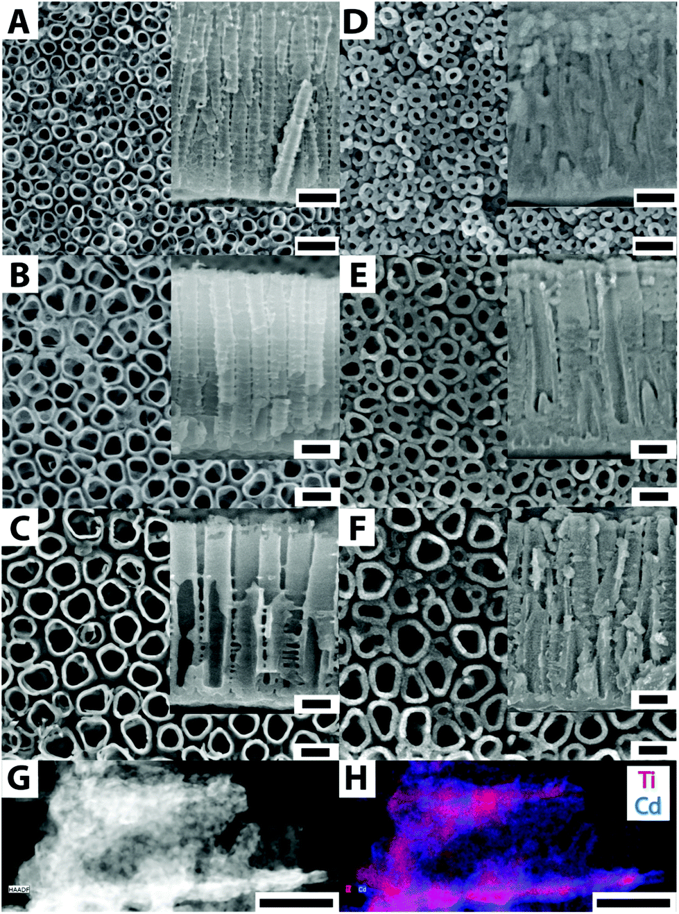 | ||
| Fig. 1 SEM top-view images of the self-organized TiO2 nanotube layers with different average nanotube diameters annealed at 400 °C: (A) 35 nm, (B) 56 nm, and (C) 95 nm. SEM images D–F represent the top-view images of the corresponding TiO2 nanotube layers coated with CdS via ALD. Cross-sectional SEM images of the corresponding TiO2 nanotube layers and CdS-coated counterparts are shown as insets. (G) STEM image of a fragment of CdS-coated TiO2 nanotube, (H) EDX map of the corresponding STEM image showing Cd and Ti distribution. All scale bars show the distance of 100 nm. | ||
Fig. 1G and H show an STEM image and an EDX map, respectively, of the CdS-coated nanotube shown in Fig. 1F. Evidently, the Cd species (forming CdS) are present throughout the TiO2 nanotube, in line with the expectation of a uniform ALD coating.27,28
It was supposed that the significant increase in the number of nanotubes per cm2 could have the potential to enhance the photocurrent response of the heterostructured solar cells due to an increase in the interfacial surface area between the chromophore (produced as a conformal coating by ALD) and the TiO2 nanotube layers. The estimated overall surface areas obtained via simple calculations per 1 cm2 of the TiO2 nanotube layer for the used TiO2 nanotube layers are as follows: 52, 29, and 23 cm2/cm2 of the macroscopic geometrical area for 35, 56, and 95 nm inner diameters of the TiO2 nanotubes, respectively.
To obtain information about the photoelectrochemical properties of the nanotube layers and the CdS-coated TiO2 nanotube layer heterostructures, photocurrent measurements were carried out in an aqueous electrolyte containing 0.1 M Na2SO4via employing a photoelectric spectrophotometer (Instytut Fotonowy) in the wavelength range of 300–650 nm at 0.4 V vs. Ag/AgCl reference electrode.21 Apparently, the coupling of CdS coatings with TiO2 nanotube layers causes a strong sensitizing effect, as shown in Fig. 2. First, the photocurrent density under UV light is enhanced several times as compared to that of the blank TiO2 nanotube layers. We believe that this phenomenon is related to the annihilation of the surface states during ALD of CdS, which significantly improves the charge collection efficiency, as demonstrated in previous works.20,21,30,31 More importantly, a robust photocurrent density can be observed in the visible spectral range, peaking at a wavelength of 470 nm. The obtained incident photon-to-electron conversion efficiencies (IPCE), as shown in Fig. 2B, are significantly higher than the previously reported values for chalcogenide-sensitized TiO2 nanotube layers obtained by chemical bath deposition,8,19 spincoating,20,21 and electrodeposition;22 this is due the fact that the ALD coating of CdS leads to the largest possible interfacial contact area with the TiO2 nanotube layers obtained from these techniques.
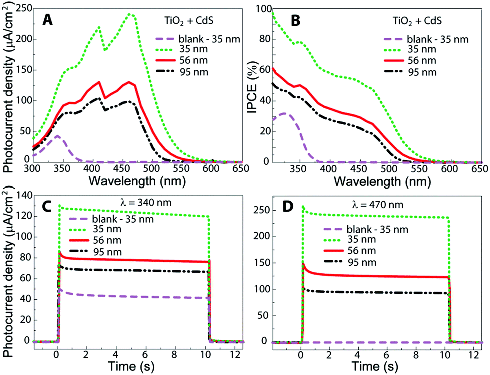 | ||
| Fig. 2 (A) Photocurrent density and (B) incident photon-to-electron conversion efficiency; (C) and (D) photocurrent transients at 340 nm and 470 nm, respectively, obtained for anatase TiO2 nanotube layers annealed at 400 °C with different diameters sensitized with crystalline CdS films deposited via ALD. | ||
In addition, we found that the obtained photocurrent density increased approximately by a factor of 2 with the downscaling of the TiO2 nanotube diameter from 95 to 35 nm in the spectral range from 300 to 500 nm. This result perfectly coincides with the increased active surface area of the TiO2 nanotube layers in the same range of nanotube diameters. Thus, our findings corroborate the assumption that an increase of the interfacial surface area between the chromophore and the TiO2 nanotube layers should generate higher photocurrent density due to the larger amount of CdS absorber deposited via ALD. Conclusively, the combination of 1D nanostructured TiO2 nanotube layers with a thin light absorber deposited via ALD opens a door for a new approach for the fabrication of efficient novel hybrid solar cells. For the energy diagram of the CdS/TiO2 heterostructure, we refer to previously reported literature.25,32
Further, we investigated the influence of thermal treatment of the uncoated TiO2 nanotube layers on the photoresponse of the subsequently prepared heterostructures based on CdS-coated TiO2 nanotube layers. For this experiment, we selected nanotube layers with an inner diameter of 35 nm since they have demonstrated the highest IPCE in the entire spectral range (300–650 nm). It can be seen from Fig. 3A and B that photocurrent densities and IPCE of the CdS-coated TiO2 heterostructures increased with the increasing temperature prior to annealing of the TiO2 nanotube layers in the temperatures range from 300 to 600 °C.
 | ||
| Fig. 3 (A) Photocurrent density and (B) incident photon-to-electron conversion efficiency (IPCE) obtained for the anatase TiO2 nanotube layers with a 35 nm inner diameter annealed at 300, 400, 500, and 600 °C and sensitized with crystalline CdS films via ALD. (C) to (F) represent the top view SEM images of the CdS-coated TiO2 nanotube layers annealed at (C) 300 °C, (D) 400 °C, (E) 500 °C, and (F) 600 °C. | ||
The enhancement in IPCE is not linear with the increasing temperature and can be divided into 3 steps. The most intensive improvement in IPCE was observed when TiO2 nanotube layers were pre-annealed from 300 to 400 °C. Next, it seems that annealing of TiO2 nanotube layers at 400 and 500 °C has a similar effect while annealing at 600 °C, which leads to the anatase to rutile transition,29 adds further contribution to IPCE.
To obtain a deeper understanding of this phenomenon, we obtained the FE-SEM top-view images of the CdS-coated TiO2 nanotube layers (see Fig. 3C–F) in combination with the X-ray diffraction patterns (see Fig. 4). At first, it can be seen that the level of the TiO2 nanotube layer coverage by CdS is noticeably different. While the TiO2 nanotube layers pre-annealed at 300 °C are decorated with the CdS nanoparticles, as demonstrated in Fig. 3C, a compact and uniform CdS crystalline coating is formed on the TiO2 nanotube layers pre-annealed at 400, 500, and 600 °C (see Fig. 3D–F). These results indicate that CdS deposition on TiO2 nanotubes via ALD strongly depends on the TiO2 crystallinity. In the case of TiO2 nanotube layers pre-annealed at 300 °C, the incubation time for CdS nucleation seems to be longer than that for all other samples pre-annealed at higher temperatures. As a consequence of this, these TiO2 nanotube layers are only decorated by CdS nanoparticles, leading to lower total mass of CdS and thus lower IPCE. Since it is evident from XRD that the background in the range of 2 theta from 10 to 22° has different shape for this particular TiO2 nanotube layer pre-annealed at 300 °C, indicating the presence of an amorphous phase, it can be speculated that the CdS nanoparticle growth can be attributed to the incomplete transformation of the originally amorphous TiO2 nanotubes to the anatase phase. On the other hand, TiO2 nanotube layers pre-annealed at higher temperatures template the crystal growth of CdS, which corresponds to the well-evolved crystals. Overall, these findings are well supported by the literature stating that different crystallinity of substrates used for ALD leads to different ALD deposition progress.33,34
 | ||
| Fig. 4 Bragg diffractions of the TiO2 nanotube layers with a 35 nm inner diameter annealed at 300, 400, 500, and 600 °C and sensitized with crystalline CdS films deposited by ALD (left panel). The HRTEM image of the TiO2 nanotube layer pre-annealed at 400 °C and coated with CdS (right panel). | ||
The templating effect is also obvious from the XRD patterns and the HRTEM image. CdS crystallizes in the hexagonal phase within the space group P63mc35 and lattice parameters a = 4.16 Å and c = 6.68 Å. Both the anatase and the rutile modifications possess one cubic face with the lattice parameters a = 3.784 Å (space group I41/amd)36 and a = 4.594 Å (space group P42/mnm),36 which results in lattice mismatches with CdS 10% and 10.4%, respectively. Since the lattice mismatch between CdS and TiO2 phases is small, the nucleation and subsequent crystal growth can proceed fast. From the XRD patterns, it can be seen that CdS crystallizes with the preferential orientation along the crystallographic plane (002), which is more pronounced with increasing pre-annealing temperature of the TiO2 nanotube layers. This observation also supports the idea that fully crystalline TiO2 nanotube layers, pre-annealed at temperatures at/above 400 °C, are suitable matrices for the ALD deposition of uniform CdS coatings.
Conclusions
We presented photoelectrochemical results for anodic TiO2 nanotube layers grown with different diameter sizes (35, 56, and 95 nm) with a thickness of approx. 600 nm sensitized with 6 nm thick CdS coatings deposited via ALD. We found that the obtained photocurrents increased approximately by a factor of 2 with the downscaling of the TiO2 nanotube diameter from 95 to 35 nm in the spectral range from 300 to 500 nm. The result perfectly coincides with the increased active surface area of the TiO2 nanotube layers in the same range of nanotube diameters. We also demonstrated the effect of annealing temperature of TiO2 nanotube layers on the photocurrent generation of the CdS-coated TiO2 nanotube layer photochemical cell. This study unequivocally showed that nanotube layers pre-annealed at temperatures higher than 400 °C generated higher photocurrent density in the spectral range from 350 to 550 nm than the nanotube layers pre-annealed at 300 °C due to the presence of an amorphous phase. Finally, we showed the added value of ALD for uniform coating of the nanotube layers by a functional secondary material.Acknowledgements
European Research Council (project no. 638857) and Ministry of Youth, Education and Sports of the Czech Republic (projects no. LM2015082 and CZ.02.1.01/0.0/0.0/16_013/0001829) are acknowledged for financial support of this work. We thank Dr. Veronika Podzemna, assoc. prof. Ludvik Benes and Dr. Klara Cepe (RCPTM Olomouc) for SEM, XRD and HRTEM analyses, respectively.Notes and references
- M. A. Green, K. Emery, Y. Hishikawa, W. Warta and E. D. Dunlop, Prog. Photovoltaics, 2016, 24, 905–913 Search PubMed.
- D. E. Carlson and C. R. Wronski, Appl. Phys. Lett., 1976, 28, 671 CrossRef CAS.
- J. Britt and C. Ferekides, Appl. Phys. Lett., 1993, 62, 2851 CrossRef CAS.
- P. Jackson, D. Hariskos, E. Lotter, S. Paetel, R. Wuerz, R. Menner, W. Wischmann and M. Powalla, Prog. Photovoltaics, 2011, 19, 894–897 CAS.
- T. K. Todorov, J. Tang, S. Bag, O. Gunawan, T. Gokmen, Y. Zhu and D. B. Mitzi, Adv. Energy Mater., 2013, 3, 34–38 CrossRef CAS.
- B. O'Regan and M. Grätzel, Nature, 1991, 353, 737–740 CrossRef.
- A. Kojima, K. Teshima, Y. Shirai and T. Miyasaka, J. Am. Chem. Soc., 2009, 131, 6050–6051 CrossRef CAS PubMed.
- W.-T. Sun, Y. Yu, H.-Y. Pan, X.-F. Gao, Q. Chen and L.-M. Peng, J. Am. Chem. Soc., 2008, 130, 1124–1125 CrossRef CAS PubMed.
- D. Zhao and Ch.-F. Yang, Renewable Sustainable Energy Rev., 2016, 24, 1048–1059 CrossRef.
- H. Wang, G. Wang, Y. Ling, M. Lepert, C. Wang, J. Z. Zhang and Y. Li, Nanoscale, 2012, 4, 1463–1466 RSC.
- M. Liu, M. M. Johnston and H. J. Snaith, Nature, 2013, 501, 395–398 CrossRef CAS PubMed.
- J. M. Macak, H. Tsuchiya, A. Ghicov, K. Yasuda, R. Hahn, S. Bauer and P. Schmuki, Curr. Opin. Solid State Mater. Sci., 2007, 11, 3–18 CrossRef CAS.
- S. So, I. Hwang and P. Schmuki, Energy Environ. Sci., 2015, 8, 849–854 CAS.
- W. S. Kim, Y. G. Jang, D. H. Kim, H. C. Kim and S. H. Hong, CrystEngComm, 2012, 14, 4963–4966 RSC.
- Y. J. Hwang, C. Hahn, B. Liu and P. Yang, ACS Nano, 2012, 6, 5060–5069 CrossRef CAS PubMed.
- X. Li, J. Yu, J. Low, Y. Fang, J. Xiao and X. Chen, J. Mater. Chem. A, 2015, 3, 2485–2534 CAS.
- H. Mirabolghasemi, N. Liu, K. Lee and P. Schmuki, Chem. Commun., 2013, 49, 2067–2069 RSC.
- Z. Miao, D. Xu, J. Ouyang, G. Guo, X. Zhao and Y. Tang, Nano Lett., 2002, 2, 717–720 CrossRef CAS.
- X. F. Gao, H. B. Li, W. T. Sun, Q. Chen, F. Q. Tang and L. M. Peng, J. Phys. Chem. C, 2009, 113, 7531–7535 CAS.
- J. M. Macak, T. Kohoutek, L. Wang and R. Beranek, Nanoscale, 2013, 5, 9541–9545 RSC.
- M. Krbal, H. Sopha, V. Podzemna, S. Das, J. Prikryl and J. M. Macak, J. Phys. Chem. C, 2017, 121, 6065–6071 CAS.
- J. A. Fernandes, P. Migowski, Z. Fabrim, A. F. Feil, G. Rosa, S. Khan, G. J. Machado, P. F. P. Fichtner, S. R. Teixeira, M. J. L. Santos and J. Dupont, Phys. Chem. Chem. Phys., 2014, 16, 9148–9153 RSC.
- S. Das, H. Sopha, M. Krbal, R. Zazpe, V. Podzemna, J. Prikryl and J. M. Macak, ChemElectroChem, 2017, 4, 495–499 CrossRef CAS PubMed.
- S. S. Kalanur, S. H. Lee, Y. J. Hwang and O.-S. Joo, J. Photochem. Photobiol., A, 2013, 259, 1–9 CrossRef CAS.
- F. Tian, D. Hou, F. Hu, K. Xie, X. Qiao and D. Li, Appl. Surf. Sci., 2017, 391, 295–302 CrossRef CAS.
- H. Cai, Q. Yang, Z. Hu, Z. Duan, Q. You, J. Sun, N. Xu and J. Wu, Appl. Phys. Lett., 2014, 104, 053114 CrossRef.
- R. Zazpe, M. Knaut, H. Sopha, L. Hromadko, M. Albert, J. Prikryl, V. Gärtnerova, J. W. Bartha and J. M. Macak, Langmuir, 2016, 32, 10551–10558 CrossRef CAS PubMed.
- R. Zazpe, J. Prikryl, V. Gärtnerova, K. Nechvilova, L. Benes, L. Strizik, A. Jäger, M. Bosund, H. Sopha and J. M. Macak, Langmuir, 2017, 33, 3208–3216 CrossRef CAS PubMed.
- S. Das, R. Zazpe, J. Prikryl, P. Knotek, M. Krbal, H. Sopha, V. Podzemna and J. M. Macak, Electrochim. Acta, 2016, 213, 452–459 CrossRef CAS.
- J. W. Zheng, A. Bhattcahrayya, P. Wu, Z. Chen, J. Highfield, Z. Dong and R. Xu, J. Phys. Chem. C, 2010, 114, 7063–7069 CAS.
- T. Umebayashi, T. Yamaki, H. Itoh and K. Asai, Appl. Phys. Lett., 2002, 81, 454–456 CrossRef CAS.
- Y.-L. Lee and Y.-S. Lo, Adv. Funct. Mater., 2009, 19, 604–609 CrossRef.
- R. S. Pessoa, F. P. Pereira, G. E. Testoni, W. Chiappim, H. S. Maciel and L. V. Santos, J. Integr. Circuits Syst., 2015, 10, 38–42 Search PubMed.
- H. B. R. Lee and S. Bent, Chem. Mater., 2012, 24, 279–286 CrossRef CAS.
- A. A. Andreev, M. F. Bulanyi, S. A. Golikov and L. A. Mozharovsikii, Russ. J. Inorg. Chem., 1995, 40, 1039–1042 Search PubMed.
- D. W. Kim, N. Enomoto, Z. Nakagawa and K. Kawamura, J. Am. Ceram. Soc., 1996, 79, 1095–1099 CrossRef CAS.
| This journal is © The Royal Society of Chemistry 2017 |