
 Open Access Article
 This Open Access Article is licensed under a
 Creative Commons Attribution 3.0 Unported Licence
Low temperature growth of fully covered single-layer graphene using a CoCu catalyst†
Hisashi
Sugime
 *ab,
Lorenzo
D'Arsié
b,
Santiago
Esconjauregui
b,
Guofang
Zhong
b,
Xingyi
Wu
b,
Eugen
Hildebrandt
b,
Hikmet
Sezen
c,
Matteo
Amati
c,
Luca
Gregoratti
c,
Robert S.
Weatherup
b and
John
Robertson
b
*ab,
Lorenzo
D'Arsié
b,
Santiago
Esconjauregui
b,
Guofang
Zhong
b,
Xingyi
Wu
b,
Eugen
Hildebrandt
b,
Hikmet
Sezen
c,
Matteo
Amati
c,
Luca
Gregoratti
c,
Robert S.
Weatherup
b and
John
Robertson
b
aWaseda Institute for Advanced Study, Waseda University, Tokyo 169-8050, Japan. E-mail: sugime@aoni.waseda.jp; Tel: +81-3-5286-2769
bDepartment of Engineering, University of Cambridge, Cambridge CB3 0FA, UK
cElettra-Sincrotrone Trieste S.C.p.A., AREA Science Park, S.S. 14 km 163.5, 34149, Trieste, Italy
First published on 28th August 2017
Abstract
A bimetallic CoCu alloy thin-film catalyst is developed that enables the growth of uniform, high-quality graphene at 750 °C in 3 min by chemical vapour deposition. The growth outcome is found to vary significantly as the Cu concentration is varied, with ∼1 at% Cu added to Co yielding complete coverage single-layer graphene growth for the conditions used. The suppression of multilayer formation is attributable to Cu decoration of high reactivity sites on the Co surface which otherwise serve as preferential nucleation sites for multilayer graphene. X-ray photoemission spectroscopy shows that Co and Cu form an alloy at high temperatures, which has a drastically lower carbon solubility, as determined by using the calculated Co–Cu–C ternary phase diagram. Raman spectroscopy confirms the high quality (ID/IG < 0.05) and spatial uniformity of the single-layer graphene. The rational design of a bimetallic catalyst highlights the potential of catalyst alloying for producing two-dimensional materials with tailored properties.
Introduction
Graphene's 2D structure, excellent electronic properties, and chemical stability1–4 make it a promising material for device applications including transparent electrodes, sensors, and passivating layers.5–7 Chemical vapour deposition (CVD) has emerged as the most scalable and versatile technique to grow graphene for such applications, where a high-quality material is typically required.8,9 Uniform single-layer graphene (SLG) has been well demonstrated on low-cost polycrystalline Cu foils over a broad window of processing conditions,10–13 leading to the widespread adoption of Cu-based catalysts, with full coverage SLG consisting of millimetre-scale domains achievable through appropriate catalyst treatments.14 To obtain large domain sizes and low defect densities, growth is typically performed at relatively high growth temperatures (>1000 °C) on thick catalyst foils (∼25 μm).15 These conditions are not readily compatible with many established device materials or thin-film patterning/processing methods, limiting the potential for direct integration. Current approaches to device fabrication from CVD graphene therefore rely for the most part on transfer to a target substrate, which is far from straightforward, with many opportunities for deleterious contamination and mechanical damage to be introduced.16 Furthermore, given that significant Cu sublimation leads to roughening of the catalyst surface at the growth temperature,17 there is inevitable wrinkling of the material when it is transferred to the target substrate. For direct integration, methods are therefore needed to grow high-quality SLG on selected thin-film materials at low temperatures, allowing facile incorporation into device structures,18,19 as well as increased scalability and reduced production costs. This requires the rational design of the catalyst support and growth process to achieve a desired outcome, which is only possible through a detailed understanding of the underlying growth mechanisms and how they can be controlled.At lower temperatures, Ni, Co, and Fe show higher catalytic activities than Cu, both for hydrocarbon dissociation and carbon incorporation into graphitic structures. Indeed, they have been widely employed as catalysts for the low temperature growth of carbon nanotubes.20–27 However, attempts to grow polycrystalline thin-films of these metals have generally resulted in the formation of inhomogeneous multi-layer graphene.28–33 This has often been attributed to the high carbon solubility of these metals, based on the assumption that carbon dissolved in the catalyst precipitates as multilayer graphene on cooling.11,34 However, extensive in situ studies confirm that growth, including multilayer formation, occurs predominantly isothermally at typical growth temperatures.35–44 This multilayer formation is related to high catalytic activity of these catalysts which can result in direct multilayer nucleation, or the thin-film catalysts becoming rapidly saturated with carbon throughout their thickness with additional carbon dissociation feeding multilayer formation.45,46 This can be avoided by using thick catalyst foils, where the supply of carbon from the gas-phase is mediated by ongoing carbon diffusion into the catalyst bulk, resulting in a broad processing window over which uniform SLG can be stabilised.45,46 Alternatively single-crystalline substrates may be used, where careful control of the exposure conditions can yield epitaxial, SLG on specific surface orientations.38,40,43,47,48 However neither of these approaches can be readily integrated with standard lithographic processing steps used in fabricating device structures.
Catalyst alloying provides a means of tuning surface reactivity that can be directly applied to thin-film catalyst materials. For example, by decorating high-reactivity sites on polycrystalline Ni with Au we have previously demonstrated the suppression of multilayer growth, with uniform SLG formed at temperatures as low as 450 °C.37,41,45,49 On the other hand, widening the selection of ferromagnetic materials on which SLG can be formed is of significant importance for applications. For example, SLG-covered Co electrodes show enhanced perpendicular magnetic anisotropy,50 remain stable against oxidation in air,7,51 and are promising as spin filtering electrodes.52 However, the low temperature growth of SLG with thin Co catalysts has not been reported. In this paper, we consider the addition of less catalytically active Cu to the surface of Co thin-films, to tune the graphene growth behaviour. Using an original combinatorial method,53,54 we investigate the effect of the alloy ratio on the growth of graphene, and find that there is an optimum thickness for Cu to maximize the coverage of SLG. With the optimum condition, we demonstrate the formation of full coverage, high quality SLG on sputtered CoCu catalyst films with a simple thermal CVD process at relatively low temperatures. The underlying mechanisms that lead to this improvement are systematically investigated using ex situ growth calibrations, in situ scanning photoemission microscopy (SPEM), and calculated ternary phase diagrams. The Cu is found to decorate high reactivity sites on the Co surface, suppressing multilayer graphene nucleation and resulting in exclusively SLG formation. We thereby demonstrate that the approach of catalyst alloying can be extended to tune graphene growth on different transition metal catalysts, offering new opportunities for directly integrating graphene into device structures.
Results
We first investigate the effect of the catalyst composition on the graphene growth using combinatorial CoCu samples. Fig. 1a shows a schematic of the combinatorial method.53,54 We make a thickness gradient of Cu (∼0.3–20 nm) on uniform Co (500 nm) in one direction (∼10 mm in length) by using a slit mask. The area with the thickest Cu (∼20 nm) appears slightly orange in colour before graphene growth (left area in Fig. 1b). Fig. 1c shows SEM images of graphene grown on the CoCu catalyst at 750 °C for 3 min, and OM images following transfer of the graphene to SiO2 (300 nm)/Si. The Cu thickness range considered in Fig. 1c corresponds to the area shown with the dashed rectangle in the Fig. 1b. Depending on the Cu thickness, the graphene grows with different nucleation densities, numbers of layers, and grain sizes. Multilayer graphene grows when the Cu adlayer is less than ∼2.4 nm thick (right part of Fig. 1c). We note that the contrast associated with multilayer graphene is most apparent in the OM images following transfer of the graphene onto SiO2(300 nm)/Si.55,56 Increasing the Cu thickness to ∼3.8 nm results in a SLG coverage of ∼90%, whilst with ∼6.0 nm of Cu full SLG coverage is achieved as highlighted with the red rectangle in Fig. 1c. Further increasing the Cu thickness results in the formation of bilayer and multilayer graphene regions as readily apparent with ∼10 nm of Cu (leftmost images in Fig. 1c). | ||
| Fig. 1 (a) A schematic of the combinatorial method where sputtering Cu through a slit mask yields a thickness gradient (∼0.3–20 nm) on top of uniform Co (500 nm). (b) Optical image of the combinatorial sample before growth. (c) SEM images of the as-grown graphene on different regions of the catalyst with different Cu thicknesses (∼1.5–10 nm) and corresponding OM images following transfer of the graphene onto SiO2 (300 nm)/Si substrates. The scale bar in (c) is common for the SEM and the OM images. The Cu thickness range shown in (c) corresponds to the area of the sample shown with a dashed rectangle in (b). | ||
Our focus herein is obtaining uniform SLG coverage, and therefore we further investigate samples with Cu (6.0 nm) uniformly deposited over Co (500 nm) and compare these to bare Co (500 nm). Fig. 2a and b show the SEM and OM images of graphene films grown on Co, and CoCu under the same conditions as in Fig. 1 (750 °C, 3 min). The SEM images are acquired from the as-grown graphene on the catalyst while the OM images are taken after transferring the graphene to SiO2(300 nm)/Si substrates. As observed with the combinatorial samples in Fig. 1, the sample with elemental Co yields complete coverage with inhomogeneous multilayer graphene, while the CoCu sample is completely covered with uniform SLG. We note that if the Ti adhesion layer is not present under the Co film, it is found to dewet at high temperature and form holes of ∼300 nm diameter (see Fig. S1†).
 | ||
| Fig. 2 SEM and OM images of fully covered graphene grown on (a) Co (500 nm) and (b) CoCu [Cu: 6 nm on Co: 500 nm] catalyst. (c) Representative Raman spectra of the samples shown in (a) and (b). Raman maps of (d) I2D/IG ratio, (e) ID/IG ratio, and (f) FWHM (2D) of the CoCu sample shown in (a) measured over a 40 × 40 μm2 area at a pitch of 2 μm. The scale bars in (a) and (b) are common for SEM and OM images, respectively. | ||
Fig. 2c shows the Raman spectra of the samples in Fig. 2a and b. With the elemental Co sample, we observe the D-peak at 1348 cm−1, the G-peak at 1582 cm−1 with full width at half maximum (FWHM) of 36 cm−1, and the 2D-peak at 2697 cm−1 (FWHM: 96 cm−1). The ID/IG ratio is 0.18 and the I2D/IG ratio is 0.61, which along with the large FWHM of the 2D-peak are consistent with those reported for reasonably defective multilayer graphene. With the CoCu sample, on the other hand, we observe a very small D-peak at 1359 cm−1, the G-peak at 1593 cm−1 (FWHM: 16 cm−1), and the 2D-peak at 2683 cm−1 (FWHM: 35 cm−1). The small ID/IG ratio of under 0.05, I2D/IG ratio of 2.1, and narrow 2D-peak which is well-fitted by a single-lorentzian confirm the presence of high quality SLG.57 We note that there is an increase in the ID/IG ratio to 0.38 as the growth temperature is lowered to 700 °C (50 °C lower than the standard condition) indicating deterioration in the graphene crystallinity (see Fig. S2†). For the CoCu sample grown under standard conditions, we perform Raman mapping over a 40 × 40 μm2 area with a pitch of 2 μm. Fig. 2d, e, and f show maps of the I2D/IG ratio, ID/IG ratio, and 2D FWHM, respectively. In the mapped area, it is confirmed that 95% has a I2D/IG ratio >1.8, 93% has a ID/IG ratio <0.10, and 94% has a FWHM <39 cm−1 which confirms the good spatial uniformity of the SLG. In addition to Raman spectroscopy which gives a relatively direct measure of defect density based on the ID/IG ratio,58 we have also measured the carrier mobility of the graphene which provides a more indirect indicator of graphene quality. Hall effect measurements on a device made from the graphene on SiO2(300 nm)/Si reveal that the hole mobility is ∼1100 cm2 V−1 s−1 for a carrier concentration of ∼3.9 × 1012 cm−2 under ambient conditions. The carrier concentration herein shows a slightly higher value than that of graphene grown on elemental Cu catalysts in our previous study (∼1.5 × 1012 cm−2) with the same measurement setup.59 However we note that this falls within the variation expected as a result of the transfer process and processing in air, where polymer and etchant residues and air-borne contaminants can alter the doping.
We now consider the differences in the graphene nucleation and the domain growth on the CoCu and Co by varying the growth time whilst otherwise keeping the same growth conditions as used in Fig. 1. After 20 s of exposure to the carbon precursor (CH4), no graphene grows on the Co (Fig. 3a). After 100 s, multilayer graphene domains with diameters of several tens of μm appear and already starts to merge, giving an areal coverage of ∼80% (Fig. 3b). Complete multilayer graphene is observed for samples exposed to the carbon precursor for 180 s (Fig. 3c). In contrast, after 20 s of exposure to the carbon precursor (CH4), the CoCu surface shows the presence of dark spots several tens of nanometres in size (indicated by arrows in the inset of Fig. 3d) with a number density of ∼60 μm−2. After 100 s, SLG domains of up to 25 μm in diameter are present with an areal coverage of ∼10%. This corresponds to an ∼8 times smaller areal coverage than that observed for elemental Co with the same growth time, and in fact corresponds to an even smaller extent of graphene formation as only single-layer domains are formed. Domains with diameters as small as a few micrometres are observed, as shown by arrows and the ×10 enlargement of a region of the image in Fig. 3e. Besides these micrometre-scale graphene domains, we also observe dark spots which are at least a hundred times smaller and resemble those obtained after 20 s (arrow indications in the inset of Fig. 3e). After 180 s, the micrometre-scale domains merge with each other, resulting in complete coverage of the catalyst surface (Fig. 3f).
 | ||
| Fig. 3 SEM images of the surface of (a–c) Co (500 nm) and (d–f) CoCu [Cu: 6 nm on Co: 500 nm] samples with different growth times. The scale bars in (a) are common for all the low magnification images and the higher magnification insets, respectively. | ||
To further investigate the chemical influence of Cu on the Co catalyst surface, we perform in situ XPS measurements during the annealing of CoCu [Cu: 6 nm on Co: 500 nm] and Co (500 nm) samples. Fig. 4a and b show Cu 2p3/2 and Co 2p3/2 XP spectra of the CoCu sample, and Fig. 4c shows the Co 2p3/2 XP spectra of the elemental Co sample at salient stages during annealing in 10−6 mbar of H2. The Cu 2p3/2 spectrum of the CoCu sample at room temperature (RT) shows a single peak at 932.0 eV, characteristic of Cu2O.60 During annealing under H2, the Cu2O peak decreases in intensity while a peak at 932.6 eV rises indicating the reduction of Cu2O towards metallic Cu, with no Cu2O remaining at 550 °C. A similar reduction behaviour is observed in the Co 2p3/2 spectra of both the CoCu and the elemental Co samples. At temperatures below 200 °C the spectra correspond to predominantly oxidised Co (blue components), while at higher temperatures Co is gradually reduced, showing a complete reduction at 550 °C (green metallic peaks).
 | ||
| Fig. 4 In situ XPS spectra [photon energy: 1102 eV] of (a) Cu 2p3/2 and (b) Co 2p3/2 of the CoCu [Cu: 6 nm on Co: 500 nm] sample, and (c) Co 2p3/2 of the elemental Co (500 nm) sample at different temperatures during annealing in H2 (∼1 × 10⁻⁶ mbar). A Shirley background is used and the peaks are fitted with Doniach–Sunjic functions convoluted with Gaussian profiles. | ||
No peaks are detectable in the Co 2p3/2 spectrum of the CoCu sample at RT, as the photoemission signal is dominated by the Cu film at the surface, which has a thickness of 6 nm. The signal, however, progressively rises above the noise as the temperature is increased (from roughly 200 °C). A chemical map of Cu obtained at 550 °C using SPEM (with 100 nm lateral resolution) shows a uniformly low Cu signal without any significant lateral inhomogeneity in the Cu distribution (Fig. S3†), indicating that the Cu diffuses into the Co substrate rather than simply redistributing at the surface. This is further confirmed by the difference in asymmetry (alpha) of the main metallic peak of Co in the 550 °C spectrum of both CoCu (alpha ∼0.20) and elemental Co (alpha ∼0.14) samples. The increased asymmetry of the Co peak for the CoCu sample is linked to a higher density of states (DOS) at the Fermi edge61 compared to the elemental Co sample,62 consistent with alloying of Co with Cu. The Co–Cu binary phase diagram shows a miscibility gap for the temperature range considered here, with the Co-rich phase having a Cu solubility of ∼1 at% at 750 °C whilst above this level Co- and Cu-rich phases coexist.63,64 Thus for the thickness ratio investigated here [Cu: 6 nm on Co: 500 nm, i.e. ∼1 at%], we expect a Co-rich alloy to be formed that is almost saturated with Cu.
To further understand the role that this alloying plays in growth, we calculate a Co–Cu–C ternary phase diagram using the Thermo-calc package.65Fig. 5 shows a part of the calculated phase diagram where small amounts of Cu and/or C (≤0.4 at%) are present as a solid solution in Co at 750 °C. As the amount of Cu is increased, a FCC(ordered) phase emerges in FCC(L12) which has almost no carbon solubility. The carbon solubility in Co therefore drastically decreases from ∼0.23 at% in pure Co to nearly zero when alloying with ∼0.23 at% of Cu (arrow indication in Fig. 5).
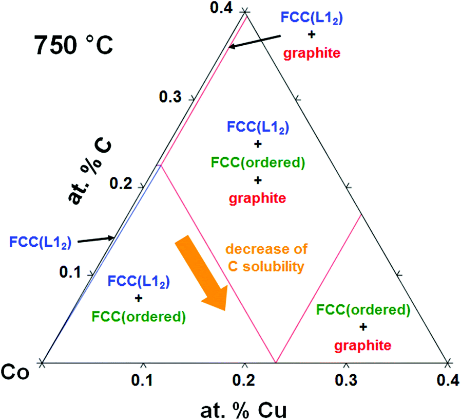 | ||
| Fig. 5 Part of the Co–Cu–C ternary phase diagram calculated using Thermo-Calc and SSOL5 database. | ||
Based on our results, and in the context of previous literature we now explain the origins of the different graphene growth behaviours on elemental Co and CoCu catalysts, as summarized in Fig. 6. Although Co has a relatively high carbon solubility, our previous in situ studies of graphene growth on catalysts with comparable or even higher carbon solubilities (Ni, Pt),37,39,41,43,44 and similar reports in the literature35,36,38,42,66,67 show that isothermal growth typically dominates at the temperature considered here, with precipitation on cooling remaining a minor contribution due to the rapid decrease in carbon diffusivity with temperature.46 We therefore note that the graphene growth observed herein is expected to occur predominantly isothermally i.e. at temperature during the hydrocarbon exposure, and have further confirmed this with in situ XPS measurements performed on Co thin films at similar temperatures.68 For elemental Co, during the early stages of hydrocarbon exposure (∼20 s) there is a significant incubation period where no graphene nucleation occurs (Fig. 3a and 6a) as the supply of carbon from hydrocarbon dissociation is matched by diffusion into the Co bulk due to its relatively high carbon solubility (0.23 at% at 750 °C, see Fig. 5). With continuing exposure the carbon concentration at the Co surface increases until it exceeds the solubility limit leading to the preferential nucleation of multilayer graphene at high reactivity surface sites such as step edges (Fig. 3b and 6b).37,45 After 180 s, a continuous multilayer graphene film has been formed (Fig. 2a, 3c, and 6c), which is consistent with the many other reports of multilayer graphene formation on polycrystalline thin films of elemental Co.31–33,46,48
 | ||
| Fig. 6 Schematics of the graphene growth mechanism on Co and CoCu catalyst. | ||
For the CoCu catalyst we observe that dark spots of several tens of nanometres in size form on the surface within just 20 s of hydrocarbon exposure (Fig. 3d and 6d), whilst no similar spots are observed on the elemental Co for the same exposure time (Fig. 3a). This difference is attributed to the lower carbon solubility of the CoCu alloy, as shown by the Co–Cu–C ternary phase diagram in Fig. 5, which means that there is limited carbon diffusion into the catalyst bulk but instead the carbon supplied to the surface in the initial stages of hydrocarbon exposure remains at the catalyst surface forming these dark spots. As growth proceeds, exclusively SLG domains nucleate and grow on the catalyst surface (Fig. 3e and 6e). In situ XPS reveals that Cu remains at the catalyst surface following annealing, and is thus present at the point of hydrocarbon introduction. We therefore attribute this suppression of multilayer graphene formation to the Cu decorating and passivating high reactivity sites on the Co surface (e.g. step edges) which are preferential nucleation sites for multilayer graphene,69,70 as has also been previously demonstrated for Ni surfaces decorated with Au. These same high reactivity sites are implicated in hydrocarbon dissociation, and thus their decoration with Cu is also expected to reduce the hydrocarbon dissociation rate (as highlighted by a smaller arrow in Fig. 6d).23 Indeed, the much lower graphene coverage seen for CoCu after 100 s, in spite of its lower C solubility and thus smaller expected incubation time, is fully consistent with this picture. Extending the exposure time to 180 s leads to the lateral growth of the SLG domains to form a continuous film without any multilayer graphene observed (Fig. 3f and 6f).
Our results show that when the Cu thickness is too low, multilayer graphene formation is not completely suppressed (∼2.4 nm in Fig. 1c), suggesting insufficient decoration of the high-reactivity sites. We also find that too thick a Cu layer leads to the formation of discontinuous multilayer graphene domains (∼10 nm in Fig. 1c), which we attribute to a phase separation (i.e. incomplete alloying) at the catalyst surface, with graphene growth constrained to Co-rich regions whilst the Cu-rich regions remain bare. An intermediate Cu thickness of ∼4–6 nm leads to exclusively SLG formation, whose coverage for a given growth time increases slightly with Cu thickness. This is consistent with the reduction in C solubility, and thus incubation time that is expected as the Cu content of the CuCo alloy is increased. We therefore find that a Cu to Co ratio [Cu: 6 nm on Co: 500 nm] that closely approaches the solubility limit of Cu in Co (∼1 at% at 750 °C) results in the formation of a fully covered uniform SLG film (Fig. 2b, 3f, and 6f). We attribute this to the decoration of high-reactivity surface sites being maximised, whilst phase separation is still avoided.
As well as suppressing multilayer formation, we note that the Co–Cu alloying also leads to a significant improvement in the graphitic quality of the graphene formed, with a lower D-peak apparent in Raman spectra (Fig. 2c). Although we are unable to directly resolve the origins of this improvement with the experimental methods used here, we expect that a lower hydrocarbon dissociation rate, and thus rate of carbon incorporation into existing graphene domains, plays an important role.
The general approach of catalyst alloying to control the layer number and domain sizes when growing 2D materials has been applied with other catalyst systems including Ni–Au,37,41,45 Ni–Mo,71 and Cu–Ni72,73 for graphene, and Fe–Si74 and Cu–Ni75 for hexagonal boron nitride. We show here that a detailed understanding of the underlying growth behaviour allows the rational design of a binary alloy catalyst to achieve improved graphene properties, highlighting that catalyst alloying is a powerful tool in tuning the catalytic growth of 2D materials. This is particularly pertinent for applications of 2D materials where constraints are placed on the processing temperature or catalyst materials that can be used, such as when the 2D material and catalyst are to be directly integrated into devices without any transfer step. This includes applications where the 2D material is used as a passivation layer7,49 or a tunnel barrier.76
Conclusion
We have developed a CoCu bimetallic catalyst thin film for graphene growth that achieves complete SLG coverage in 3 min at 750 °C, and have investigated the underlying growth behaviour. The layer number, incubation time, and growth rate change sensitively depending on the Cu thickness. In situ XPS measurements show that the addition of ∼1 at% Cu (∼6 nm) into Co (500 nm) results in a Co-rich alloy forming at the growth temperature. The Cu decorates high reactivity sites on the Co surface (e.g. step edges), thereby suppressing multilayer graphene nucleation, and resulting in exclusively SLG formation. Raman mapping confirms the high quality (ID/IG < 0.05) and good spatial uniformity of the SLG. The relatively low temperature growth process with a simple thermal CVD using sputtered metal films is suitable for the direct growth and integration of graphene into devices, and highlights that catalyst alloying can be used to produce graphene with tailored properties.Methods
We use Si (100) wafers with a thermal oxide layer (200 nm) as substrates. We deposit Ti (10 nm) as an adhesion layer followed by Co (500 nm) as the catalyst. The deposition is carried out without breaking the vacuum between Ti and Co. After exposing the samples to air, Cu is deposited on top of the Co either uniformly (6 nm) or with a thickness gradient obtained using a combinatorial masked deposition method.53,54 All the depositions are carried out by DC sputtering under Ar (3.5 × 10⁻³ mbar). For the growth of graphene by thermal CVD, the samples are loaded into a cold-wall CVD apparatus. The chamber is pumped below 2.0 × 10⁻² mbar by a screw pump in ∼10 min, and then the samples are heated up to 700–750 °C at a rate of 5 °C s−1 under H2 (240 sccm) with the pressure adjusted to 40 mbar. When the desired temperature is reached, CH4 (60 sccm) is immediately added for 20–180 s to induce graphene growth. The total pressure is kept at 50 mbar during the hydrocarbon exposure (CH4 + H2), and the samples are subsequently cooled down quickly (∼10 °C s−1) under Ar (200 sccm).The as-grown graphene on catalyst metals is characterized by scanning electron microscopy (SEM, Carl Zeiss, SIGMA VP). Optical microscopy (OM) and Raman spectroscopy (Renishaw, InVia spectrometer, 532 nm excitation) measurements are performed following transfer of the graphene onto SiO2(300 nm)/Si substrates using a PMMA support layer and FeCl3 solution (1 M) to dissolve the catalyst layer. We measure the charge carrier mobility of the SLG by the Hall effect using Van der Pauw structures (MMR Technologies, H-50).77 We pattern 20 × 20 μm2 squares of graphene on SiO2(300 nm)/Si substrates by e-beam lithography, where Au(45 nm)/Cr(5 nm) electrodes have already been patterned on the substrate by thermal evaporation and a lift-off process before the transfer of graphene. The measurement is carried out under 1 T magnetic field at room temperature.
In situ X-ray photoemission spectroscopy (XPS) is used to characterize the chemical state of the catalyst metals. The measurements are performed at the ESCAmicroscopy beamline at the Elettra synchrotron (Trieste, Italy). The X-ray beam with a photon energy of 1102 eV is focused on the samples to a diameter of ∼200 nm using Fresnel zone plate optics, and the sample can be raster scanned with respect to the microprobe.78 The sample is measured during annealing under H2 (∼1 × 10⁻⁶ mbar). The spectra are background-corrected (Shirley) and the peaks are fitted with Doniach–Sunjic functions convoluted with Gaussian profiles. A Co–Cu–C ternary phase diagram is calculated using Thermo-Calc and SSOL5 database.65
Author contributions
H. Sugime and R. S. Weatherup designed the experiment, conducted most experiments, and wrote the manuscript. L. D'Arsié, S. Esconjauregui, H. Sezen, M. Amati, and L. Gregoratti carried out the XPS measurements. L. D'Arsié, X. Wu, and G. Zhong carried out the electrical and Raman measurements. X. Wu and E. Hildebrandt carried out the SEM analysis. J. Robertson supervised the project. The manuscript was edited through contributions of all authors.Conflicts of interest
There are no conflicts to declare.Acknowledgements
This work has been funded by the European project Grafol and EPSRC grant EP/P005152/1. H. S. acknowledges a research fellowship from the Japanese Society for the Promotion of Science (JSPS). R. S. W. acknowledges a Research Fellowship from St John's College, Cambridge and a Marie Skłodowska-Curie Individual Fellowship (Global) under grant ARTIST (no. 656870) from the European Union's Horizon 2020 research and innovation programme.Notes and references
- K. S. Novoselov, A. K. Geim, S. V. Morozov, D. Jiang, Y. Zhang, S. V. Dubonos, I. V. Grigorieva and A. A. Firsov, Science, 2004, 306, 666–669 CrossRef CAS PubMed.
- K. S. Novoselov, D. Jiang, F. Schedin, T. J. Booth, V. V. Khotkevich, S. V. Morozov and A. K. Geim, Proc. Natl. Acad. Sci. U. S. A., 2005, 102, 10451–10453 CrossRef CAS PubMed.
- A. K. Geim and K. S. Novoselov, Nat. Mater., 2007, 6, 183–191 CrossRef CAS PubMed.
- A. K. Geim, Science, 2009, 324, 1530–1534 CrossRef CAS PubMed.
- K. S. Novoselov, V. I. Falko, L. Colombo, P. R. Gellert, M. G. Schwab and K. Kim, Nature, 2012, 490, 192–200 CrossRef CAS PubMed.
- A. C. Ferrari, F. Bonaccorso, V. Fal'ko, K. S. Novoselov, S. Roche, P. Boggild, S. Borini, F. H. L. Koppens, V. Palermo, N. Pugno, J. A. Garrido, R. Sordan, A. Bianco, L. Ballerini, M. Prato, E. Lidorikis, J. Kivioja, C. Marinelli, T. Ryhanen, A. Morpurgo, J. N. Coleman, V. Nicolosi, L. Colombo, A. Fert, M. Garcia-Hernandez, A. Bachtold, G. F. Schneider, F. Guinea, C. Dekker, M. Barbone, Z. P. Sun, C. Galiotis, A. N. Grigorenko, G. Konstantatos, A. Kis, M. Katsnelson, L. Vandersypen, A. Loiseau, V. Morandi, D. Neumaier, E. Treossi, V. Pellegrini, M. Polini, A. Tredicucci, G. M. Williams, B. H. Hong, J. H. Ahn, J. M. Kim, H. Zirath, B. J. van Wees, H. van der Zant, L. Occhipinti, A. Di Matteo, I. A. Kinloch, T. Seyller, E. Quesnel, X. L. Feng, K. Teo, N. Rupesinghe, P. Hakonen, S. R. T. Neil, Q. Tannock, T. Lofwander and J. Kinaret, Nanoscale, 2015, 7, 4598–4810 RSC.
- R. S. Weatherup, L. D'Arsié, A. Cabrero-Vilatela, S. Caneva, R. Blume, J. Robertson, R. Schloegl and S. Hofmann, J. Am. Chem. Soc., 2015, 137, 14358–14366 CrossRef CAS PubMed.
- S. Hofmann, P. Braeuninger-Weimer and R. S. Weatherup, J. Phys. Chem. Lett., 2015, 6, 2714–2721 CrossRef CAS PubMed.
- G. Zhong, X. Wu, L. D'Arsie, K. B. K. Teo, N. L. Rupesinghe, A. Jouvray and J. Robertson, Appl. Phys. Lett., 2016, 109, 193103 CrossRef.
- X. S. Li, W. W. Cai, J. H. An, S. Kim, J. Nah, D. X. Yang, R. Piner, A. Velamakanni, I. Jung, E. Tutuc, S. K. Banerjee, L. Colombo and R. S. Ruoff, Science, 2009, 324, 1312–1314 CrossRef CAS PubMed.
- X. Li, W. Cai, L. Colombo and R. S. Ruoff, Nano Lett., 2009, 9, 4268–4272 CrossRef CAS PubMed.
- X. Li, C. W. Magnuson, A. Venugopal, R. M. Tromp, J. B. Hannon, E. M. Vogel, L. Colombo and R. S. Ruoff, J. Am. Chem. Soc., 2011, 133, 2816–2819 CrossRef CAS PubMed.
- H. Zhou, W. J. Yu, L. Liu, R. Cheng, Y. Chen, X. Huang, Y. Liu, Y. Wang, Y. Huang and X. Duan, Nat. Commun., 2013, 4, 2096 Search PubMed.
- X. Wu, G. F. Zhong, L. D'Arsié, H. Sugime, S. Esconjauregui, A. W. Robertson and J. Robertson, Sci. Rep., 2016, 6, 21152 CrossRef CAS PubMed.
- R. Muñoz and C. Gomez-Aleixandre, Chem. Vapor Deposition, 2013, 19, 297–322 CrossRef.
- M. Kratzer, B. C. Bayer, P. R. Kidambi, A. Matković, R. Gajić, A. Cabrero-Vilatela, R. S. Weatherup, S. Hofmann and C. Teichert, Appl. Phys. Lett., 2015, 106, 103101 CrossRef.
- P. R. Kidambi, C. Ducati, B. Dlubak, D. Gardiner, R. S. Weatherup, M.-B. Martin, P. Seneor, H. Coles and S. Hofmann, J. Phys. Chem. C, 2012, 116, 22492–22501 CAS.
- B. Dlubak, M.-B. Martin, R. S. Weatherup, H. Yang, C. Deranlot, R. Blume, R. Schloegl, A. Fert, A. Anane, S. Hofmann, P. Seneor and J. Robertson, ACS Nano, 2012, 6, 10930–10934 CAS.
- M.-B. Martin, B. Dlubak, R. S. Weatherup, H. Yang, C. Deranlot, K. Bouzehouane, F. Petroff, A. Anane, S. Hofmann, J. Robertson, A. Fert and P. Seneor, ACS Nano, 2014, 8, 7890–7895 CrossRef CAS PubMed.
- M. Nihei, A. Kawabata and Y. Awano, Jpn. J. Appl. Phys., 2003, 42, L721–L723 CrossRef CAS.
- M. Cantoro, S. Hofmann, S. Pisana, V. Scardaci, A. Parvez, C. Ducati, A. C. Ferrari, A. M. Blackburn, K. Y. Wang and J. Robertson, Nano Lett., 2006, 6, 1107–1112 CrossRef CAS PubMed.
- D. Yokoyama, T. Iwasaki, K. Ishimaru, S. Sato, T. Hyakushima, M. Nihei, Y. Awano and H. Kawarada, Jpn. J. Appl. Phys., 2008, 47, 1985–1990 CrossRef CAS.
- J. Robertson, J. Mater. Chem., 2012, 22, 19858–19862 RSC.
- H. Sugime, S. Esconjauregui, J. W. Yang, L. D'Arsié, R. A. Oliver, S. Bhardwaj, C. Cepek and J. Robertson, Appl. Phys. Lett., 2013, 103, 073116 CrossRef.
- H. Sugime, S. Esconjauregui, L. D'Arsié, J. W. Yang, T. Makaryan and J. Robertson, ACS Appl. Mater. Interfaces, 2014, 6, 15440–15447 CAS.
- N. Na, D. Y. Kim, Y. G. So, Y. Ikuhara and S. Noda, Carbon, 2015, 81, 773–781 CrossRef CAS.
- H. Sugime, S. Esconjauregui, L. D'Arsié, J. Yang, A. W. Robertson, R. A. Oliver, S. Bhardwaj, C. Cepek and J. Robertson, ACS Appl. Mater. Interfaces, 2015, 7, 16819–16827 CAS.
- Q. Yu, J. Lian, S. Siriponglert, H. Li, Y. P. Chen and S.-S. Pei, Appl. Phys. Lett., 2008, 93, 113103 CrossRef.
- A. Reina, X. Jia, J. Ho, D. Nezich, H. Son, V. Bulovic, M. S. Dresselhaus and J. Kong, Nano Lett., 2009, 9, 30–35 CrossRef CAS PubMed.
- K. S. Kim, Y. Zhao, H. Jang, S. Y. Lee, J. M. Kim, J. H. Ahn, P. Kim, J. Y. Choi and B. H. Hong, Nature, 2009, 457, 706–710 CrossRef CAS PubMed.
- M. E. Ramón, A. Gupta, C. Corbet, D. A. Ferrer, H. C. P. Movva, G. Carpenter, L. Colombo, G. Bourianoff, M. Doczy, D. Akinwande, E. Tutuc and S. K. Banerjee, ACS Nano, 2011, 5, 7198–7204 CrossRef PubMed.
- S. M. Wang, Y. H. Pei, X. Wang, H. Wang, Q. N. Meng, H. W. Tian, X. L. Zheng, W. T. Zheng and Y. C. Liu, J. Phys. D: Appl. Phys., 2010, 43, 455402 CrossRef.
- N. Zhan, G. Wang and J. Liu, Appl. Phys. A, 2011, 105, 341–345 CrossRef CAS.
- A. Reina, S. Thiele, X. T. Jia, S. Bhaviripudi, M. S. Dresselhaus, J. A. Schaefer and J. Kong, Nano Res., 2009, 2, 509–516 CrossRef CAS.
- A. Gruneis, K. Kummer and D. V. Vyalikh, New J. Phys., 2009, 11, 073050 CrossRef.
- K. L. Saenger, J. C. Tsang, A. A. Bol, J. O. Chu, A. Grill and C. Lavoie, Appl. Phys. Lett., 2010, 96, 153105 CrossRef.
- R. S. Weatherup, B. C. Bayer, R. Blume, C. Ducati, C. Baehtz, R. Schlogl and S. Hofmann, Nano Lett., 2011, 11, 4154–4160 CrossRef CAS PubMed.
- R. Addou, A. Dahal, P. Sutter and M. Batzill, Appl. Phys. Lett., 2012, 100, 021601 CrossRef.
- R. S. Weatherup, B. C. Bayer, R. Blume, C. Baehtz, P. R. Kidambi, M. Fouquet, C. T. Wirth, R. Schlogl and S. Hofmann, ChemPhysChem, 2012, 13, 2544–2549 CrossRef CAS PubMed.
- L. L. Patera, C. Africh, R. S. Weatherup, R. Blume, S. Bhardwaj, C. Castellarin-Cudia, A. Knop-Gericke, R. Schloegl, G. Comelli, S. Hofmann and C. Cepek, ACS Nano, 2013, 7, 7901–7912 CrossRef CAS PubMed.
- R. S. Weatherup, C. Baehtz, B. Dlubak, B. C. Bayer, P. R. Kidambi, R. Blume, R. Schloegl and S. Hofmann, Nano Lett., 2013, 13, 4624–4631 CrossRef CAS PubMed.
- A. A. Puretzky, D. B. Geohegan, S. Pannala, C. M. Rouleau, M. Regmi, N. Thonnard and G. Eres, Nanoscale, 2013, 5, 6507–6517 RSC.
- R. S. Weatherup, H. Amara, R. Blume, B. Dlubak, B. C. Bayer, M. Diarra, M. Bahri, A. Cabrero-Vilatela, S. Caneva, P. R. Kidambi, M. B. Martin, C. Deranlot, P. Seneor, R. Schloegl, F. Ducastelle, C. Bichara and S. Hofmann, J. Am. Chem. Soc., 2014, 136, 13698–13708 CrossRef CAS PubMed.
- R. S. Weatherup, A. J. Shahani, Z.-J. Wang, K. Mingard, A. J. Pollard, M.-G. Willinger, R. Schloegl, P. W. Voorhees and S. Hofmann, Nano Lett., 2016, 16, 6196–6206 CrossRef CAS PubMed.
- R. S. Weatherup, B. Dlubak and S. Hofmann, ACS Nano, 2012, 6, 9996–10003 CrossRef CAS PubMed.
- A. Cabrero-Vilatela, R. S. Weatherup, P. Braeuninger-Weimer, S. Caneva and S. Hofmann, Nanoscale, 2016, 8, 2149–2158 RSC.
- C. Oshima and A. Nagashima, J. Phys.: Condens. Matter, 1997, 9, 1–20 CrossRef CAS.
- H. Ago, Y. Ito, N. Mizuta, K. Yoshida, B. Hu, C. M. Orofeo, M. Tsuji, K. Ikeda and S. Mizuno, ACS Nano, 2010, 4, 7407–7414 CrossRef CAS PubMed.
- M.-B. Martin, B. Dlubak, R. S. Weatherup, M. Piquemal-Banci, H. Yang, R. Blume, R. Schloegl, S. Collin, F. Petroff, S. Hofmann, J. Robertson, A. Anane, A. Fert and P. Seneor, Appl. Phys. Lett., 2015, 107, 012408 CrossRef.
- H. Yang, A. D. Vu, A. Hallal, N. Rougemaille, J. Coraux, G. Chen, A. K. Schmid and M. Chshiev, Nano Lett., 2016, 16, 145–151 CrossRef CAS PubMed.
- J. Coraux, A. T. N'Diaye, N. Rougemaille, C. Vo-Van, A. Kimouche, H.-X. Yang, M. Chshiev, N. Bendiab, O. Fruchart and A. K. Schmid, J. Phys. Chem. Lett., 2012, 3, 2059–2063 CrossRef CAS.
- V. M. Karpan, P. A. Khomyakov, A. A. Starikov, G. Giovannetti, M. Zwierzycki, M. Talanana, G. Brocks, J. van den Brink and P. J. Kelly, Phys. Rev. B: Condens. Matter, 2008, 78, 195419 CrossRef.
- S. Noda, H. Sugime, T. Osawa, Y. Tsuji, S. Chiashi, Y. Murakami and S. Maruyama, Carbon, 2006, 44, 1414–1419 CrossRef CAS.
- H. Sugime, S. Noda, S. Maruyama and Y. Yamaguchi, Carbon, 2009, 47, 234–241 CrossRef CAS.
- P. Blake, E. W. Hill, A. H. Castro Neto, K. S. Novoselov, D. Jiang, R. Yang, T. J. Booth and A. K. Geim, Appl. Phys. Lett., 2007, 91, 063124 CrossRef.
- C. Casiraghi, A. Hartschuh, E. Lidorikis, H. Qian, H. Harutyunyan, T. Gokus, K. S. Novoselov and A. C. Ferrari, Nano Lett., 2007, 7, 2711–2717 CrossRef CAS PubMed.
- A. C. Ferrari, J. C. Meyer, V. Scardaci, C. Casiraghi, M. Lazzeri, F. Mauri, S. Piscanec, D. Jiang, K. S. Novoselov, S. Roth and A. K. Geim, Phys. Rev. Lett., 2006, 97, 187401 CrossRef CAS PubMed.
- F. Tuinstra and J. L. Koenig, J. Chem. Phys., 1970, 53, 1126–1130 CrossRef CAS.
- L. D'Arsié, S. Esconjauregui, R. S. Weatherup, X. Wu, W. E. Arter, H. Sugime, C. Cepek and J. Robertson, RSC Adv., 2016, 6, 113185–113192 RSC.
- M. C. Biesinger, L. W. M. Lau, A. R. Gerson and R. S. C. Smart, Appl. Surf. Sci., 2010, 257, 887–898 CrossRef CAS.
- J.-M. Dubois, E. Belin-Ferre and K. Urban, Complex Metallic Alloys: Fundamentals and Applications, John Wiley & Sons, 2010, p. 173 Search PubMed.
- G. Collinge, Y. Z. Xiang, R. Barbosa, J. S. McEwen and N. Kruse, Surf. Sci., 2016, 648, 74–83 CrossRef CAS.
- F. J. Bruni and J. W. Christian, Mater. Sci. Eng., 1972, 9, 241–242 CrossRef CAS.
- M. Palumbo, S. Curiotto and L. Battezzati, CALPHAD: Comput. Coupling Phase Diagrams Thermochem., 2006, 30, 171–178 CrossRef CAS.
- J. O. Andersson, T. Helander, L. H. Hoglund, P. F. Shi and B. Sundman, CALPHAD: Comput. Coupling Phase Diagrams Thermochem., 2002, 26, 273–312 CrossRef CAS.
- J. C. Shelton, H. R. Patil and J. M. Blakely, Surf. Sci., 1974, 43, 493–520 CrossRef CAS.
- P. Zhao, B. Hou, X. Chen, S. Kim, S. Chiashi, E. Einarsson and S. Maruyama, Nanoscale, 2013, 5, 6530–6537 RSC.
- R. S. Weatherup, et al., in preparation.
- F. Besenbacher, I. Chorkendorff, B. S. Clausen, B. Hammer, A. M. Molenbroek, J. K. Nørskov and I. Stensgaard, Science, 1998, 279, 1913–1915 CrossRef CAS PubMed.
- S. Saadi, F. Abild-Pedersen, S. Helveg, J. Sehested, B. Hinnemann, C. C. Appel and J. K. Nørskov, J. Phys. Chem. C, 2010, 114, 11221–11227 CAS.
- B. Y. Dai, L. Fu, Z. Y. Zou, M. Wang, H. T. Xu, S. Wang and Z. F. Liu, Nat. Commun., 2011, 2, 522 CrossRef PubMed.
- N. Liu, L. Fu, B. Dai, K. Yan, X. Liu, R. Zhao, Y. Zhang and Z. Liu, Nano Lett., 2011, 11, 297–303 CrossRef CAS PubMed.
- Y. Wu, H. Chou, H. Ji, Q. Wu, S. Chen, W. Jiang, Y. Hao, J. Kang, Y. Ren, R. D. Piner and R. S. Ruoff, ACS Nano, 2012, 6, 7731–7738 CrossRef CAS PubMed.
- S. Caneva, R. S. Weatherup, B. C. Bayer, B. Brennan, S. J. Spencer, K. Mingard, A. Cabrero-Vilatela, C. Baehtz, A. J. Pollard and S. Hofmann, Nano Lett., 2015, 15, 1867–1875 CrossRef CAS PubMed.
- G. Lu, T. Wu, Q. Yuan, H. Wang, H. Wang, F. Ding, X. Xie and M. Jiang, Nat. Commun., 2015, 6, 6160 CrossRef CAS PubMed.
- M. Piquemal-Banci, R. Galceran, S. Caneva, M.-B. Martin, R. S. Weatherup, P. R. Kidambi, K. Bouzehouane, S. Xavier, A. Anane, F. Petroff, A. Fert, J. Robertson, S. Hofmann, B. Dlubak and P. Seneor, Appl. Phys. Lett., 2016, 108, 102404 CrossRef.
- A. Venugopal, J. Chan, X. Li, C. W. Magnuson, W. P. Kirk, L. Colombo, R. S. Ruoff and E. M. Vogel, J. Appl. Phys., 2011, 109, 104511 CrossRef.
- M. K. Abyaneh, L. Gregoratti, M. Amati, M. Dalmiglio and M. Kiskinova, e-J. Surf. Sci. Nanotechnol., 2011, 9, 158–162 CrossRef.
Footnote |
| † Electronic supplementary information (ESI) available. See DOI: 10.1039/C7NR02553J |
| This journal is © The Royal Society of Chemistry 2017 |