
 Open Access Article
 This Open Access Article is licensed under a
 Creative Commons Attribution 3.0 Unported Licence
Switchable changes in the conductance of single-walled carbon nanotube networks on exposure to water vapour†
Gwyn. P.
Evans
 ab,
David. J.
Buckley
b,
Neal. T.
Skipper
cd and
Ivan. P.
Parkin
*b
ab,
David. J.
Buckley
b,
Neal. T.
Skipper
cd and
Ivan. P.
Parkin
*b
aDepartment of Security and Crime Science, University College London, 35 Tavistock Sq., London, WC1H 9EZ, UK
bDepartment of Chemistry, University College London, 20 Gordon St., London, WC1H 0AJ, UK. E-mail: i.p.parkin@ucl.ac.uk; Fax: +44 (0)20 7679 7463; Tel: +44 (0)20 7679 4669
cDepartment of Physics and Astronomy, University College London, Gower Street, London, WC1E 6BT, UK
dLondon Centre for Nanotechnology, 17-19 Gordon Street, London WC1H 0AH, UK
First published on 31st July 2017
Abstract
We have discovered that wrapping single-walled carbon nanotubes (SWCNTs) with ionic surfactants induces a switch in the conductance-humidity behaviour of SWCNT networks. Residual cationic vs. anionic surfactant induces a respective increase or decrease in the measured conductance across the SWCNT networks when exposed to water vapour. The magnitude of this effect was found to be dependent on the thickness of the deposited SWCNT films. Previously, chemical sensors, field effect transistors (FETs) and transparent conductive films (TCFs) have been fabricated from aqueous dispersions of surfactant functionalised SWCNTs. The results reported here confirm that the electrical properties of such components, based on randomly orientated SWCNT networks, can be significantly altered by the presence of surfactant in the SWCNT layer. A mechanism for the observed behaviour is proposed based on electrical measurements, Raman and UV-Vis-NIR spectroscopy. Additionally, the potential for manipulating the sensitivity of the surfactant functionalised SWCNTs to water vapour for atmospheric humidity sensing was evaluated. The study also presents a simple method to establish the effectiveness of surfactant removal techniques, and highlights the importance of characterising the electrical properties of SWCNT-based devices in both dry and humid operating environments for practical applications.
1. Introduction
The electronic properties of single-walled carbon nanotubes (SWCNTs) have prompted investigation into their use for numerous technological applications.1–3 Individualised, bundled and networks of SWCNTs have been used as an alternative functional material in wide variety of electronic devices including field effect transistors (FETs),4–7 transparent conducting films (TCFs),8–14 and chemical sensors.15–22 Networks of SWCNTs (a deposition of nanotubes containing many interconnecting bundles) display the aggregate electrical properties of the constituent SWCNTs,23–25 facilitating the fabrication of devices for such applications in a more scalable and repeatable way.26,27Much attention has been focused on advancing methods to sort and process SWCNT samples of at least similar electronic type (i.e. metallic or semiconducting nanotube samples).28 Non-covalent functionalisation using a wide variety of surfactant molecules is applied as a route to disperse inherently hydrophobic nanotubes in water for sorting processes,29–31 as well as for a wide variety of SWCNT device fabrication methods.10,11,32–34
While useful for liquid processing and the deposition of SWCNTs, the electrical properties of the fabricated devices can be significantly altered by the presence of surfactant,35 due to the blocking of inter-nanotube connections in the network and increased contact resistance.36,37 The removal of this residual surfactant is possible by washing,35 annealing38,39 or acid treatment.37,40 The properties of deposited SWCNT networks are significantly dependent on the success and ramifications of such treatments.
In this work, we investigated the effect that surfactant has on the conductance of SWCNT networks when exposed to water vapour, in comparison with surfactant free samples. This is a critical consideration for many applications of SWCNTs, including touch screen displays41 and environmental sensors,42 as changes in the relative humidity of the operating environment may significantly interfere with device performance.
SWCNT networks were deposited after non-covalent functionalisation with a range of anionic, cationic and non-ionic surfactants. The magnitude and direction of the change in conductance of the SWCNT networks upon exposure to water vapour was extremely dependant on the type of surfactant used, as well as the thickness of the SWCNT films. Based on this insight, the water sensitive properties of the surfactant containing films were manipulated to develop and evaluate humidity sensors using the SWCNT networks. The simple method used to establish the humidity sensing characteristics could be applied in the future to confirm the complete removal of surfactant from SWCNT based devices.
2. Experimental
2.1. Preparation of SWCNT solutions and devices
SWCNTs produced via the high pressure carbon monoxide disproportionation (HiPco) process43 (purchased from Nanointegris, batch number: R1-831) were dried in air at 120 °C to remove moisture from the bundles and stored under vacuum.For the HiPco SWCNT control sample, the black powder was added to water (H2O, CAS number: 7732-18-5, HPLC grade) at a concentration of approximately 2 mg mL−1. To prepare the test samples, the SWCNTs were added to aqueous solutions containing the following surfactants at 0.5 wt%: sodium deoxycholate (DOC, CAS number: 302-95-4, 97%), sodium cholate (SC, CAS number: 206986-87-0, 97%), hexadecyltrimethylammonium bromide (CTAB, CAS Number: 57-09-0, 98%), hexadecyltrimethylammonium p-toluenesulfonate (CTAT, CAS number: 138-32-9) or Triton X-100 (CAS number: 9002-93-1) purchased from Sigma-Aldrich. The initial carbon concentration was approximately 2 mg mL−1 for the HipCo SWCNT surfactant solutions. Surfactant molecules form micelle like structures around the nanotubes allowing dispersion in water. To aid efficient solubilisation and de-bundling of the tubes via surfactant wrapping, the solution was sonicated using a tip sonication probe at a power of 225 W for 15 minutes, with the container placed in an ice bath for cooling.
The surfactant treatment resulted in well dispersed solutions, whilst the carbon in the control sample was highly agglomerated. The samples were centrifuged at 4000g for 30 minutes and the upper 80% of the supernatant was decanted to limit the presence of carbonaceous impurities and highly bundled SWCNTs in the final concentrated solution. Diluted samples were also obtained by dilution of the concentrated solutions in deionised water.
3 × 3 mm alumina tiles with patterned gold electrodes of 175 μm separation (as shown in Fig. 1) were used as the substrate to facilitate measurement of the conductance across the SWCNT networks. The HiPco SWCNT solutions were deposited across the interdigitated gold electrodes using a calibrated Finnpipette novus electronic single-channel micro pipette (drop volume 1 μL per sensor) and left to dry in air at 23 °C for 24 hours to form chemiresistor type devices.
 | ||
| Fig. 1 Schematic representation of (a) the surfactant functionalised HiPco SWCNTs deposited on an alumina substrate between interdigitated gold electrodes. The conductance (G) across the formed percolating network is measured in both dry and humid conditions. An SEM image of a typical SWCNT network is inset top-left. A representation of the induced electrostatic potential upon exposure to water vapour is shown in (b) for cationic and (c) anionic surfactant containing networks, with the respective increase (+ΔG) and decrease (−ΔG) in conductance indicated when the relative humidity (RH) increases. | ||
Thick network devices were formed using the concentrated solutions detailed in Table 1, with a thickness of 19 ± 5 μm as confirmed using a microscope (see Fig. S7 in the ESI†) and a device resistance of Rthick = 200 Ω to 500 Ω. Thin films were formed using the diluted solutions displayed in Table 1, with a thickness <1 μm and a device resistance of Rthin = 50 kΩ to 200 kΩ.
| Surfactant type (ionicity) | DOC (anionic) | SC (anionic) | CTAB (cationic) | CTAT (cationic) | Triton X-100 (non-ionic) | Control (surfactant free) |
|---|---|---|---|---|---|---|
| Solution concentration (concentrated/diluted, mg mL−1) | 1.59 ± 0.2/0.0108 ± 0.001 | 0.51 ± 0.05/0.004 ± 0.0004 | 1.61 ± 0.2/0.0102 ± 0.001 | 0.91 ± 0.1/0.00453 ± 0.001 | 0.46 ± 0.05/0.00496 ± 0.001 | 0.64 ± 0.1/0.531 ± 0.07 |
| Network conductance change (ΔG) upon exposure to H2O (thick/thin networks) | Decrease/decrease | Decrease/decrease | Increase/increase | Decrease/increase | Increase/decrease | Increase/decrease |
| Conductance sensitivity (ΔG% ΔRH%−1) to H2O (thick/thin networks) | −0.49/−0.11 | — | 0.057/0.17 | — | — | 0.016/−0.041 |
2.2. Characterisation techniques
The UV-Vis-NIR absorption spectra for each of the decanted SWCNT surfactant solutions were obtained using a PerkinElmer Lambda 950 spectrophotometer to estimate the concentration of carbon in the aqueous solutions. The initial decanted solution was diluted (between 1000× and 50× dilution from the initial solution with deionised H2O) to enable experimental measurement of absorbance. Multiple spectra were recorded in the 180 nm to 1300 nm range for dilutions of each SWCNT surfactant solution, using a quartz cuvette with a path length 1 cm. The background absorbances for the blank H2O surfactant solutions were subtracted. The relevant extinction coefficients (ελ) experimentally determined by Goak et al.13 (SWCNTs stabilised with CTAB: ελ = 34.5 mL mg−1 cm−1, SWCNTs stabilised with SC: ελ = 33.6 mL mg−1 cm−1) at a wavelength of 700 nm were used to approximate the carbon concentration for each of the diluted solutions.A linear relationship between the volume of decanted SWCNT solution present in the diluted aqueous solution vs. the absorbance was observed. The Beer–Lambert law,
 | (1) |
The mass filtration method was applied to obtain a secondary comparison with the estimated UV-Vis-NIR concentration. A mass balance with 0.01 mg sensitivity was used to obtain the mass of a PTFE filter membrane before and after 600 μL of the HiPco DOC suspension was deposited and dried via vacuum filtration. The difference in mass after the deposition was calculated and the mass of the surfactant (derived from the molecular weight of DOC) subtracted to estimate the mass of carbon deposited on the membrane. Three HiPco DOC samples were prepared, with the average carbon concentration calculated as 1.4 ± 0.2 mg mL−1, in good agreement with the UV-Vis-NIR based calculations displayed in Table 1.
A Renshaw inVia Raman microscope with laser wavelength λ = 785 nm and 1 mW power was used to perform Raman spectroscopy on each of the surfactant wrapped HiPco SWCNT thick films after deposition and drying on 3 × 3 mm alumina substrates. Wet measurements were obtained by depositing 1 μL of deionised water (H2O, CAS number: 7732-18-5, HPLC grade) on top of the SWCNTs and re-obtaining the Raman spectra.
A Jeol JSM-6700F field emission scanning electron microscope (SEM) was used in secondary electron imaging mode using a 5 kV probe voltage at a working distance of 5.9 mm to obtain micrographs of the SWCNT networks.
The hot probe method (as described by Golan et al.44) was used to confirm that the networks contained sc-SWCNTs and displayed p-type behaviour. Either the HiPco control sample, the HiPco DOC or HiPco CTAB containing films were deposited on a glass substrate. The potential difference across the films was measured using a Keithley 2100/230–240 digital multimeter. A positive probe was heated to a set temperature while in contact with the SWCNT network using a soldering iron tip and the induced change in potential was recorded. A negative voltage at the heated probe indicates that holes are the majority charge carrier in the semiconducting portion of the network as described previously.44
2.3. Humidity testing
The SWCNT networks (deposited on alumina substrates between interdigitated gold electrodes) were placed in electrical read out ports within a cylindrical testing chamber to measure the change in device conductance as a function of relative humidity (RH). The circular arrangement of the devices, along with the extraction of air behind each individual port location, ensures that each device is exposed to an equal flow of dry or humid air. The air flow rate of dry synthetic air (BOC certified synthetic air, 20% pure oxygen, 80% pure nitrogen, CAS number: 132259-10-0) was controlled using digital mass flow controller 1 (MFC 1). Wet air was generated by flowing dry synthetic air through a Drechsel flask (controlled using MFC 2) containing 500 mL of deionised water (HPLC grade, CAS number: 7732-18-5). Dry air and wet air were mixed at different ratios using the mass flow controllers and delivered to the testing chamber via a central inlet to achieve between 0% and 90% RH in the testing chamber, confirmed using an internal humidity meter. A potentiostat setup45 was used to measure the room temperature device conductance with a 100 mV bias applied throughout the testing procedure.Prior to the experiments, dry synthetic air was passed over the sensors for 2 hours to obtain a baseline conductance (G0) for each device and achieve 0% relative humidity in the chamber. A mixture of dry and wet air was then introduced to the chamber for 600 s to achieve to the required humidity level and the new device conductance was measured (G). This was followed by a 1200 s intermediary step in which the relative humidity was re-adjusted to 0% and G0 was re-established before the next incremental humidity testing step (in the range of 20% to 90% RH).
3. Results and discussion
The aqueous solutions of HiPco SWCNTs, non-covalently functionalised with the range of surfactants detailed in Table 1, were first characterised using UV-Vis-NIR absorption spectroscopy. Multiple peaks in the 400 nm to 1000 nm range of the UV-Vis-NIR absorption spectra (Fig. 2) indicate a mixture of metallic SWCNTs (m-SWCNTs) and semiconducting SWCNTs (sc-SWCNTs) in each of the aqueous solutions46 at high (0.5 to 1.8 mg mL−1) and low (0.004 to 0.01 mg mL−1) concentrations, as to be expected for non-sorted HiPco SWCNTs.47 The approximate concentrations of the SWCNT solutions are detailed in Table 1. | ||
| Fig. 2 UV-Vis absorption spectra obtained using an Elmer Lambda 950 spectrophotometer for aqueous solutions of HiPco SWCNTs non-covalently functionalised with (a) DOC, (b) SC, (C) CTAB and (d) CTAT. The inset top-right plot shows the shift in the 705–775 nm range peaks for the respective samples relative to (e) dry HiPco DOC on a quartz slide. (a)–(d) are offset by 0.05 absorbance for clarity and were 100× dilutions of the initial concentrated solutions. | ||
The peaks are red or blue shifted at various wavelengths if dispersed using a cationic or anionic surfactant, compared with a dry sample of SWCNTs on quartz. This effect has previously been attributed to the varying charge imparted on the tubes when surfactant wrapped in aqueous solution, as well as to nanotube bundling in poorly dispersed samples.48
Raman spectroscopy was performed on the thick SWCNT networks (thickness = 19 ± 5 μm) after deposition on to the alumina substrates, firstly in ambient conditions (room temperature = 23 °C, relative humidity = 45%). The ratio of the G+-bands at 1594 cm−1 to D-bands at 1295 cm−1 indicates good sample purity (see Fig. S2–S4 in the ESI†).49 The radial breathing modes (RBMs) in the range 100 cm−1 to 500 cm−1 suggest that nanotubes of different chirality and thus electronic type are also present in the deposited layer,49 in agreement with the UV-Vis-NIR data.
Each of the samples was wetted with 1 μL of deionised water and Raman measurements were re-acquired as detailed in the Experimental section. The full width at half maximum (FWHM) of the G+ band decreases significantly for the wet surfactant containing networks (see Fig. 3). Previous studies have found that the Breit–Wigner–Fano (BWF) component of the G−-band is suppressed for some surfactant m-SWCNTs aqueous systems compared to the dry equivalent.48 As an intrinsic feature of bundled m-SWCNTs, perturbation of the SWCNT electronic charge by the charged groups present in the surfactant molecule is thought to be partially responsible for the change in the BWF feature. Also, the intensity, FWHM and frequency of the G+ band for sc-SWCNTs can be altered by the application of a gate voltage,50,51 suggesting that any additional potential difference due to water–surfactant interactions should induce changes in the G+-band line-shape.
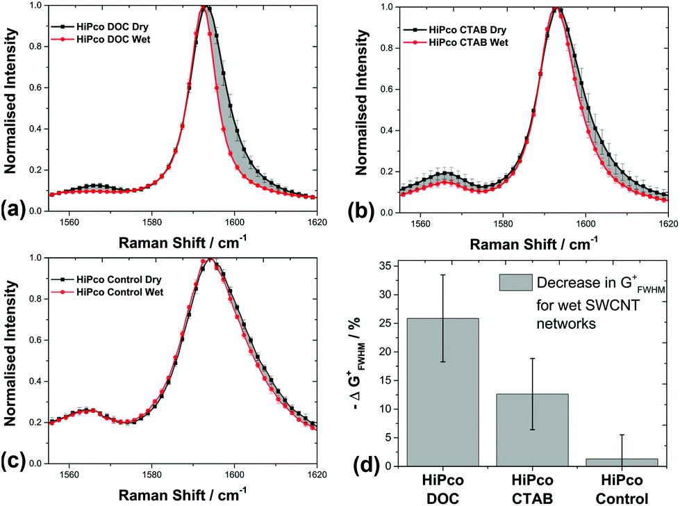 | ||
| Fig. 3 The normalised Raman spectra of dry and wet SWCNT networks containing (a) anionic DOC, (b) cationic CTAB and (c) no surfactant. The differences in line-shape of the G+ (at 1593 cm−1) and G− (at 1565 cm−1) band before and after wetting are highlighted in (a)–(c) by grey shading. The error bars represent the standard deviation between measurements of 3 different spots on the SWCNT film after normalisation of intensity. The percentage decrease in full width at half maximum (FWHM) of the G+ band before and after wetting is shown in (d), where the error bars represent the error on the measurement of the peak FWHM. Raman spectroscopy was performed using a Renshaw inVia Raman microscope with laser wavelength λ = 785 nm and 1 mW power. | ||
In the current study, the decrease in FWHM of the G+ band, along with the suppression of the G−, is treated as a proxy for a change in the gate/charge sensitive G+ band and BWF component respectively. Therefore, the different G-band line-shapes highlighted in Fig. 3 suggest that exposure to water alters the interaction between the charged groups present in the SWCNT-surfactant system. This in turn implies that the electronic properties of SWCNT based devices containing residual surfactant could be altered due to electrostatic interactions upon exposure to water vapour.
Networks of HiPco SWCNTs functionalised with the range of surfactants listed in Table 1 were deposited between gold electrodes and their electrical conductance was recorded in a humidity controlled chamber (described in the Experimental section). The thickness and density of randomly orientated SWCNT films is important when considering gas sensing mechanisms52,53 and charge transport in the network.54 Previous work by Battie et al.55 has shown that SWCNT sensing behaviour changes with a reduction in the number of m-SWCNTs in the film. Randeniya et al.56 found that thinner networks of SWCNTs are more influenced by the substrate. Therefore, surfactant functionalised SWCNT devices based on both thick films (thickness = 19 ± 5 μm, device resistance Rthick = 200 Ω to 500 Ω) and thin films (thickness <1 μm, device resistance Rthin = 50 kΩ to 200 kΩ) were fabricated to investigate how these quantities affect the conductance behaviour in humid conditions.
As is displayed in Fig. 4, the conductance of each network is sensitive to water vapour. At certain time intervals, the relative humidity of the testing chamber is increased and a new steady state conductance value (G) for the network is reached after time t90. The chamber humidity is then reset to 0% and the conductance returns to baseline value (G0).
Fig. 4 and 5 demonstrate that the magnitude and direction of the change in conductance is strongly dependent on the type of surfactant present in the network. When surfactants possessing charged groups are present in the films, the change in conductance is one order of magnitude larger than those without surfactant (the control HiPco SWCNT sample). For the SWCNTs non-covalently functionalised with anionic surfactant (DOC, SC), the conductance decreases upon exposure to water vapour. However, those functionalised with cationic surfactant (CTAB, CTAT) show an increase in conductance when the humidity of the chamber is increased. This is evidence that the head groups and counterions of the ionic surfactants contribute significantly to the electrical properties of the SWCNT networks when exposed to water vapour.
 | ||
| Fig. 4 Real time changes in SWCNT network conductances (where G0 is the baseline conductance at RH = 0% and G is the conductance at higher RH levels) as the relative humidity of the testing chamber is modulated between 0% RH and higher humidity (in the 20% to 70% RH range, as indicated by the top x-axis and blue shaded regions) for thick (thickness = 19 ± 5 μm, dense) networks of (■) HiPco DOC, (●) HiPco SC, (▲) HiPco CTAB, (▼) HiPco CTAT, (+) HiPco Triton X-100 and (★) HiPco control samples. Results for thin (thickness <1 μm, lower-density) networks are plotted without a symbol at the same y-axis offset as their respective sample type. Plots are offset for clarity. | ||
 | ||
| Fig. 5 Magnitude and direction of conductance change for SWCNT network humidity sensors. (a) (■) HiPco CTAB thick (dense) network, (●) HiPco CTAB thin (lower-density) network and (▲) thick HiPco control sample containing no surfactant. (b) (■) HiPco DOC thick (dense) network, (●) HiPco DOC thin (lower-density) network and (▲) thin surfactant free HiPco control sample. The error bars represent the standard deviation of responses from two identical humidity sensors of the same type. | ||
Electrolyte solutions have been utilised to gate SWCNT FETs.22,57 An applied potential causes a re-distribution of charges in the solution, imparting a potential on the nanotubes and causing changes in the intensity, position and line-shape of the SWCNT Raman bands.50 Such changes in the G+ and G− bands are observed for the wetted SWCNT networks containing surfactant in the current study (Fig. 3). The previous use of liquid gated devices, along with the change in line-shape of the G+ and G− bands, indicates that the interaction of the surfactant molecule and counterions with the nanotubes (upon wetting) modulates conduction, effectively gating the SWCNT networks under investigation.
Goak et al.13 proposed that for anionic surfactants such as SC, the Na+ counterion interacts with both m-SWCNTs and sc-SWCNTS electrostatically in dry network films. When such a film is wetted, re-orientation of the surfactant molecules on the surface takes place (in this case the surface of the SWCNTs in the network).58 Therefore, the re-arrangement of the hydrophilic, negatively charged head groups away from the tubes upon wetting would increase the density of positive charges (Na+ for DOC and SC) interacting electrostatically with the nanotubes. This would explain the decrease in conductance through the networks containing residual anionic surfactant.
Conversely, the same re-arrangement of the positively charged, hydrophillic head group for the CTAB containing films would increase the density of Br− counterions interacting with the tubes, inducing a distributed negative charge (δ−) and increasing electron conduction (or decreasing hole density) through the SWCNTs. This proposed mechanism for the respective decrease or increase in conduction for the anionic/cationic surfactant containing films is represented schematically in Fig. 1. The red or blue shifts seen in the SWCNT-surfactant UV-Vis data with respect to the dry samples (Fig. 2, inset), further suggests a change in electrostatic potential, depending on the surfactant–nanotube interaction in water.
Bernardes et al.59 measured a humidity dependent electrostatic potential on the surface of ionic surfactant films, which supports the hypothesis that atmospheric water can change the imparted potential on the SWCNTs in the surfactant containing networks. Additionally, positively charged species (such as the Na+ counterion present in SC and DOC) have previously been found to reduce DC conductance through SWCNTs suspended in liquid water.60
It is not expected that swelling of the surfactant functionalised SWCNT film is solely responsible for the change in network conductance. Although swelling is expected to occur in surfactant films upon exposure to water vapour,61–64 it would always decrease the number of nanotube–nanotube conductive pathways (decreasing film conductance), thus does not account for the increase in conductance of films containing residual cationic agents.
The conductance of the control SWCNT device (containing no surfactant) is also affected by water vapour, although to a lesser extent than the surfactant treated samples. It has been previously reported that water induces n-type65,66 or p-type56,67–69 responses from carbon nanotubes, causing a change in the conductance of ropes and bundles. The study by Bell et al.70 suggested that this effect is attributable to electrostatic interactions. The permanent dipole moment of water induces a polarisation of electronic charge density in the nanotube over a long range (3 nm). Lekawa-Raus et al.71 also suggested that chemical doping does not occur in carbon nanotube fibres, with water vapour instead interacting with the nanotubes at CNT–CNT junctions. If this is the case, then it is to be expected that residual charged species in the network, such as ionic surfactants, increase the polarisation of charge upon exposure to water vapour and thus the magnitude of the conductance change observed in Fig. 5.
Thinner SWCNT networks are increasingly influenced by the substrate and a higher proportion of SWCNTs in the film contribute towards sensing behaviour.56 Furthermore, contact resistance between SWCNTs,24 bundling and electrostatic environment26 influence charge transport in macroscopic networks. In low-density networks of non-sorted SWCNTs below the m-SWCNT perocolation threshold, conductance is increasingly dominated by Schottky barrier modulation at the interface between sc-SWCNT and the electrodes or m-SWCNTs, while thick networks have complete metallic conduction paths with the resistance of the film dominated by nanotube-nanotube junctions.55 Accordingly, the effect of residual surfactant and water vapour was found to differ in thin (and thus lower density) networks.
As a higher proportion of SWCNTs are exposed to the analyte in a thin network, a larger ΔG was expected for thinner SWCNT films. This was the case for the SWCNT control, non-ionic and cationic samples. However, the real time humidity response plots in Fig. 4 show that the opposite is true for thin anionic SWCNT films. Fewer metallic pathways exist in the thinner samples, with the conduction properties of the network increasingly dominated by Schottky barrier modulation between the sc-SWCNTs and m-SWCNTs or the gold electrodes. As chemiresistor type devices are used, there is no applied gate voltage to activate conduction through the sc-SWCNTs in the dry state. However, in a way analogous to electrolyte gated SWCNT transistors, wetting of the film and re-arrangement of surfactant counterions may activate (or reduce, depending on the counterion) conduction through the sc-SWCNTs. Thus, the differences in conductance-humidity behavior of thick vs. thin networks (thickness = 19 ± 5 μm, thickness <1 μm respectively) containing anionic or cationic surfactant may be caused by the increasing influence of the counterion on the sc-SWCNTs in the mixed chirality films.
Reducing the thickness of the SWCNT control sample (surfactant free) switches the direction of the conductive response so that conduction through the network is instead reduced after exposure to water vapour (Fig. 5). Veeramasuneni et al.72 found that an alumina substrate is positively charged at pH 7 upon wetting. If this is the case, the net positive charge may impede electron conduction in the thinner SWCNT control sample, as well as interact with the charged head groups to produce the unexpectedly lower ΔG for the thin network anionic (DOC and SC) samples.
The hot probe method has been applied previously to determine the charge carrier type in sc-SWCNT networks.73 The recorded negative voltage upon probe heating (as shown in Fig. S5 and S6 in the ESI†) indicates that the semiconducting nanotubes in the DOC, CTAB and control (surfactant free) networks are p-type, in line with previous studies of SWCNTs exposed to ambient conditions. The p-type change in potential for the CTAB containing SWCNT network after application of the hot probe (as shown in Fig. S6†) is approximately one order of magnitude lower than the change for the DOC or control network, suggesting the CTAB containing film is less p-type.
As detailed in the ESI,† the setup was adapted so that a segment of the thick (dense) network film could be exposed to water vapour without contacting the hot probe, held at a temperature in the range of 160 °C to 200 °C. The change in potential, firstly due to the application of the hot probe and then due to increasing humidity, was recorded. The potential difference across the DOC containing film increases in magnitude and remains negative when more water vapour is present, whereas the potential across the CTAB film increases in magnitude upon application of the hot probe, but decreases and moves towards a positive value when H2O is introduced (see Fig. S6a and S6b in the ESI†). This indicates that in the CTAB containing networks, exposure to water vapour decreases the p-type behaviour of the sc-SWCNTs in the semiconducting portion of the film. A decrease in the p-type character of sc-SWCNTs would decrease inter-tube resistances between metallic and p-type semiconducting nanotubes, which may explain the overall increase in conductance for the SWCNT-CTAB films upon exposure to water. Correspondingly, the increase in p-type nature of the sc-SWCNTs in the DOC network results in an overall conductance drop, potentially due to increased inter-tube resistances.
When the surfactant containing films are wetted, the current–voltage relationship across the SWCNT network becomes non-linear (as shown in Fig. S8 in the ESI†). It is thought that the counterions impart a partial potential on the SWCNTs in a fashion analogous to electrolyte gating of CNT network FETs. While the Raman bands also display similar changes to line shape observed for electrolyte gated CNT devices,50 further work is required to confirm this hypothesis.
Monitoring of humidity is important for industrial processes, commercial and domestic technologies.74,75 The high sensitivity and reversibility of the SWCNT network conductances upon adsorption and desorption of water vapour indicates that the chemiresistors may be useful as humidity sensors. The conductance-humidity behaviour is predictable and repeatable between multiple identical devices, as shown in Fig. 5, with the chemiresistors containing ionic surfactant functionalised SWCNTs showing the largest ΔG. The percentage change in conductance per percentage change in relative humidity, as displayed in Table 1, compares well with values for carbon nanotube based humidity sensors in the literature (−0.5% RH%−1 from Liu et al.76 and −0.7% RH%−1 by Han et al.77). Some signal drift was observed after exposure to higher levels of relative humidity. This may be addressed by optimising the SWCNT to surfactant ratio and the thickness of the sensing layer.
The devices are low-powered (operating at room temperature), affordable and could be easily incorporated into a sensing array. Furthermore, industrially viable solution based fabrication techniques, such as screen printing or spray coating, could be used for large scale manufacture of such sensors.
4. Conclusions
Conductance through SWCNT networks can be altered via adsorption or desorption of water from the atmosphere. The change in conductance of surfactant containing samples in this study was attributed to the electrostatic interaction of water molecules with the SWCNTs in the network, rather than to chemical doping.Ionic surfactants in the SWCNT films can enhance the change in conductance by a factor of 10. SWCNTs functionalised with cationic surfactants (CTAB and CTAT) demonstrate an increase in conductance upon exposure to water vapour, whereas anionic agents (DOC and SC) have the opposite effect, causing the conductance to decrease. It is suggested that this behaviour is due to the interaction of polar water with the charged head groups and counterions of the ionic surfactants, which impart a partial potential on the SWCNTs.
In line with previous reports, the substrate influences the SWCNT–analyte interaction, enhancing the humidity induced conductance change for thin SWCNT control (surfactant free) networks. Moreover, differences in conductance-humidity behavior of thin vs. thick networks containing anionic or cationic surfactant were attributed to the varying contribution of sc-SWCNTs to conduction across the wetted films.
SWCNT networks functionalised with ionic surfactants display fast and reversible humidity sensing behaviour. Optimising the thickness and type of ionic surfactant may in future enable the development of low powered humidity sensors based on SWCNT networks. Additionally, through investigation of the SWCNT network conductance-humidity behaviour, this study provides a method to evaluate the success of various surfactant removal strategies. The observed intrinsic sensitivity to water vapour demonstrates the importance of assessing the characteristics of SWCNT based devices in humid environments.
Acknowledgements
The authors thank Dr Steve Firth for instrumentation assistance. This work was carried out under EPSRC Grant EP/M506448/1 and EPSRC Grant EP/G037264/1 as part of UCL's Security Science Doctoral Training Centre.References
- B. Liu, C. Wang, J. Liu, Y. Che and C. Zhou, Nanoscale, 2013, 5, 9483–9502 RSC.
- K. Chen, W. Gao, S. Emaminejad, D. Kiriya, H. Ota, H. Y. Y. Nyein, K. Takei and A. Javey, Adv. Mater., 2016, 28, 4397–4414 CrossRef CAS PubMed.
- M. F. L. De Volder, S. H. Tawfick, R. H. Baughman and A. J. Hart, Science, 2013, 339, 535–539 CrossRef CAS PubMed.
- Q. Cao and S. j. Han, Nanoscale, 2013, 5, 8852–8863 RSC.
- E. Penzo, M. Palma, D. A. Chenet, G. Ao, M. Zheng, J. C. Hone and S. J. Wind, ACS Nano, 2016, 10, 2975–2981 CrossRef CAS PubMed.
- S. Park, G. Pitner, G. Giri, J. H. Koo, J. Park, K. Kim, H. Wang, R. Sinclair, H.-S. P. Wong and Z. Bao, Adv. Mater., 2015, 27, 2656–2662 CrossRef CAS PubMed.
- K. Balasubramanian, R. Sordan, M. Burghard and K. Kern, Nano Lett., 2004, 4, 827–830 CrossRef CAS.
- S. B. Yang, B. S. Kong, D. H. Jung, Y.-K. Baek, C.-S. Han, S. K. Oh and H. T. Jung, Nanoscale, 2011, 3, 1361–1373 RSC.
- A. Shimoni, S. Azoubel and S. Magdassi, Nanoscale, 2014, 6, 11084–11089 RSC.
- Z. Wu, Z. Chen, X. Du, J. M. Logan, J. Sippel, M. Nikolou, K. Kamaras, J. R. Reynolds, D. B. Tanner, A. F. Hebard and A. G. Rinzler, Science, 2004, 305, 1273–1276 CrossRef CAS PubMed.
- L. Yu, C. Shearer and J. Shapter, Chem. Rev., 2016, 116, 13413–13453 CrossRef CAS PubMed.
- B. Dan, G. C. Irvin and M. Pasquali, ACS Nano, 2009, 3, 835–843 CrossRef CAS PubMed.
- J. C. Goak, S. H. Lee, J. H. Han, S. H. Jang, K. B. Kim, Y. Seo, Y. S. Seo and N. Lee, Carbon, 2011, 49, 4301–4313 CrossRef CAS.
- M. Chhowalla, J. Soc. Inf. Disp., 2007, 15, 1085–1088 CrossRef CAS.
- J. Li, Y. Lu, Q. Ye, M. Cinke, J. Han and M. Meyyappan, Nano Lett., 2003, 3, 929–933 CrossRef CAS.
- E. S. Snow, F. K. Perkins and J. A. Robinson, Chem. Soc. Rev., 2006, 35, 790 RSC.
- D. Kauffman and A. Star, Angew. Chem., Int. Ed., 2008, 47, 6550–6570 CrossRef CAS PubMed.
- J. M. Schnorr, D. van der Zwaag, J. J. Walish, Y. Weizmann and T. M. Swager, Adv. Funct. Mater., 2013, 5285–5291 CrossRef CAS.
- D. Kumar, P. Chaturvedi, P. Saho, P. Jha, A. Chouksey, M. Lal, J. S. B. S. Rawat, R. P. Tandon and P. K. Chaudhury, Sens. Actuators, B, 2017, 240, 1134–1140 CrossRef CAS.
- G. P. Evans, D. J. Buckley, N. T. Skipper and I. P. Parkin, RSC Adv., 2014, 4, 51395–51403 RSC.
- A. Salehi-Khojin, K. Y. Lin, C. R. Field and R. I. Masel, Nanoscale, 2011, 3, 3097–3102 RSC.
- H. Y. Zheng, O. A. Alsager, B. Zhu, J. Travas-Sejdic, J. M. Hodgkiss and N. O. V. Plank, Nanoscale, 2016, 8, 13659–13668 RSC.
- M. Stadermann, S. J. Papadakis, M. R. Falvo, J. Novak, E. Snow, Q. Fu, J. Liu, Y. Fridman, J. J. Boland, R. Superfine and S. Washburn, Phys. Rev. B: Condens. Matter, 2004, 69, 201402 CrossRef.
- E. Bekyarova, M. E. Itkis, N. Cabrera, B. Zhao, A. Yu, J. Gao and R. C. Haddon, J. Am. Chem. Soc., 2005, 127, 5990–5995 CrossRef CAS PubMed.
- N. Songmee, P. Singjai and M. i. h. Panhuis, Nanoscale, 2010, 2, 1740–1745 RSC.
- P. N. Nirmalraj, P. E. Lyons, S. De, J. N. Coleman and J. J. Boland, Nano Lett., 2009, 9, 3890–3895 CrossRef CAS PubMed.
- A. Saha, C. Jiang and A. A. Martí, Carbon, 2014, 79, 1–18 CrossRef CAS.
- M. C. Hersam, Nat. Nanotechnol., 2008, 3, 387–394 CrossRef CAS PubMed.
- M. S. Arnold, A. A. Green, J. F. Hulvat, S. I. Stupp and M. C. Hersam, Nat. Nanotechnol., 2006, 1, 60–65 CrossRef CAS PubMed.
- S. Ghosh, S. M. Bachilo and R. B. Weisman, Nat. Nanotechnol., 2010, 5, 443–450 CrossRef CAS PubMed.
- J. K. Streit, S. Lam, Y. Piao, A. R. H. Walker, J. A. Fagan and M. Zheng, Nanoscale, 2017, 9, 2531–2540 RSC.
- J. W. Jo, J. W. Jung, J. U. Lee and W. H. Jo, ACS Nano, 2010, 4, 5382–5388 CrossRef CAS PubMed.
- H. Li, J. Zhang, G. Li, F. Tan, R. Liu, R. Li, T. Zhang, H. Jin and Q. Li, Carbon, 2014, 66, 369–376 CrossRef CAS.
- A. Abdelhalim, A. Abdellah, G. Scarpa and P. Lugli, Carbon, 2013, 61, 72–79 CrossRef CAS.
- M. Shimizu, S. Fujii, T. Tanaka and H. Kataura, J. Phys. Chem. C, 2013, 117, 11744–11749 CAS.
- H. Z. Geng, D. S. Lee, K. K. Kim, G. H. Han, H. K. Park and Y. H. Lee, Chem. Phys. Lett., 2008, 455, 275–278 CrossRef CAS.
- J. Tittmann-Otto, S. Hermann, J. Kalbacova, M. Hartmann, M. Toader, R. D. Rodriguez, S. E. Schulz, D. R. T. Zahn and T. Gessner, J. Appl. Phys., 2016, 119, 124509 CrossRef.
- A. A. Kane, A. C. Ford, A. Nissen, K. L. Krafcik and F. Léonard, ACS Nano, 2014, 8, 2477–2485 CrossRef CAS PubMed.
- J. G. Park, J. Smithyman, C. Y. Lin, A. Cooke, A. W. Kismarahardja, S. Li, R. Liang, J. S. Brooks, C. Zhang and B. Wang, J. Appl. Phys., 2009, 106, 104310 CrossRef.
- H. Z. Geng, K. K. Kim, K. P. So, Y. S. Lee, Y. Chang and Y. H. Lee, J. Am. Chem. Soc., 2007, 129, 7758–7759 CrossRef CAS PubMed.
- D. S. Hecht, D. Thomas, L. Hu, C. Ladous, T. Lam, Y. Park, G. Irvin and P. Drzaic, J. Soc. Inf. Disp., 2009, 17, 941–946 CrossRef CAS.
- G. P. Evans, D. J. Buckley, A. L. Adedigba, G. Sankar, N. T. Skipper and I. P. Parkin, ACS Appl. Mater. Interfaces, 2016, 8, 28096–28104 CAS.
- P. Nikolaev, M. J. Bronikowski, R. K. Bradley, F. Rohmund, D. T. Colbert, K. A. Smith and R. E. Smalley, Chem. Phys. Lett., 1999, 313, 91–97 CrossRef CAS.
- G. Golan, A. Axelevitch, B. Gorenstein and V. Manevych, Microelectron. J., 2006, 37, 910–915 CrossRef CAS.
- S. C. Naisbitt, K. F. E. Pratt, D. E. Williams and I. P. Parkin, Sens. Actuators, B, 2006, 114, 969–977 CrossRef CAS.
- Y. R. Park, W. J. Kim, M. J. Ko, N. K. Min and C. J. Lee, Nanoscale, 2012, 4, 6532–6536 RSC.
- I. W. Chiang, B. E. Brinson, A. Y. Huang, P. A. Willis, M. J. Bronikowski, J. L. Margrave, R. E. Smalley and R. H. Hauge, J. Phys. Chem. B, 2001, 105, 8297–8301 CrossRef CAS.
- J. L. Blackburn, C. Engtrakul, T. J. McDonald, A. C. Dillon and M. J. Heben, J. Phys. Chem. B, 2006, 110, 25551–25558 CrossRef CAS PubMed.
- M. S. Dresselhaus, G. Dresselhaus, R. Saito and A. Jorio, Phys. Rep., 2005, 409, 47–99 CrossRef.
- J. Zaumseil, F. Jakubka, M. Wang and F. Gannott, J. Phys. Chem. C, 2013, 117, 26361–26370 CAS.
- G. Fanchini, H. E. Unalan and M. Chhowalla, Nano Lett., 2007, 7, 1129–1133 CrossRef CAS PubMed.
- A. Boyd, I. Dube, G. Fedorov, M. Paranjape and P. Barbara, Carbon, 2014, 69, 417–423 CrossRef CAS.
- A. Salehi-Khojin, F. Khalili-Araghi, M. A. Kuroda, K. Y. Lin, J. P. Leburton and R. I. Masel, ACS Nano, 2011, 5, 153–158 CrossRef CAS PubMed.
- V. Skákalová, A. B. Kaiser, Y. S. Woo and S. Roth, Phys. Rev. B: Condens. Matter, 2006, 74, 085403 CrossRef.
- Y. Battie, L. Gorintin, O. Ducloux, P. Thobois, P. Bondavalli, G. Feugnet and A. Loiseau, Analyst, 2012, 137, 2151–2157 RSC.
- L. K. Randeniya and P. J. Martin, Carbon, 2013, 60, 498–505 CrossRef CAS.
- S. Rosenblatt, Y. Yaish, J. Park, J. Gore, V. Sazonova and P. L. McEuen, Nano Lett., 2002, 2, 869–872 CrossRef CAS.
- K. H. S. Kung and K. F. Hayes, Langmuir, 1993, 9, 263–267 CrossRef CAS.
- J. S. Bernardes, C. A. Rezende and F. Galembeck, J. Phys. Chem. C, 2010, 114, 19016–19023 CAS.
- B. H. Son, J.-Y. Park, S. Lee and Y. H. Ahn, Nanoscale, 2015, 7, 15421–15426 RSC.
- D. Grosso, F. Cagnol, G. J. de. A. A. Soler-Illia, E. L. Crepaldi, H. Amenitsch, A. Brunet-Bruneau, A. Bourgeois and C. Sanchez, Adv. Funct. Mater., 2004, 14, 309–322 CrossRef CAS.
- J. S. Bernardes, C. A. Rezende and F. Galembeck, Langmuir, 2010, 26, 7824–7832 CrossRef CAS PubMed.
- S. Björklund and V. Kocherbitov, Langmuir, 2016, 32, 5223–5232 CrossRef PubMed.
- Y. L. E. Chen, M. L. Gee, C. A. Helm, J. N. Israelachvili and P. M. McGuiggan, J. Phys. Chem., 1989, 93, 7057–7059 CrossRef CAS.
- A. Zahab, L. Spina, P. Poncharal and C. Marlière, Phys. Rev. B: Condens. Matter, 2000, 62, 10000–10003 CrossRef CAS.
- D. Tang, L. Ci, W. Zhou and S. Xie, Carbon, 2006, 44, 2155–2159 CrossRef CAS.
- D. Jung, J. Kim and G. S. Lee, Sens. Actuators, A, 2015, 223, 11–17 CrossRef CAS.
- C. Cantalini, L. Valentini, I. Armentano, L. Lozzi, J. M. Kenny and S. Santucci, Sens. Actuators, B, 2003, 95, 195–202 CrossRef CAS.
- H. E. Romero, G. U. Sumanasekera, S. Kishore and P. C. Eklund, J. Phys.: Condens. Matter, 2004, 16, 1939 CrossRef CAS.
- R. A. Bell, M. C. Payne and A. A. Mostofi, J. Chem. Phys., 2014, 141, 164703 CrossRef PubMed.
- A. Lekawa-Raus, L. Kurzepa, G. Kozlowski, S. C. Hopkins, M. Wozniak, D. Lukawski, B. A. Glowacki and K. K. Koziol, Carbon, 2015, 87, 18–28 CrossRef CAS.
- S. Veeramasuneni, M. R. Yalamanchili and J. D. Miller, J. Colloid Interface Sci., 1996, 184, 594–600 CrossRef CAS PubMed.
- M. Piao, M. K. Joo, J. Na, Y. J. Kim, M. Mouis, G. Ghibaudo, S. Roth, W. Y. Kim, H. K. Jang, G. P. Kennedy, U. Dettlaff-Weglikowska and G. T. Kim, J. Phys. Chem. C, 2014, 118, 26454–26461 CAS.
- T. A. Blank, L. P. Eksperiandova and K. N. Belikov, Sens. Actuators, B, 2016, 228, 416–442 CrossRef CAS.
- Q. Y. Tang, Y. C. Chan and K. Zhang, Sens. Actuators, B, 2011, 152, 99–106 CrossRef CAS.
- L. Liu, X. Ye, K. Wu, R. Han, Z. Zhou and T. Cui, Sensors, 2009, 9, 1714–1721 CrossRef CAS PubMed.
- J. W. Han, B. Kim, J. Li and M. Meyyappan, J. Phys. Chem. C, 2012, 116, 22094–22097 CAS.
Footnote |
| † Electronic supplementary information (ESI) available. See DOI: 10.1039/C7NR02141K |
| This journal is © The Royal Society of Chemistry 2017 |