
 Open Access Article
 This Open Access Article is licensed under a
 Creative Commons Attribution 3.0 Unported Licence
Reconfigurable optical manipulation by phase change material waveguides†
Tianhang
Zhang‡
 *ab,
Shengtao
Mei‡
ab,
Qian
Wang
c,
Hong
Liu
c,
Chwee Teck
Lim
ad and
Jinghua
Teng
c
*ab,
Shengtao
Mei‡
ab,
Qian
Wang
c,
Hong
Liu
c,
Chwee Teck
Lim
ad and
Jinghua
Teng
c
aGraduate School for Integrative Sciences and Engineering, National University of Singapore, Centre for Life Sciences (CeLS), #05-01, 28 Medical Drive, Singapore 117456. E-mail: a0113469@u.nus.edu
bDepartment of Electrical and Computer Engineering, National University of Singapore, 4 Engineering Drive 3, Singapore 117583
cInstitute of Materials Research and Engineering Agency for Science Technology and Research (A*STAR), #08-03, 2 Fusionopolis Way, Innovis, Singapore 138634
dDepartment of Biomedical Engineering, National University of Singapore, 4 Engineering Drive 3, Singapore 117583
First published on 25th April 2017
Abstract
Optical manipulation by dielectric waveguides enables the transportation of particles and biomolecules beyond diffraction limits. However, traditional dielectric waveguides could only transport objects in the forward direction which does not fulfill the requirements of the next generation lab-on-chip system where the integrated manipulation system should be much more flexible and multifunctional. In this work, bidirectional transportation of objects on the nanoscale is demonstrated on a rectangular waveguide made of the phase change material Ge2Sb2Te5 (GST) by numerical simulations. Either continuous pushing forces or pulling forces are generated on the trapped particles when the GST is in the amorphous or crystalline phase. With the technique of a femtosecond laser induced phase transition on the GST, we further proposed a reconfigurable optical trap array on the same waveguide. This work demonstrates GST waveguide's potential of achieving multifunctional manipulation of multiple objects on the nanoscale with plausible optical setups.
1. Introduction
Since the invention of optical tweezers1 in the 1970s, they have been developed into a powerful tool to manipulate micro-objects and bio-molecules. The trapping by optical tweezers is based on the gradient force whose direction and magnitude are proportional to the local field gradient. In order to trap multiple objects at different positions, acousto-optic technology2 and holographic technology3 are combined with optical tweezers to generate multiple optical traps or optical trap arrays. The trapping positions of holographic optical tweezers could be reconfigured by programming the spatial light modulator to shape the incident light, thus generating the desired field pattern at the target plane. Meanwhile, the study of radiation pressure which is owing to the transfer of momentum from the light to the illuminated objects has also become popular in recent years. Non-diffraction beams which could maintain their transverse intensity profiles during the propagation such as Bessel beam and Airy beam have been used to transport objects in the long range by the radiation pressure.4,5 Intuitively, the radiation pressure should always push the objects in the beam propagating direction. Recent advances have taken advantages of non-paraxial structured beams to pull instead of pushing the objects towards the light source, i.e. optical tractor beams.6–8The manipulated objects’ size of either optical tweezers or non-diffraction beams is limited to the micrometer scale due to the diffraction limits. In order to manipulate sub-wavelength objects, optical forces generated by dielectric nanostructures such as waveguides,9 slot waveguides10 and waveguide loops11 have become a popular topic. Such waveguide structures generate an exponential decayed electric field within an area beyond the diffraction limits which traps particles on the nanometer scale to waveguide surfaces and transports them by the propagation fields. Another merit of manipulation by waveguides is that transporting objects in a certain trajectory could be much more easily implemented by designing waveguides in the desired shape than by controlling the propagating path of a laser beam. Usually, dielectric waveguides are designed with single manipulation function: transporting particles in the forward direction. Only very recently, transporting particles by waveguides opposite to the field-propagating direction has been proposed in the far infrared range.12 When the injected light is below the cutoff frequency, the propagating mode is turned into the evanescent mode in which the field intensity decays along the propagating direction. Under the evanescent mode, the gradient force overcomes the radiation pressure on the particles and pulls the particles towards the light source. However, under different wavelengths, the calculated pushing force (∼4 × 10⁻²⁷ N) is 8 orders smaller than the pulling force (∼6 × 10⁻¹⁹ N). Such a small pushing force is very difficult to demonstrate in practice. The next generation ‘lab-on-chip’ system13–15 combines optical manipulation, microfluidic and other techniques to enable multifunctional devices that could do multiple cells manipulation and analysis on a single chip. Such a system requires tunable and multifunctional manipulation tools which could be able to trap and transport objects freely between areas.
The chalcogenide compound GST is famous for its applications in rewritable optical discs and phase-change memory.16 Usually, the phase switching of GST can be achieved by nanosecond and microsecond laser heating: the amorphous GST will be crystallized when it is heated between its crystallization temperature and melting temperature, while a high density laser pulse will melt the crystalline GST to its amorphous phase. The rapid phase transition rate of GST enables a number of applications in tunable and reconfigurable devices. Wang et al. have demonstrated a femtosecond laser induced bidirectional phase transition in a volume resolution as small as 0.02 μm3 and two-dimensional reconfigurable functional patterns with the writing technique.17
In this paper, we proposed a multifunctional device based on a single rectangular waveguide made of GST. The waveguide could generate continuous pushing or pulling force with the same order of magnitude over a distance of more than 10 μm on gold particles (diameter = 50 nm) when the GST is in the amorphous phase or crystalline phase respectively at a working wavelength of 1.75 μm. Benefitting from the femtosecond laser writing technique,17 we further demonstrated a reconfigurable optical trap array on the GST waveguide which could trap small particles at pre-designed regions. By switching a certain region of the amorphous phase GST waveguide to the crystalline phase by using a femtosecond laser, small particles could be trapped at the junction of amorphous and crystalline regions. Such a trapping pattern could be erased by using the same femtosecond laser with different configurations, making the whole process reconfigurable. Thus, only simple modifications of a single waveguide are needed to realize the following two functions: (1) transporting the particles in the positive/negative direction; (2) trapping the particles at the desired regions which mimic the function of optical pushing/pulling by non-diffraction beams and optical trap arrays respectively but with the potential to manipulate objects on the nanometer scale.
2. Results and discussion
2.1 Switchable push–pull particle manipulation of the GST waveguide
Non-diffraction beams which trap the illuminated objects towards their beam center and transport them along the beam propagating direction by radiation pressure show advantages in simultaneous and long range manipulation. The invention of optical tractor beams has enhanced the degree of freedom of manipulation and opened up the gate to a myriad of novel manipulation applications such as optical sorting18 and long range bidirectional transportation.19 On the other hand, the optical tractor beams need the close interplay between the incident beams and illuminated objects which require the objects’ sizes to be within a certain range and the illuminating beams’ profile to be complex.20 In the following, we will show by using a simple nanostructure of a single waveguide made of GST, continuous optical pushing force could be generated on gold particles of 50 nm diameter size for over 10 μm distance. Switching the phase of the GST material from amorphous to crystalline by heating the structure to above GST's crystallization temperature, the pushing force will be turned into pulling force. Switching GST's phase back to amorphous by heating the structure to above its melting temperature, the pulling force will be turned into pushing force again.The structure we considered is a GST rectangular waveguide with a width of 800 nm and a height of 500 nm deposited on a SiO2 substrate as shown in Fig. 1a. The refractive index of GST in the amorphous phase and crystalline phase is plotted in Fig. 1b and c. A significant contrast could be found between the two phases: above the wavelength of 1.75 μm, a pronounced difference could be seen in both the real parts and the imaginary parts of the refractive index. In this wavelength range, the crystalline phase GST suffers from heavy losses while the amorphous phase GST has almost zero losses. Due to such contrast, the propagating mode could be turned into a decaying mode when switching its phase from amorphous to crystalline. The electric field magnitude for the Transverse Magnetic (TM) mode above the top surface is plotted for propagating mode and decaying mode as shown in Fig. 2a. The propagating mode maintains a relatively constant intensity along the beam propagating direction while the field decays exponentially for the decaying mode. The electric field intensity over the waveguide cross-section is plotted in Fig. 2b. The area with the highest field intensity above the waveguide can be treated as the ‘hotspot’ which traps the nanoparticles in the y–z plane (details shown in the ESI†), while the particles are transported by the field in the x direction.
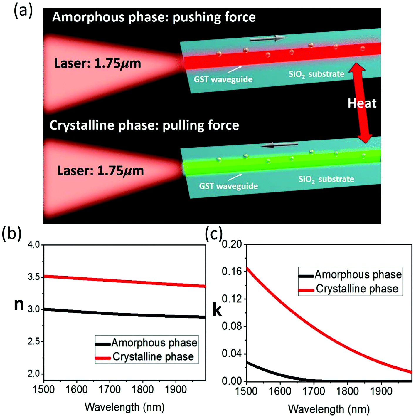 | ||
| Fig. 1 (a) Schematic of push/pull manipulation of nanoparticles by the GST waveguide. Laser with a wavelength of 1.75 μm is injected into the GST waveguide of 800 nm × 500 nm fabricated above the SiO2 substrate. When the waveguide is in the amorphous phase, the generated field exerts continuous pushing force on gold nanoparticles. When the waveguide is in the crystalline phase, the force is pulling. (b) The real part and (c) imaginary part of the refractive index of the GST material. Above the wavelength of 1.75 μm, the crystalline phase GST suffers from heavy losses, causing the optical field decaying during the propagating in the waveguide. | ||
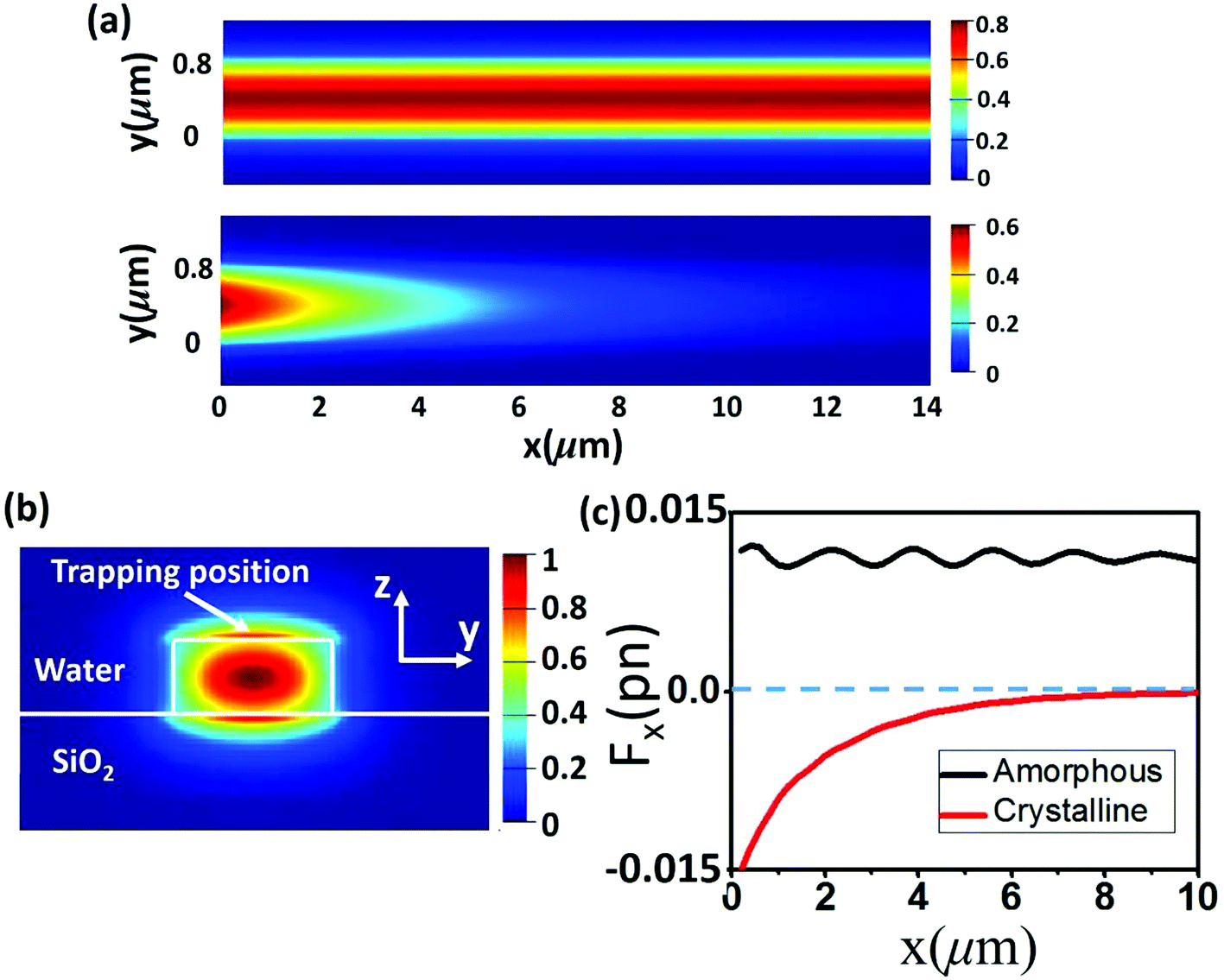 | ||
| Fig. 2 (a) Electric field of propagating mode when the waveguide is in the amorphous phase and decaying mode when the waveguide is in the crystalline phase. (b) Electric field of the cross section. TM mode is considered and the nanoparticle is trapped above the waveguide where the field intensity is strongest. (c) Optical force on 50 nm gold particles when the waveguide is in the amorphous phase and crystalline phase under 100 mW incident power. Continuous pushing force is switched to pulling forces when the GST material is switched from the amorphous phase to the crystalline phase. | ||
For a nanoparticle trapped above the top surface, two kinds of optical forces are considered in the x direction: the gradient force and the radiation pressure. Under propagating mode, the field is almost gradientless in the propagating direction, thus the gradient force vanishes and only radiation pressure exists. Such radiation pressure pushes the nanoparticle towards the field propagating direction. Under decaying mode, gradient force and radiation pressure both exist while the gradient force dominates due to the fast decaying rate of the field. Such gradient force pulls the particles to the area with the highest intensity i.e. the light source.
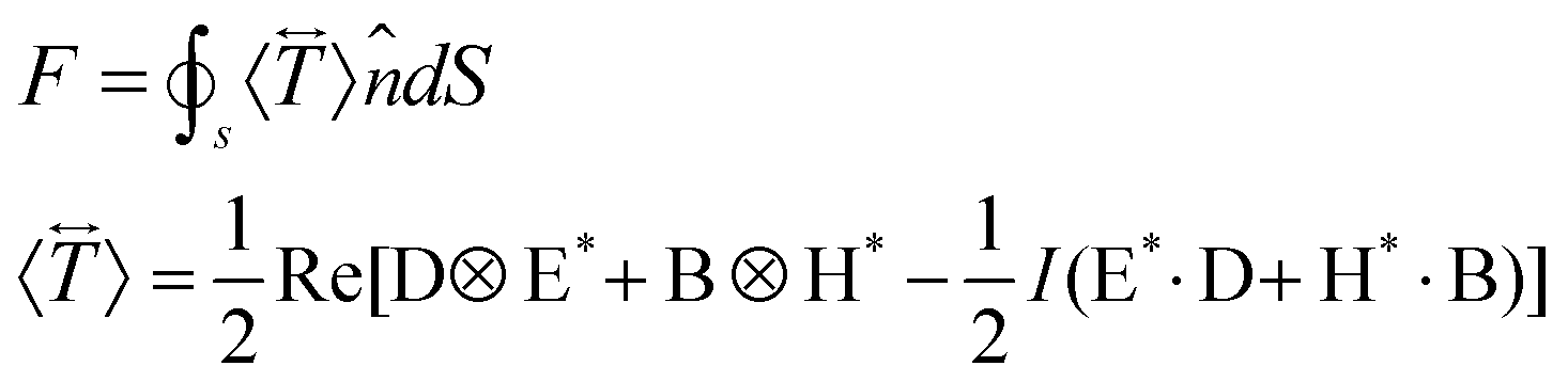
To verify the above pushing and pulling forces, full wave simulation is conducted by the Finite Difference Time Domain (FDTD) method using a commercial software (Lumerical FDTD Solutions). A 50 nm gold particle is placed 30 nm above the waveguide top surface in the medium of water and the time averaged optical force is calculated by integrating the Maxwell Stress Tensor
 | (1) |
2.2 Reconfigurable optical traps based on the GST waveguide
In the previous section, we have demonstrated the continuous bidirectional transportation of nanoparticles when the whole waveguide is in the amorphous phase or crystalline phase. The advance of the femtosecond laser induced GST phase transition enables us to switch the phase within a very small region instead of switching the whole waveguide. In the following, we will show that the nanostructure discussed in the last section can be used to trap nanoparticles at pre-defined regions when introducing certain small-area phase inhomogeneity to the waveguide. As shown in Fig. 3a, when a certain region of an amorphous phase GST waveguide is switched to the crystalline phase, in the x direction, nanoparticles could be trapped near the junction between these two regions. The waveguide is in the same dimension with the one described in the previous section. The laser with a wavelength of 1.75 μm is injected from the region with the amorphous phase in the Transverse Electric (TE) mode. Since the region of the crystalline phase next to the amorphous region has a different refractive index, some reflection exists in the propagating field. In the current design, the length of the crystalline region is set to 330 nm to minimize these reflections. As can be seen from the electric fields with single or double crystalline phase regions on an amorphous phase waveguide (Fig. 3b and c), the field intensity drops abruptly at the junction of the amorphous region and the crystalline region while it restores to almost 90% of the original value when it continues to propagate in the next amorphous region. The field decaying is very limited, thus several crystalline regions could be written on the same waveguide which enables an optical trap array. In the full picture, the crystalline regions behave like ‘defects’ in the whole waveguide which causes large oscillations of the field. Within the crystalline regions, the field oscillations generate large restoring forces on nanoparticles which could trap these particles at those regions. After passing through the crystalline regions, the field propagates with relatively constant intensity which generates radiation pressure dominated optical forces that push the particles in the field propagating direction. The distance between the different crystalline regions could be designed to fulfill different tasks.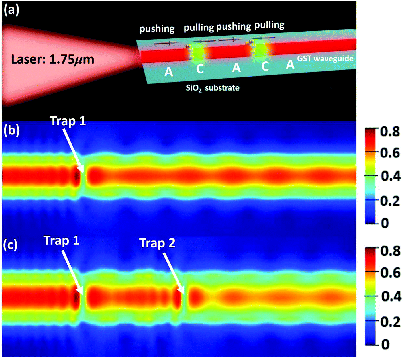 | ||
| Fig. 3 (a) Schematic of reconfigurable optical waveguide traps. Originally the whole waveguide is made of amorphous phase GST. Then the predefined trapping regions (green region) are phase switched from amorphous to crystalline by using a femtosecond laser. When a 1.75 μm laser is injected into the waveguide, the nanoparticles are trapped at the junction between the amorphous phase region and the crystalline phase region. (b) Electric field above the waveguide when one and (c) two trapping regions are defined. | ||
To demonstrate the trapping function of the device, the optical forces on 50 nm gold particles in single or double optical traps are calculated using the same method of the Maxwell stress tensor in the previous section and plotted against its positions along the waveguide in Fig. 4a and c. Continuous pushing forces in the amorphous phase region could transport particles towards the crystalline region and large restoring forces trap these particles near the junction of the amorphous region and the crystalline region. The major trapping positions are marked in Fig. 4a and c where the restoring force stiffness is maximum. Although some small turbulence of optical force exists in the amorphous region due to the reflections mentioned above, the force always pushes the particles towards the next trapping region. To illustrate the trapping more intuitively, we calculated the potential along the waveguide by integrating the optical force21 . One or two potential wells of around 4 kT are derived for waveguides with single or double traps as shown in Fig. 4b and d. In the amorphous regions, the potential continuously goes lower, which transports the particles to these potential wells and the potential wells could trap the particles at the local potential minimum. These potential wells could be written in the waveguide by femtosecond laser induced phase transitions from amorphous to crystalline. When a new trapping array with different numbers of traps or distance between traps is needed, the crystalline regions could be easily erased by using the same femtosecond laser with different configurations. Such writing and erasing processes make the whole device reconfigurable subject to different designs.
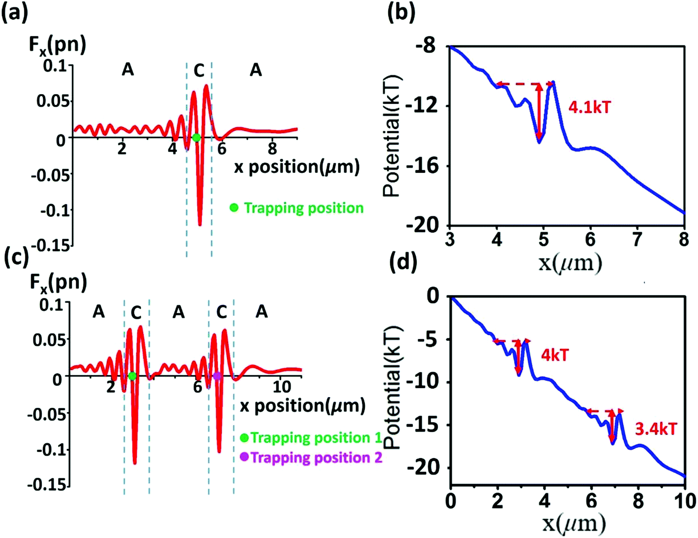 | ||
| Fig. 4 Simulated optical force on 50 nm gold particles in the x direction in GST optical waveguide traps with (a) one and (c) two predefined trapping positions. (b) and (d) Calculated potentials for these two cases under 100 mW incident power. | ||
3. Conclusions
In conclusion, we have demonstrated a novel optical manipulation platform based on a single waveguide made of the phase change material GST. Compared with the conventional waveguide which could only push objects in the forward direction, our device is able to pull objects backward and the switching between push and pull can be simply realized by switching the phase of GST. Besides this, the device also integrates the function of reconfigurable trapping nanoparticles at multiple predefined regions. This work may inspire new applications of simultaneous trapping and transporting multiple nanoparticles/molecules in fundamental physics and biology studies.Conflict of interest
The authors declare no competing financial interest.References
- A. Ashkin, J. Dziedzic, J. Bjorkholm and S. Chu, Opt. Lett., 1986, 11, 288–290 CrossRef CAS PubMed.
- K. Visscher, S. P. Gross and S. M. Block, IEEE J. Sel. Top. Quantum Electron., 1996, 2, 1066–1076 CrossRef CAS.
- J. E. Curtis, B. A. Koss and D. G. Grier, Opt. Commun., 2002, 207, 169–175 CrossRef CAS.
- J. Arlt, V. Garces-Chavez, W. Sibbett and K. Dholakia, Opt. Commun., 2001, 197, 239–245 CrossRef CAS.
- V. Garces-Chavez, D. McGloin, H. Melville, W. Sibbett and K. Dholakia, Nature, 2002, 419, 145–147 CrossRef CAS PubMed.
- A. Novitsky, C. W. Qiu and H. F. Wang, Phys. Rev. Lett., 2011, 107 CrossRef CAS PubMed , 203601.
- J. Chen, J. Ng, Z. F. Lin and C. T. Chan, Nat. Photonics, 2011, 5, 531–534 CrossRef CAS.
- S. Sukhov and A. Dogariu, Phys. Rev. Lett., 2011, 107 CrossRef CAS PubMed , 203602.
- S. Kawata and T. Tani, Opt. Lett., 1996, 21, 1768–1770 CrossRef CAS PubMed.
- A. H. Yang, S. D. Moore, B. S. Schmidt, M. Klug, M. Lipson and D. Erickson, Nature, 2009, 457, 71–75 CrossRef CAS PubMed.
- O. G. Hellesø, P. Løvhaugen, A. Z. Subramanian, J. S. Wilkinson and B. S. Ahluwalia, Lab Chip, 2012, 12, 3436–3440 RSC.
- N. K. Paul and B. A. Kemp, Prog. Electromagn. Res., 2015, 151, 73–81 CrossRef.
- R. Burger, D. Kurzbuch, R. Gorkin, G. Kijanka, M. Glynn, C. McDonagh and J. Ducree, Lab Chip, 2015, 15, 378–381 RSC.
- M. Esseling, B. Kemper, M. Antkowiak, D. J. Stevenson, L. Chaudet, M. A. Neil, P. W. French, G. von Bally, K. Dholakia and C. Denz, J. Biophotonics, 2012, 5, 9–13 CrossRef CAS PubMed.
- M. Soltani, J. Lin, R. A. Forties, J. T. Inman, S. N. Saraf, R. M. Fulbright, M. Lipson and M. D. Wang, Nat. Nanotechnol., 2014, 9, 448–452 CrossRef CAS PubMed.
- B. J. Eggleton, B. Luther-Davies and K. Richardson, Nat. Photonics, 2011, 5, 141–148 CAS.
- Q. Wang, E. T. Rogers, B. Gholipour, C.-M. Wang, G. Yuan, J. Teng and N. I. Zheludev, Nat. Photonics, 2016, 10, 60–65 CrossRef CAS.
- O. Brzobohaty, V. Karasek, M. Siler, L. Chvatal, T. Cizmar and P. Zemanek, Nat. Photonics, 2013, 7, 123–127 CrossRef CAS.
- V. Shvedov, A. R. Davoyan, C. Hnatovsky, N. Engheta and W. Krolikowski, Nat. Photonics, 2014, 8, 846–850 CrossRef CAS.
- A. Novitsky, C.-W. Qiu and A. Lavrinenko, Phys. Rev. Lett., 2012, 109, 023902 CrossRef PubMed.
- L. Novotny, R. X. Bian and X. S. Xie, Phys. Rev. Lett., 1997, 79, 645–648 CrossRef CAS.
Footnotes |
| † Electronic supplementary information (ESI) available. See DOI: 10.1039/c7nr00876g |
| ‡ These authors contributed equally to this work. |
| This journal is © The Royal Society of Chemistry 2017 |