
 Open Access Article
 This Open Access Article is licensed under a
 Creative Commons Attribution 3.0 Unported Licence
Towards higher electron mobility in modulation doped GaAs/AlGaAs core shell nanowires†
Jessica L.
Boland
a,
Gözde
Tütüncüoglu
b,
Juliane Q.
Gong
a,
Sonia
Conesa-Boj
c,
Christopher L.
Davies
a,
Laura M.
Herz
 a,
Anna
Fontcuberta i Morral
b and
Michael B.
Johnston
*a
a,
Anna
Fontcuberta i Morral
b and
Michael B.
Johnston
*a
aDepartment of Physics, University of Oxford, Clarendon Laboratory, Parks Road, Oxford, OX1 3PU, UK. E-mail: michael.johnston@physics.ox.ac.uk
bLaboratory of Semiconductor Materials, École polytechnique fédérale de Lausanne (EPFL), CH-1015 Lausanne, Switzerland
cKavli Institute of Nanoscience, Delft, University of Technology Lorentzweg 1, 2628 CJ Delft, The Netherlands
First published on 17th May 2017
Abstract
Precise control over the electrical conductivity of semiconductor nanowires is a crucial prerequisite for implementation of these nanostructures into novel electronic and optoelectronic devices. Advances in our understanding of doping mechanisms in nanowires and their influence on electron mobility and radiative efficiency are urgently required. Here, we investigate the electronic properties of n-type modulation doped GaAs/AlGaAs nanowires via optical pump terahertz (THz) probe spectroscopy and photoluminescence spectroscopy over the temperature range 5 K–300 K. We directly determine an ionization energy of 6.7 ± 0.5 meV (T = 52 K) for the Si donors within the AlGaAs shell that create the modulation doping structure. We further elucidate the temperature dependence of the electron mobility, photoconductivity lifetime and radiative efficiency, and determine the charge-carrier scattering mechanisms that limit electron mobility. We show that below the donor ionization temperature, charge scattering is limited by interactions with interfaces, leading to an excellent electron mobility of 4360 ± 380 cm2 V−1 s−1 at 5 K. Above the ionization temperature, polar scattering via longitudinal optical (LO) phonons dominates, leading to a room temperature mobility of 2220 ± 130 cm2 V−1 s−1. In addition, we show that the Si donors effectively passivate interfacial trap states in the nanowires, leading to prolonged photoconductivity lifetimes with increasing temperature, accompanied by an enhanced radiative efficiency that exceeds 10% at room temperature.
1. Introduction
Semiconductor nanowires are of increasing interest in the field of nanotechnology, owing to their suitability for high-speed, electronic and optoelectronic devices.1 Their unique, one-dimensional nature allows for the realisation of lattice-matched axial and radial heterostructures, which have the potential for direct integration into silicon-based devices. To date, many optoelectronic devices based on these nanowire heterostructures have already been demonstrated, such as nanowire solar cells,2–5 field effect transistors,6–8 room temperature lasers,9–11 light emitting diodes12–14 and terahertz (THz) detectors.15–18 In order to further develop these devices, control of the nanowire conductivity is essential. One way of achieving such control is to dope the nanowire with impurity ions to tailor transport properties, such as carrier mobility and lifetime.In the past decade, research into electrically doping semiconductor nanowires has increased rapidly, following the demonstration of doped silicon nanowires.19 Doping was first investigated over three decades ago with the development of p–n junctions in GaAs nanowires20 and since then, both n-type and p-type doping within the nanowire core and shell respectively have been realised.21–28
Nanowire devices based on Group III–V semiconductors show particular promise, owing to high electron mobilities and the ability to engineer the bandgaps of III–V materials. However, there are two key challenges to be addressed before the precise and reproducible control of electrical doping required for many NW device applications is realised. Firstly, the inclusion of dopants often leads to ineffective and/or inhomogeneous doping,29–34 and secondly, doping can lead to a severe reduction in the electrical mobility of nanowires, owing to impurity scattering.28,35,36
The technique of modulation doping is an excellent solution to these problems and has been implemented extensively in high mobility semiconductor devices with planar heterostructure architectures.37,38 By spatially separating the ionised impurities from the free charge carriers, impurity scattering can be reduced and a high carrier mobility obtained. Recently, modulation doping in semiconductor nanowire hetereostructures has been demonstrated and shown to produce high extrinsic carrier concentrations with minimal degradation of the carrier mobility, making them appealing for extensive study.27,39,40 For example, modulation doped InAs/InP41 and GaAs/AlGaAs42 nanowires have exhibited room-temperature mobilities of 2000 cm2 V−1 s−1 and 2200 cm2 V−1 s−1 respectively; and GaAs/AlGaAs nanowires have also been recently implemented into NW-FETs.8 From these results, it is apparent that modulation doping is an effective way of controlling the nanowire conductivity, however the electron mobility is still lower than for planar devices.37,38
So the question remain, as to what underlying mechanisms limit charge conductivity and mobility in modulation-doped nanowires. To this end, a fundamental understanding of dopant ionisation and charge scattering is needed. However, utilising conventional temperature-dependent Hall techniques on nanowires to investigate these properties is difficult, as fabricating lateral electrical contacts onto the nanowire is challenging and accurate doping concentrations are hard to extract.43 In contrast, the technique of THz spectroscopy offers an effective method of characterising the electrical properties of nanowires in a non-contact fashion. By measuring the transport properties of the modulation-doped nanowires as a function of temperature, the mechanisms of charge-carrier scattering may then be elucidated.
In this work, we determine the scattering mechanisms that limit electron mobility in modulation-doped GaAs/AlGaAs nanowires using temperature-dependent THz conductivity spectroscopy. Furthermore, we measure the ionisation energy of Si donors in these NWs to be 6.72 ± 0.52 meV. Significantly, we demonstrate an increase in carrier mobility at low temperatures, reaching ∼4500 cm2 V−1 s−1 at 5 K. Fitting of the mobilities as a function of temperature for the modulation doped sample shows that for temperatures above 50 K, scattering from LO phonons mainly governs the carrier mobility, with modulation doping suppressing interface and impurity scattering. Furthermore, we observe an increase in radiative efficiency for temperatures above the donor ionisation temperature, reaching a radiative efficiency of ∼10% at room temperature. Surprisingly, this increase in radiative efficiency was accompanied by a clear increase in carrier lifetime, from 0.81 ns to 2.13 ns. While an increase in radiative lifetime is usually associated with a reduction in charge carrier lifetime, we attribute these results to ionised electrons passivating trap states at the core–shell interface.
2. Experimental details
Core–shell GaAs/Al0.33Ga0.67As nanowires were grown via molecular beam epitaxy (MBE) on a p-type (111) Si substrate. Growth conditions were optimised to maximise nanowire yield and details can be found in the ESI.† After forming the GaAs nanowire core, growth parameters were changed to obtain a larger bandgap Al0.33Ga0.67As shell. After a period of time after growth of the AlGaAs shell, Si impurities were then introduced to produce a n-type delta-doped layer at a distance of 12 nm away from the GaAs/AlGaAs interface with a nominal doping density of ND = 4.5 ± 0.5 × 1018 cm−3. Growth of the AlGaAs shell without the Si impurities was then continued and a thin GaAs capping layer coated on top of this shell to limit oxidation. Modulation-doped core–shell GaAs/AlGaAs nanowires with a predominately zinc-blende crystal structure were then produced with the following dimensions: a diameter of 50 nm for the nanowire core, 40 nm for the nanowire shell, with a 5 nm thick dopant layer and a 5 nm thick GaAs capping layer. A schematic diagram and bandedge diagram of the nanowire heterostructure can be found in Fig. 1. A self-consistent solution of the Schrödinger and Poisson equations44 was used to calculate the equilibrium band profiles and electron density distributions for this structure (see Fig. S1 in the ESI†). The calculations confirm that the GaAs core of the nanowires is populated by extrinsic electrons that have migrated to the lower potential energy of the GaAs core from ionized Si donor atoms in the AlGaAs shell. For direct comparison of the effects of modulation doping, undoped core–shell GaAs/AlGaAs nanowires were also grown under similar growth conditions (information can be found in the ESI†). Both samples were then transferred onto z-cut quartz substrates for spectroscopic measurements and a direct comparison of their carrier dynamics at a range of temperatures conducted.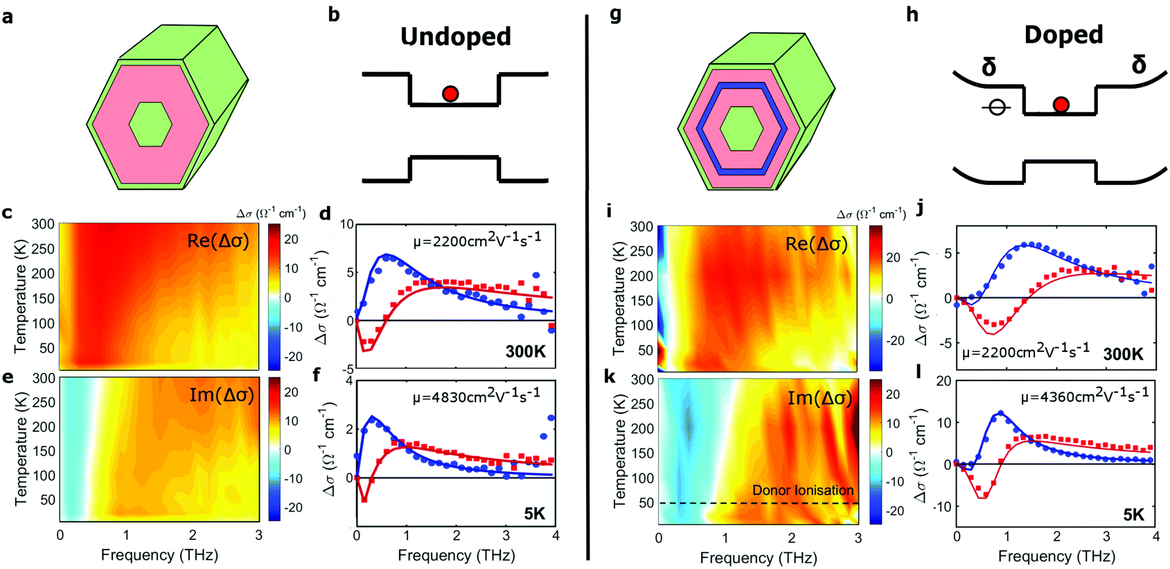 | ||
| Fig. 1 Schematic diagrams of the undoped (a) and modulation doped (g) core–shell GaAs/AlGaAs nanowires. Schematic diagrams of the bandstructure for the undoped (b) and modulation doped (h) GaAs/AlGaAs nanowires. Energy band diagrams calculated via a self-consistent solution of the Schrödinger and Poisson equations for both structures can be found in the ESI.† Colour maps of the real and imaginary components of the nanowire photoconductivity as a function of frequency and temperature for undoped (c), (e) and modulation doped (i), (k) nanowires. The dashed black line for the modulation doped nanowires represents the ionisation temperature of the Si dopants calculated from the photoconductivity lifetimes. Sample time-resolved photoconductivity spectra at room temperature and at the lowest temperature of 5 K for the undoped (d), (f) and modulation doped (j), (l) nanowires. | ||
The time resolved photoconductivity and carrier dynamics in the frequency domain were measured at a range of temperatures from 5 K to 300 K via the optical pump, terahertz probe (OPTP) setup described in the ESI.† The nanowires were photoexcited with a near-infrared laser of wavelength 800 nm (Ephoton = 1.55 eV) and pulse duration of 35 fs at fluences between 0.46 and 225 μJ cm−2. Excitation at this wavelength only allows electron–hole pairs to be selectively generated in the central core region and capping layer of the nanowire and not in the AlGaAs shell. The photoexcitation induces a change, ΔE, in the transmission of the electric field of the terahertz probe pulse through the nanowires, E. The value of ΔE/E is then proportional to the photoinduced nanowire conductivity and thereby the change in free carrier concentration45 (see ESI†). Thus, OPTP spectroscopy may be thought of as an electrical transport measurement technique with very high temporal resolution, since it probes conductivity dynamics. The terahertz conductivity signal is dominated by the charge species that have the highest product of carrier density and mobility (as is also the case in Hall measurements). As electrons in GaAs have approximately an order of magnitude higher mobility than heavy holes, the photoinduced conductivity is therefore assumed to arise predominantly from the photoexcited electrons for both samples. This photoinduced conductivity can then be measured as a function of time after photoexcitation and as a function of frequency to extract key parameters, such as doping densities, carrier mobilities and carrier lifetimes.45
3. Results and discussion
3.1. Effect of donor ionisation
Firstly, we examine donor ionisation and the effect of temperature on the electron mobility in both undoped and modulation doped nanowires. Photoconductivity spectra were measured for ensembles of nanowires at an excitation fluence of 225 μJ cm−2 for temperatures ranging from 5 K to 300 K. The real and imaginary parts of photoconductivity for undoped nanowires at a time 25 ps after photoexcitation are displayed in Fig. 1c and e respectively. The corresponding data for the modulation doped nanowires are shown in Fig. 1i and k. Two sets of photoconductivity spectra are extracted from each of these datasets for two temperatures, 5 K and 300 K, and are displayed for both undoped (Fig. 1d and f) and doped nanowires (Fig. 1j and l). Looking first at the data from the undoped nanowires (Fig. 1c–f), for all temperatures, a clear Lorentzian response in the photoconductivity is seen, with a resonance observed at terahertz frequencies. A significant narrowing of the resonance can be seen as the temperature is lowered (Fig. 1f), which is associated with increased electron mobility at low temperature. Likewise, for the modulation doped nanowires (Fig. 1j and l), a similar narrowing of the Lorentzian response can be observed as the temperature is lowered; however, the resonant frequency is shifted up in frequency compared with the undoped nanowires, especially at temperatures larger than 50 K.This Lorentzian resonance is associated with plasmons in the nanowires. The lower free charge-carrier densities in semiconductor nanowires, compared with their metallic counterparts,46 results in a resonant frequency within the terahertz range.47,48 The presence of such plasmon modes in GaAs nanowires and modulation doped GaAs/AlGaAs structures has already been demonstrated.42,49 In photoconductivity spectra, the resonant frequency lies at the maximum of the real component of the photoconductivity and where the imaginary component crosses zero. For the undoped nanowires (Fig. 1c and e), a slight redshift in the plasma frequency is observed. This is a result of fewer electrons being photoexcited at low temperatures, owing to a drop in the absorption coefficient for the 800 nm photons. For the modulation doped nanowires (Fig. 1i and k), a more distinct red-shift in the plasma frequency with decreasing temperature is observed. This red-shift coincides with decreasing free electron density and is a key attribute of plasmon modes. At low temperatures, the free electron concentration is reduced as an effect of freeze-out and thus there are fewer electrons to contribute to the plasmon mode, leading to a lower resonant frequency. From the colour maps of the photoconductivity spectra, this red-shift in resonant frequency can be seen most clearly in the imaginary component of the photoconductivity (Fig. 1e and k), where the white line depicts the plasma frequency. In contrast to the undoped nanowires, a clear transition in the position of the plasmon resonance can be seen at ∼50 K. As will be discussed later, this transition coincides with the ionisation temperature of the Si dopants. As the dopants are ionised, there is a marked increase in free carrier concentration, which leads to a sharp blue-shift in the resonant frequency, as depicted by the photoconductivity spectra in Fig. 1i and k.
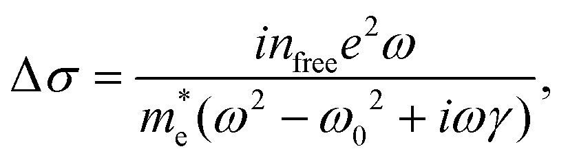
In Fig. 2a, we present the extrinsic electron density in the modulation doped nanowires as a function of temperature, which allows us to determine the Si donor ionisation energy. The extrinsic electron concentration in Fig. 2a can be extracted from the OPTP photoconductivity data in Fig. 1i and k, by noting that the complex photoconductivity of a free electron plasma with a plasmon resonance can be described by
 | (1) |
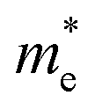 is the effective electron mass, γ is the momentum scattering rate and nfree is the free electron density. For undoped samples, the extrinsic electron density is negligible and nfree is therefore assumed to be equal to the photoexcited electron density nphoto. ω0 is the plasmon resonant frequency, which is given by:
 | (2) |
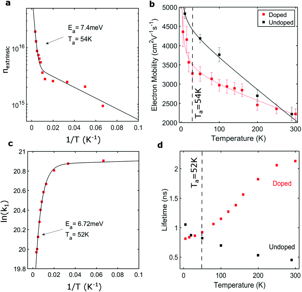 | ||
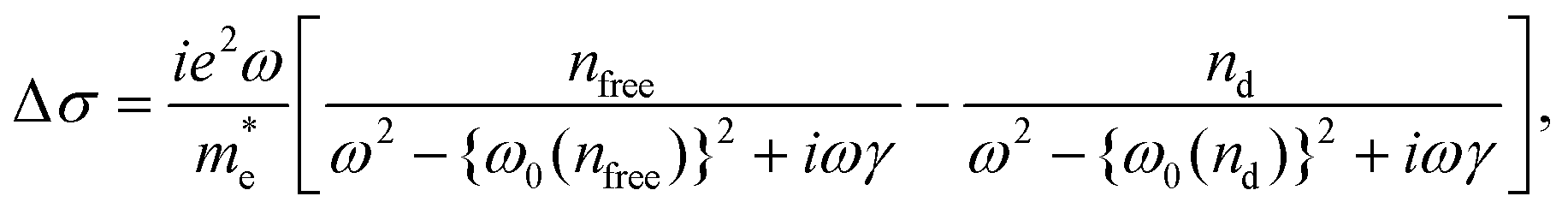
| Fig. 2 (a) The logarithm of the extrinsic electron concentration as a function of inverse temperature for the modulation doped core–shell GaAs/AlGaAs nanowires. (b) Electron mobilities as a function of temperature for the modulation doped (red) and undoped nanowires (black). Solid red and black lines show fits of a power temperature dependence for the electron mobilities. (c) The logarithm of the photoconductivity lifetimes as a function of inverse temperature for the modulation-doped core–shell GaAs/AlGaAs nanowires. (d) Photoconductivity lifetimes, extracted from the photoconductivity decay traces shown in Fig. 3, as a function of temperature for the modulation doped (red) and undoped nanowires (black). | ||
For doped samples, even in the dark, there is still a significant free electron carrier concentration from donated extrinsic electrons, which also leads to a Lorentzian response. Thus, the free carrier density can no longer be attributed purely to the photoexcited electrons and the expression for the complex photoconductivity becomes:
 | (3) |
By globally fitting this equation to photoconductivity spectral data recorded for a range of photoexcitation fluences and times after photoexcitation, key parameters, such as the extrinsic electron density, nd and scattering rate, γ, can be extracted. For each set of photoconductivity spectra recorded at a specific temperature, nd was set as a global parameter, while nphoto and γ were used as local fitting parameters for each spectrum. This is valid as, at a particular temperature, the photoexcited electron density and scattering rate change with photoexcitation fluence and time after photoexcitation, while the density of donated electrons should not change. For all fits, f was fixed to 0.25.28,49,50 Using this approach, the extrinsic electron concentration within the core of the modulation doped GaAs nanowires was found to be nd = 1.90 ± 0.8 × 1016 cm−3 at room temperature. The large difference between this measured value of nd and the Si ion concentration ND arises because ionised electrons are transferred from the small delta-doped region to the much larger volume of the GaAs core. This effect has been simulated via Schrödinger and Poisson simulations50 (as shown in Fig. S1 of the ESI†), showing remarkable agreement between the measured and simulated value for nd. The full temperature dependence of the donated electron density, nd was then extracted and plotted as function of inverse temperature, as shown in Fig. 2a.
We found the activation energy of Si donors in the modulation-doped nanowires to be 7.4 ± 0.57 meV using Arrhenius analysis, as depicted by the solid line in Fig. 2a. Significantly, the activation temperature, Ta = Ea/kb = 57 ± 7 K, matches the temperature, at which a transition in the resonant frequency is seen in the photoconductivity spectral colour map, shown in Fig. 1k, suggesting that this shift is a direct observation of donor ionisation. Below 100 K, an activation energy of 1.8 ± 0.14 meV (T = 19 ± 2 K) is also observed, suggesting the presence of other shallow donor impurities in the GaAs/AlGaAs structures. Such unintentional shallow impurities have also been observed in previous studies on high-quality GaAs/AlGaAs planar heterostructures.51
We confirm the values of the donor activation energies via an alternative method based on THz photoconductivity lifetimes. Fig. 2c shows an Arrhenius plot constructed from photoconductivity decay lifetimes measured from the modulation doped nanowires over the temperature range 5–300 K (THz photoconductivity decay curves are shown in Fig. 3). Via this method, we measured an activation energy of 6.72 ± 0.52 meV (52 ± 6 K), which not only coincides with the ionisation energy extracted from the extrinsic electron concentrations, but also with the theoretical value of 6 meV for Si donors in MBE-grown AlGaAs.52 These results also highlight THz spectroscopy as an accurate method for extracting activation energies of samples without the need to apply electrical contacts.
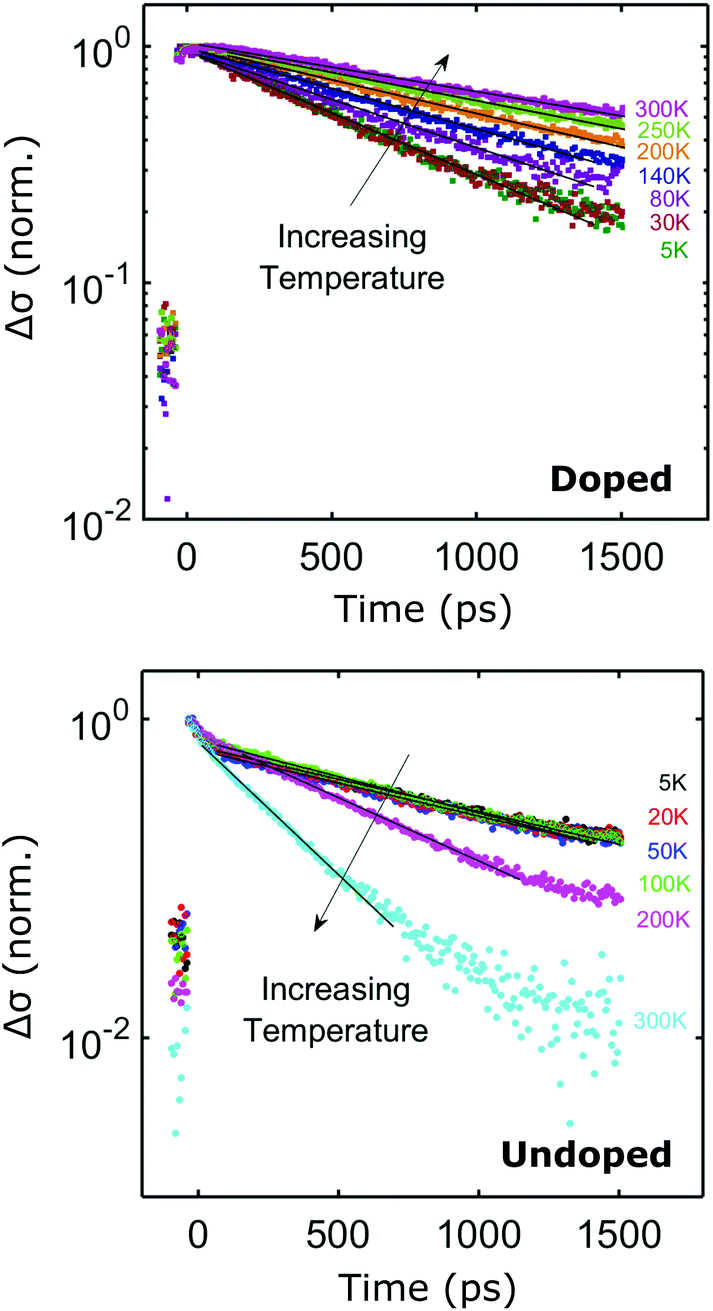 | ||
| Fig. 3 Normalised photoconductivity decay curves plotted as a function of time after photoexcitation at varying temperatures between 5 K and 300 K for (a) modulation doped and (b) undoped reference nanowires. Solid black lines depict monoexponential fits from which the carrier lifetimes are (shown in Fig. 2d) extracted. | ||
3.2. Temperature dependence of the electron mobility
A fundamental understanding of charge scattering mechanisims in nanowires will facilitate the development of higher mobility and higher speed NW devices. In order to understand the mechanisms that limit charge mobility in doped nanowires, we observed the dependence of THz photoconductivity spectra on temperature. By utilising the scattering rates taken from fits of the photoconductivity spectra shown in Fig. 1c,e,i and k, the electron mobility as a function of temperature was extracted and plotted in Fig. 2b. At 5 K, a high electron mobility of 4360 ± 380 cm2 V−1 s−1 was extracted for the modulation doped sample. This value is similar to the mobility of the undoped reference sample (4830 ± 140 cm2 V−1 s−1). For both samples, the carrier mobility decreased with increasing temperature, with a room temperature electron mobility of 2220 ± 130 cm2 V−1 s−1 for the doped nanowires and 2220 ± 180 cm2 V−1 s−1 for the undoped nanowires. At both the low and high temperature limits, the electron mobilities for the doped and undoped nanowires are comparable, yet the behaviour of the mobility at intermediate temperatures differ. For the undoped sample, no significant change in gradient is observed in the temperature-dependent electron mobilities, and the electron mobility follows the form μ ∼ T−0.64 for all temperatures between 5 K and 300 K. This temperature dependence for the electron mobilities is attributed to a combination of the dominant longitudinal optical (LO) phonon scattering and ionised impurity scattering due to background unintentional doping within the nanowires. For pure LO phonon scattering in a system, the electron mobility is theoretically predicted to be proportional to T−1/2.53 Yet, for bulk GaAs, which displays a combination of LO phonon scattering, ionised impurity and interface scattering, the mobility has been reported54 to vary according to T−1. The experimental exponent obtained here for the undoped nanowires therefore falls between values for pure LO phonon scattering and the exponent measured for bulk GaAs.54 For the modulation doped sample, a clear change in gradient for the mobilities can be seen at the donor ionisation temperature. Below 50 K, the electron mobility decreases rapidly with increasing temperature, with μ ∼ −T, as shown by the fit in Fig. 2b. This linear dependence of electron mobility with temperature has previously been observed in temperature-dependent mobility studies on planar modulation doped GaAs/AlGaAs heterostructures and can be attributed to a superposition of scattering mechanisms, which are all significant at low temperatures: acoustic-phonon (piezoelectric and deformation potential) scattering; remote background impurity scattering; interface, defect and alloy disorder scattering.55,56 Given the high surface area to volume ratio of the nanowire core, and the distance of Si dopants from the core, the effect of interface scattering is expected to be the dominant low temperature scattering mechanism. Interestingly, at temperatures above 50 K, the electron mobility follows the ideal form, μ ∼ T−1/2, for LO phonon scattering. Thus, our results are consistent with the electron mobility in modulation doped nanowires being primarily limited by LO phonons at room temperature.To further help separate the mechanisms responsible for electron scattering in modulation doped nanowires, we observe and model the temperature dependence of photoluminescence (PL) broadening. PL spectra were measured at temperatures between 5 K and 300 K from ensembles of modulation doped and undoped nanowires. NW samples were photoexcited with 100 fs laser pulses at a central wavelength of 740 nm with a fluence of 500 μJ cm−2. The PL spectra are shown in Fig. S5 and S6 of the ESI.†Fig. 4a shows full width at half maxima (FWHM) of the PL emission peak as a function of temperature. PL broadening arises from a range of mechanisms that show differing temperature dependencies. Specifically, the temperature dependence of the PL linewidth Γ(T) can be expressed as the sum,57,58
| Γ(T) = Γ0 + Γimp + ΓLO + Γac | (4) |
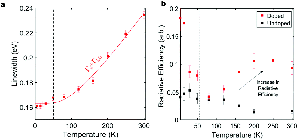 | ||
| Fig. 4 (a) Photoluminescence linewidths of modulation doped nanowires as a function of temperature. The solid line is a fit of section 3.2 to the data. (b) Radiative efficiencies as a function of temperature for both the undoped (black) and doped (red) nanowires. The dashed lines indicate the ionisation temperature extracted from the terahertz photoconductivity spectra in Fig. 1k. | ||
3.3. Temperature dependence of radiative efficiency and photoconductivity lifetime
Finally, we consider the radiative efficiency of undoped and modulation doped nanowires. Radiative efficiency is a key parameter for developing solar cells,62,63 lasers11 and LEDs64 based on nanowires. Fig. 4a and b shows the radiative efficiency of both undoped and modulation doped nanowires over a temperature range from 5 K and 300 K for an excitation fluence of 500 μJ cm−2. Full details of experimental setup and calculations for the radiative efficiency can be found in the ESI,† along with a detailed explanation of the low-temperature behaviour, where excitonic effects dominate. At room temperature, a radiative efficiency of 9.4 ± 1.2% is seen, an order of magnitude higher than for the undoped sample. We now compare the temperature dependence of the photoinjected electron lifetime in the nanowires (shown in Fig. 2d), with the temperature dependence of the radiative efficiency (Fig. 4c). Above 50 K, for modulation doped nanowires, both the radiative efficiency and photoinjected electron lifetimes increase with increasing temperature, whereas for the undoped nanowires the opposite relationship with temperature is observed. This is somewhat counterintuitive as one would expect an increase in radiative efficiency to lead to a reduction rather than an increase in electron lifetime, as the excited electrons recombine more efficiently. However, this simple analysis ignores changes in nonradiative recombination with temperature. Indeed, our results support the hypothesis that trapping of charge carriers in defects at the core–shell interface dominates the recombination dynamics in core–shell nanowires.28 The increase in radiative efficiency of the modulation doped nanowires can therefore be attributed to donated extrinsic electrons filling and hence passivating interfacial trap states, thereby reducing the non-radiative recombination rate. This would have the observed effect of boosting both the electron lifetime and the radiative efficiency. This is an exciting result, as it suggests that the increase in radiative efficiency at room temperature for the doped nanowires is a direct result of passivation of trap states, which may be achieved through well designed modulation doping. Recently, p-doping in GaAs nanowires has also been shown to increase radiative efficiency in unpassivated nanowires, allowing for nanowire lasing to be achieved at room temperature.11 Thus, modulation doped nanowires are promising candidates for use in optoelectronic devices, such as solar cells, nanolasers and LEDs, owing to their excellent radiative performance at both low and high temperatures.4. Conclusions
In conclusion, we have conducted the first temperature-dependent THz spectroscopy study of the charge carrier dynamics of GaAs/AlGaAs core–shell modulation doped nanowires. From both photoconductivity lifetime and spectral measurements, an activation energy of 6.7 ± 0.5 meV (T = 52 K) was extracted for the Si dopants, which coincides with the theoretical value for bulk AlGaAs. An increase in photoconductivity lifetime with increasing temperature was seen above the Si dopant ionisation temperature. This is a direct effect of the donor electrons passivating trap states at the core–shell interface, prolonging carrier lifetime. An increase in radiative efficiency above this ionisation temperature is also observed from PL spectra, as increased passivation of trap states allows for a reduction in non-radiative recombination and thereby increased radiative recombination. Furthermore, the electron mobility was extracted for temperatures from 5 K to 300 K. For the modulation doped nanowires, the electron mobility was also found to decrease with increasing temperature, with a transition between scattering mechanisms at the ionisation temperature. Below 50 K, the electron mobility was found to be dominated by interface scattering; whereas above 50 K, LO phonon scattering was determined to be the dominant scattering mechanism. A high electron mobility of 4360 ± 380 cm2 V−1 s−1 was found at 5 K, with a room temperature mobility of 2200 ± 130 cm2 V−1 s−1. These results indicate that electron mobilities and radiative efficiency of high quality doped nanowires may be further increased by improved interface engineering combined with modulation doping schemes that reduce the effectiveness of both impurity and interface scattering.Acknowledgements
The authors thank the EPSRC (UK) for financial support. The Swiss National Science Foundation via projects nr137648 and 156081, the NCCR-QSIT and the NanoTera program though the Synergy project are greatly acknowledged.References
- W. Lu and C. M. Lieber, J. Phys. D: Appl. Phys., 2006, 39, R387–R406 CrossRef CAS.
- J. a. Czaban, D. a. Thompson and R. R. LaPierre, Nano Lett., 2009, 9, 148–154 CrossRef CAS PubMed.
- M. Law, L. E. Greene, J. C. Johnson, R. Saykally and P. Yang, Nat. Mater., 2005, 4, 455–459 CrossRef CAS PubMed.
- Y. Dong, B. Tian, T. Kempa and C. M. Lieber, Nano Lett., 2009, 9, 2183–2187 CrossRef CAS PubMed.
- P. Krogstrup, H. I. Jørgensen, M. Heiss, J. V. Holm, M. Aagesen, J. Nygard and A. Fontcuberta, Nat. Photonics, 2013, 7, 306–310 CrossRef CAS.
- S. Dayeh, D. P. Aplin, X. Zhou, P. K. Yu, E. Yu and D. Wang, Small, 2007, 3, 326–332 CrossRef CAS PubMed.
- K. Tomioka, M. Yoshimura and T. Fukui, Nature, 2012, 488, 189–192 CrossRef CAS PubMed.
- S. Morkötter, N. Jeon, D. Rudolph, B. Loitsch, D. Spirkoska, E. Hoffmann, M. Döblinger, S. Matich, J. Finley, L. Lauhon, G. Abstreiter and G. Koblmüller, Nano Lett., 2015, 15, 3295–3302 CrossRef PubMed.
- S. Gradečak, F. Qian, Y. Li, H.-G. Park and C. M. Lieber, Appl. Phys. Lett., 2005, 87, 173111 CrossRef.
- D. Saxena, S. Mokkapati, P. Parkinson, N. Jiang, Q. Gao, H. H. Tan and C. Jagadish, Nat. Photonics, 2013, 7, 963–968 CrossRef CAS.
- T. Burgess, D. Saxena, S. Mokkapati, Z. Li, C. R. Hall, J. A. Davis, Y. Wang, L. M. Smith, L. Fu, P. Caroff, H. H. Tan and C. Jagadish, Nat. Commun., 2016, 7, 11927 CrossRef CAS PubMed.
- E. D. Minot, F. Kelkensberg, M. Van Kouwen, J. a. Van Dam, L. P. Kouwenhoven, V. Zwiller, M. T. Borgström, O. Wunnicke, M. A. Verheijen and E. P. A. M. Bakkers, Nano Lett., 2007, 7, 367–371 CrossRef CAS PubMed.
- K. Tomioka, J. Motohisa, S. Hara, K. Hiruma and T. Fukui, Nano Lett., 2010, 10, 1639–1644 CrossRef CAS PubMed.
- M. Tchernycheva, P. Lavenus, H. Zhang, A. Babichev, G. Jacopin, M. Shahmohammadi, F. H. Julien, R. Ciechonski, B. Vescovi and O. Kryliouk, Nano Lett., 2014, 14, 2456–2465 CrossRef CAS PubMed.
- M. S. Vitiello, D. Coquillat, L. Viti, D. Ercolani, F. Teppe, A. Pitanti, F. Beltram, L. Sorba, W. Knap and A. Tredicucci, Nano Lett., 2012, 12, 96–101 CrossRef CAS PubMed.
- K. Peng, P. Parkinson, L. Fu, Q. Gao, N. Jiang, Y.-N. Guo, F. Wang, H. J. Joyce, J. L. Boland, H. H. Tan, C. Jagadish and M. B. Johnston, Nano Lett., 2015, 15, 206–210 CrossRef CAS PubMed.
- K. Peng, P. Parkinson, J. L. Boland, Q. Gao, Y. C. Wenas, C. L. Davies, Z. Li, L. Fu, M. B. Johnston and H. H. Tan, Nano Lett., 2016, 16, 4925–4931 CrossRef CAS PubMed.
- L. Romeo, D. Coquillat, E. Husanu, D. Ercolani, A. Tredicucci, F. Beltram, L. Sorba, W. Knap and M. S. Vitiello, Appl. Phys. Lett., 2014, 105, 231112 CrossRef.
- Y. Cui, X. Duan, J. Hu and C. M. Lieber, J. Phys. Chem. B, 2000, 104, 4–7 Search PubMed.
- K. Haraguchi, T. Katsuyama, K. Hiruma and K. Ogawa, Appl. Phys. Lett., 1992, 60, 745–748 CrossRef CAS.
- C. Gutsche, A. Lysov, I. Regolin, K. Blekker, W. Prost and F.-j. Tegude, Nanoscale Res. Lett., 2010, 6, 65 Search PubMed.
- C. Gutsche, I. Regolin, K. Blekker, A. Lysov, W. Prost and F. J. Tegude, J. Appl. Phys., 2009, 105, 024305 CrossRef.
- O. Salehzadeh, X. Zhang, B. D. Gates, K. L. Kavanagh and S. P. Watkins, J. Appl. Phys., 2012, 112, 94323 CrossRef.
- S. Suomalainen, T. V. Hakkarainen, T. Salminen, R. Koskinen, M. Honkanen, E. Luna and M. Guina, Appl. Phys. Lett., 2015, 107, 012101 CrossRef.
- J. Wallentin and M. T. Borgström, J. Mater. Res., 2011, 26, 2142–2156 CrossRef CAS.
- E. Dimakis, M. Ramsteiner, A. Tahraoui, H. Riechert and L. Geelhaar, Nano Res., 2012, 5, 796–804 CrossRef CAS.
- K. Sladek, V. Klinger, J. Wensorra, M. Akabori, H. Hardtdegen and D. Grützmacher, J. Cryst. Growth, 2010, 312, 635–640 CrossRef CAS.
- J. L. Boland, A. Casadei, F. Matteini, C. L. Davies, F. Jabeen, H. J. Joyce, L. M. Herz, A. Fontcuberta and M. B. Johnston, ACS Nano, 2016, 10, 4219–4227 CrossRef CAS PubMed.
- M. Hilse, M. Ramsteiner, S. Breuer, L. Geelhaar and H. Riechert, Appl. Phys. Lett., 2010, 96, 193104 CrossRef.
- A. Casadei, P. Krogstrup, M. Heiss, J. a. Röhr, C. Colombo, T. Ruelle, S. Upadhyay, C. B. Sørensen, J. Nygård and A. Fontcuberta I Morral, Appl. Phys. Lett., 2013, 102, 013117 CrossRef.
- J. Dufouleur, C. Colombo, T. Garma, B. Ketterer, E. Uccelli, M. Nicotra and A. Fontcuberta I Morral, Nano Lett., 2010, 10, 1734–1740 CrossRef CAS PubMed.
- B. Ketterer, E. Mikheev, E. Uccelli and A. Fontcuberta I Morral, Appl. Phys. Lett., 2010, 97, 2008–2011 CrossRef.
- L. Xu, Y. Su, Y. Chen, H. Xiao, L. A. Zhu, Q. Zhou and S. Li, J. Phys. Chem. B, 2006, 110, 6637–6642 CrossRef CAS PubMed.
- R. E. Algra, M. A. Verheijen, M. T. Borgström, L. Feiner, G. Immink, W. J. P. van Enckevort, E. Vlieg and E. P. A. M. Bakkers, Nature, 2008, 456, 369–372 CrossRef CAS PubMed.
- B. Ketterer, E. Uccelli and A. Fontcuberta i Morral, Nanoscale, 2012, 4, 1789–1793 RSC.
- C. S. Ponseca, H. Němec, J. Wallentin, N. Anttu, J. P. Beech, A. Iqbal, M. Borgström, M. E. Pistol, L. Samuelson and A. Yartsev, Phys. Rev. B: Condens. Matter Mater. Phys., 2014, 90, 1–7 CrossRef.
- L. Pfeiffer, K. W. West, H. L. Stormer and K. W. Baldwin, Appl. Phys. Lett., 1989, 55, 1888–1890 CrossRef CAS.
- H. Stormer, A. C. Gossard, W. Wiegmann and K. Baldwin, Appl. Phys. Lett., 1981, 39, 912–913 CrossRef.
- J. Jadczak, P. Plochocka, A. Mitioglu, I. Breslavetz, M. Royo and A. Bertoni, Nano Lett., 2014, 14, 1–21 CrossRef PubMed.
- D. Spirkoska, A. Fontcuberta i Morral, J. Dufouleur, Q. Xie and G. Abstreiter, Phys. Status Solidi RRL, 2011, 5, 353–355 CrossRef CAS.
- Z. Cui, R. Perumal, T. Ishikura, K. Konishi, K. Yoh and J. Motohisa, Appl. Phys. Express, 2014, 7, 85001 CrossRef.
- J. L. Boland, S. Conesa-Boj, G. Tütüncouglu, F. Matteini, D. Rüffer, A. Casadei, F. Gaveen, F. Amaduzzi, P. Parkinson, C. Davies, H. J. Joyce, L. M. Herz, A. F. Morral and M. B. Johnston, 40th International Conference on Infrared, Millimeter, and Terahertz waves (IRMMW-THz), 2015.
- K. Storm, F. Halvardsson, M. Heurlin, D. Lindgren, A. Gustafsson, P. M. Wu, B. Monemar and L. Samuelson, Nat. Nanotechnol., 2012, 7, 718–722 CrossRef CAS PubMed.
- S. Birner, T. Zibold, T. Andlauer, T. Kubis, M. Sabathil, A. Trellakis and P. Vogl, IEEE Trans. Electron Devices, 2007, 54, 2137–2142 CrossRef CAS.
- H. J. Joyce, J. L. Boland, C. L. Davies, S. Baig and M. B. Johnston, Semicond. Sci. Technol., 2016, 31, 1–21 CrossRef.
- W. L. Barnes, J. Opt. A: Pure Appl. Opt., 2006, 8, S87–S93 CrossRef.
- T. H. Isaac, W. L. Barnes and E. Hendry, Appl. Phys. Lett., 2008, 93, 241115 CrossRef.
- P. Kužel and H. Němec, J. Phys. D: Appl. Phys., 2014, 47, 374005 CrossRef.
- P. Parkinson, H. J. Joyce, Q. Gao, H. H. Tan, X. Zhang, J. Zou, C. Jagadish, L. M. Herz and M. B. Johnston, Nano Lett., 2009, 9, 3349–3353 CrossRef CAS PubMed.
- J. L. Boland, S. Conesa-Boj, P. Parkinson, G. Tütüncüoglu, F. Matteini, D. Rüffer, A. Casadei, F. Amaduzzi, F. Jabeen, C. L. Davies, H. J. Joyce, L. M. Herz, A. Fontcuberta i Morral and M. B. Johnston, Nano Lett., 2015, 15, 1336–1342 CrossRef CAS PubMed.
- E. Shubert and K. Ploog, Phys. Rev. B: Condens. Matter, 1984, 30, 7021–7029 CrossRef.
- M. Watanabe and H. Maeda, Jpn. J. Appl. Phys., 1984, 23, L734–L736 CrossRef.
- P. Yu and M. Cardona, Fundamentals of Semiconductors, Springer, 2010, ch. 5 Search PubMed.
- I. Akasaki and T. Hara, J. Phys. Soc. Jpn., 1965, 20, 2292 CrossRef CAS.
- W. Walukiewicz, H. Ruda, J. Lagowski and H. Gatos, Phys. Rev. B: Condens. Matter, 1984, 30, 4571–4582 CrossRef CAS.
- S. Adachi, GaAs and Related Materials: Bulk Semiconducting and Superlattice Properties, World Scientific, 1994, p. ch. 15 Search PubMed.
- A. D. Wright, C. Verdi, R. L. Milot, G. E. Eperon, M. A. Pérez-Osorio, H. J. Snaith, F. Giustino, M. B. Johnston and L. M. Herz, Nat. Commun., 2016, 7, 11755 Search PubMed.
- O. Celik, E. Tiras, S. Ardali, S. B. Lisesivdin and E. Ozbay, Cent. Eur. J. Phys., 2011, 10, 485–491 Search PubMed.
- W. Peng, F. Jabeen, B. Jusserand, J. C. Harmand and M. Bernard, Appl. Phys. Lett., 2012, 100, 073102 CrossRef.
- P. A. Khomyakov, S. Karg, D. L. Dheeraj, B. Gotsmann, H. Weman, H. Riel, G. Signorello and E. Lo, Nat. Commun., 2014, 5, 3655 Search PubMed.
- P. Kusch, S. Breuer, M. Ramsteiner, L. Geelhaar, H. Riechert and S. Reich, Phys. Rev. B: Condens. Matter Mater. Phys., 2012, 86, 075317 CrossRef.
- O. D. Miller, E. Yablonovitch and S. R. Kurtz, Photovoltaics, IEEE J., 2012, 2, 1–27 CrossRef.
- Y. Cui, D. van Dam, S. A. Mann, N. J. J. van Hoof, P. J. van Veldhoven, E. C. Garnett, E. P. A. M. Bakkers and J. E. M. Haverkort, Nano Lett., 2016, 16, 6467–6471 CrossRef CAS PubMed.
- F. Qian, S. Gradečak, Y. Li, C. Y. Wen and C. M. Lieber, Nano Lett., 2005, 5, 2287–2291 CrossRef CAS PubMed.
Footnote |
| † Electronic supplementary information (ESI) available: Experimental details; Schrödinger–Poisson modelling; detailed description of data processing; full photoluminescence and terahertz photoconductivity datasets. See DOI: 10.1039/C7NR00680B |
| This journal is © The Royal Society of Chemistry 2017 |