
 Open Access Article
 This Open Access Article is licensed under a
 Creative Commons Attribution 3.0 Unported Licence
The passivating effect of cadmium in PbS/CdS colloidal quantum dots probed by nm-scale depth profiling†
Pip C. J.
Clark
 *a,
Hanna
Radtke
a,
Atip
Pengpad
a,
Andrew I.
Williamson
a,
Ben F.
Spencer‡
a,
Samantha J. O.
Hardman§
a,
Marina A.
Leontiadou
a,
Darren C. J.
Neo¶
b,
Simon M.
Fairclough||
b,
Andrew A. R.
Watt
b,
Igor
Pis
cd,
Silvia
Nappini
c,
Federica
Bondino
c,
Elena
Magnano
ce,
Karsten
Handrup
f,
Karina
Schulte
f,
Mathieu G.
Silly
g,
Fausto
Sirotti
g and
Wendy R.
Flavell
a
*a,
Hanna
Radtke
a,
Atip
Pengpad
a,
Andrew I.
Williamson
a,
Ben F.
Spencer‡
a,
Samantha J. O.
Hardman§
a,
Marina A.
Leontiadou
a,
Darren C. J.
Neo¶
b,
Simon M.
Fairclough||
b,
Andrew A. R.
Watt
b,
Igor
Pis
cd,
Silvia
Nappini
c,
Federica
Bondino
c,
Elena
Magnano
ce,
Karsten
Handrup
f,
Karina
Schulte
f,
Mathieu G.
Silly
g,
Fausto
Sirotti
g and
Wendy R.
Flavell
a
aSchool of Physics and Astronomy and the Photon Science Institute, The University of Manchester, Manchester M13 9PL, UK. E-mail: pip.clark@manchester.ac.uk
bDepartment of Materials, University of Oxford, 16 Parks Road, Oxford OX1 3PH, UK
cLaboratorio TASC, IOM CNR, S.S. 14 km 163.5, 34149 Basovizza, Trieste, Italy
dElettra-Sincrotrone Trieste S.C.p.A., S. S. 14 Km 163.5, 34149 Basovizza, Trieste, Italy
eDepartment of Physics, University of Johannesburg, PO Box 524, Auckland Park 2006, South Africa
fMAX IV Laboratory, Lund University, Box 118, 221 00 Lund, Sweden
gSynchrotron SOLEIL, BP 48, Saint-Aubin, F91192 Gif sur Yvette CEDEX, France
First published on 10th April 2017
Abstract
Achieving control of the surface chemistry of colloidal quantum dots (CQDs) is essential to fully exploit their properties in solar cells, but direct measurement of the chemistry and electronic structure in the outermost atomic layers is challenging. Here we probe the surface oxidation and passivation of cation-exchanged PbS/CdS core/shell CQDs with sub nm-scale precision using synchrotron-radiation-excited depth-profiling photoemission. We investigate the surface composition of the topmost 1–2.5 nm of the CQDs as a function of depth, for CQDs of varying CdS shell thickness, and examine how the surface changes after prolonged air exposure. We demonstrate that the Cd is localized at the surface of the CQDs. The surface-localized products of oxidation are identified, and the extent of oxidation quantified. We show that oxidised sulfur species are progressively eliminated as Cd replaces Pb at the surface. A sub-monolayer surface ‘decoration’ of Cd is found to be effective in passivating the CQDs. We show that the measured energy-level alignments at PbS/CdS colloidal quantum dot surfaces differ from those expected on the basis of bulk band offsets, and are strongly affected by the oxidation products. We develop a model for the passivating action of Cd. The optimum shell thickness (of around 0.1 nm, previously found to give maximised power conversion efficiency in PbS/CdS solar cells) is found to correspond to a trade-off between the rate of oxidation and the introduction of a surface barrier to charge transport.
1. Introduction
Colloidal quantum dots (CQDs) are promising candidates as light absorbing components in photovoltaic technologies. Lead sulphide (PbS) CQDs have been heavily investigated and their use has resulted in near-record CQD solar cell efficiency.1 They cover an optimal bandgap range for both single and multi-junction solar cells as the bandgap energy can be tuned from the infrared to the ultraviolet region.2 Multiple exciton generation, a route to overcoming the Shockley–Queisser efficiency limit,3 has also been observed in PbS CQDs.4–8 The need for reduction in the cost of solar technology can also be accommodated by CQDs as they offer low-cost device processing.9However, PbS and other chalcogenide CQDs are inherently unstable when exposed to air. The oxidation which can occur changes the intrinsic properties by increasing the bandgap energy (reducing the absorption of visible light),4,10,11 and greatly reduces carrier lifetimes through non-radiative recombination due to the formation of trap states.12 This puts a limit on the working lifetime of a CQD-based solar device.13 Advances in creating air-stable PbS CQDs have been made through using halide ion treatments,13–16 and through the addition of an outer chalcogenide shell, as in PbS/CdS core/shell CQDs.17–21 With the addition of a nominally sub-monolayer CdS shell via cation exchange, Neo et al. have improved the power conversion efficiency of a simple heterojunction solar cell from 3.6% to 5.6%.17 This increase in efficiency was attributed to an increase in the open circuit voltage, caused by a reduction in recombination, a result of the introduced shell.22 A sub-monolayer CdS shell with an effective thickness of 0.1 nm (inferred from optical difference measurement) gave the optimum results, as thicker shells reduced the short circuit current.
The observation of substantially improved performance through incorporation of a sub-monolayer amount of notional ‘shell’ material raises important questions about the way in which Cd is incorporated into the CQDs, the true shell thickness and how this influences surface passivation and electronic structure. Indeed in general, our knowledge of CQD surfaces at the atomic scale remains limited, much of it inferred from bulk properties, and rather little of it directly measured. To answer such questions, it is necessary to characterize the depth-dependent composition of CQDs, and to be able to identify those species present only at the QD surface with sub-nm-scale precision.
Synchrotron-radiation (SR)-excited depth-profiling X-ray photoelectron spectroscopy (XPS) is one of very few techniques that can provide this information, because it allows for the photoelectron inelastic mean free path (IMFP) to be varied over distances commensurate with the nanoparticle size. By changing the photon energy, the kinetic energy (KE) of photoelectrons emitted from an elemental orbital of set binding energy (BE) changes.23 The IMFP is dependent on the photoelectron KE. By selecting appropriate photon energies, photoelectron spectra are measured from different elements in the CQDs in sets of constant sampling depth, offering significant advantages over conventional XPS. The technique has been used by ourselves and others to determine the shell structure of CQDs and nanoparticles,24–32 and to give insights into the mechanism of atmospheric oxidation.4,33,34 Further advantages of a SR source accrue in valence band photoemission, as the photon energy may be tuned to maximise the photoionisation cross section of the valence band states, improving the accuracy with which weak features such as the valence band maximum (VBM) may be located.
Here we use SR-excited depth profiling XPS to confirm the incorporation of Cd in the surface layers of PbS/CdS core/shell CQDs, where the Cd shell is grown by cation exchange. We combine these data with absorption and transmission electron microscopy (TEM) measurements, to determine the effective shell thickness of CdS, using methods developed by Shard et al.28,35 By identifying the different chemical species present at the surface34,36 we compare the extent of surface oxidation for different CdS shell thicknesses, and observe how the PbS/CdS CQD surface changes as a function of time in air. We show that early oxidation is progressively eliminated as Cd replaces Pb at the surface. We correlate this information with simultaneous photoemission measurements of the electronic structure near the VBM. We demonstrate that the surface electronic structure of the CQDs differs from that expected on the basis of bulk band alignments, resulting in a significant barrier to charge transport when a thick CdS shell is grown. We present a model for the passivating action of sub-monolayer Cd in these CQDs.
2. Experimental
2.1 PbS/CdS core/shell CQD synthesis
PbS CQD cores were synthesized by a procedure adapted from Hines and Scholes.37 The CdS shells were grown by cation exchange, in the procedure developed by Neo et al.38 The details of this synthesis have been described previously.172.2 Post-synthesis ligand exchange
After synthesis the original oleic acid or oleylamine ligands were exchanged for either butylamine or 3-mercaptopropionic acid (3-MPA). This was done to avoid sample charging when measuring photoemission,39 as the new ligands are shorter in length. The ligand exchange to butylamine and 3-MPA followed modified methods from Fairclough et al. and Zhang et al. respectively.39,40 The methods are outlined in the ESI.†2.3 Characterization
Optical absorption spectroscopy of the CQDs was measured using a Cary Varian 4000 UV-vis-NIR spectrophotometer with diluted CQD solution in a quartz cuvette.TEM was performed using a JEOL 2010 transmission electron microscope, operating at 200 kV, and the Oxford JEOL 2200MCO aberration-corrected, monochromated FED-TEM operating at 80 kV. The mean size of the CQDs was determined by fitting a Gaussian distribution curve to the experimental size histogram. The samples were prepared by dipping TEM grids into a dilute solution of CQDs and drying them in ambient conditions.
XPS was performed using beamlines at three synchrotron sources: the BACH beamline (35 < hν < 1600 eV, equipped with a Scienta R3000 hemispherical analyzer) at the Elettra synchrotron in Trieste, Italy; the TEMPO beamline, (50 < hν < 1500 eV, equipped with a SCIENTA SES 2002 electron energy analyzer) at Synchrotron SOLEIL, France; and I311 (43 < hν < 1500 eV, equipped with a SCIENTA SES200 hemispherical analyzer) at MAX-lab in Lund, Sweden. XP spectra were recorded at room temperature in normal emission geometry, using light linearly polarized in the horizontal plane. The total instrumental resolution ranged from 170 meV (at 250 eV photon energy) to 1.26 eV (at 1400 eV photon energy). Data were collected in sets of spectra at the same photoelectron KE, between 135 eV and 1000 eV KE. As the IMFP of photoelectrons emitted from the sample is dependent on their KE, the depth probed increases with KE.23 XPS spectra were corrected for photon flux and then fitted using CasaXPS.41 The areas of XPS peaks were corrected for photoionization cross section and asymmetry factors.42 The S 2p spectra were calibrated to a bulk PbS S 2p3/2 component at 160.7 eV,43,44 and the other spectra were then calibrated using this reference point. The resulting BEs were consistent with available literature values. More detail is given in the ESI.†
For XPS analysis CQD samples were drop cast onto an indium tin oxide (ITO) substrate and entered the fast entry lock of the ultra-high vacuum chamber within 5 to 30 minutes of deposition. A separate series of samples was deposited in the same way and aged in air for controlled periods of up to eight months before examination.
3. Results
3.1 Optical absorption and TEM
A notable feature of PbS/CdS CQDs prepared by the cation-exchange procedure of Neo et al. is that the core/shell CQDs preserve the approximate initial diameter of the PbS CQDs (as measured by TEM), whereas the PbS core decreases in size during shell formation (as measured by its optical absorption).17 This appears to be true over a wide range of CQD sizes. As examples, Fig. 1 shows the absorbance curves of two PbS/CdS samples of significantly different size, before and after cation exchange. The 1S excitonic absorption peak was used to find the band gap of the quantum dots before and after cation exchange. From this the core diameter was estimated using the empirical relationship proposed by Moreels et al.45 The reduction in core size after cation exchange, seen as a blue shift in the absorbance, was used to estimate the effective thickness of the Cd shell. This method has been established previously to characterize PbS/CdS CQDs of different shell thicknesses.17 In both samples shown in Fig. 1 the shell thickness was found to be approximately 0.1 nm. This is less than a monolayer thickness,46 and implies that a conformal CdS shell is not formed. We expect that this shell thickness carries a high error, as it is estimated from a small difference between fitted absorption energies. The investigation of the true shell structure, and calculation of a more accurate shell thickness is one aim of this paper.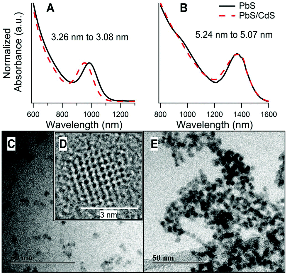 | ||
| Fig. 1 (A, B) Normalized absorbance curves of two PbS CQD samples before and after cation exchange to produce PbS/CdS core/shell CQDs. The blue shift occurs after cation exchange as the PbS core diameter decreases. The start and end PbS core diameters (estimated using an empirical relationship)45 are indicated on the figure. (C, E) TEM images of PbS/CdS core/shell CQDs. (D) is a high resolution image of one PbS/CdS CQD. (A), (C) and (D) are taken from a 3.1 ± 0.2 nm diameter CQD. (B) and (E) are from a 5.2 ± 0.2 nm diameter CQD. | ||
TEM images of these two quantum dot samples are presented in Fig. 1C–E. The overall average diameters of the two core/shell QD samples shown were determined from the TEM images as 3.1 ± 0.2 nm and 5.2 ± 0.2 nm. Here, we compile data from a range of samples of both sizes, in order to extract the underlying common trends. For simplicity, these are referred to as ‘3 nm’ and ‘5 nm’ samples.
3.2 Surface composition
SR-excited depth profiling XPS was used to study the composition of the CQDs. We begin by addressing the depth distribution of Cd and organic ligands.Fig. 2A and B show the ratio of Cd to Pb and the ratio of bound ligands to Pb respectively, as determined from XPS of the Cd 3d, Pb 4d, S 2p and N 1s core level signals, at different sampling depths for five different PbS/CdS samples. Fig. 2C shows the intensity of the XPS signal against the depth that the photoelectrons originated from, for a 3 nm diameter PbS CQD. This highlights the surface sensitivity of XPS, as the intensity decays exponentially with depth. The sampling depths at each kinetic energy are also shown in Fig. 2C. Calculation of the sampling depths is discussed in section 3.3.
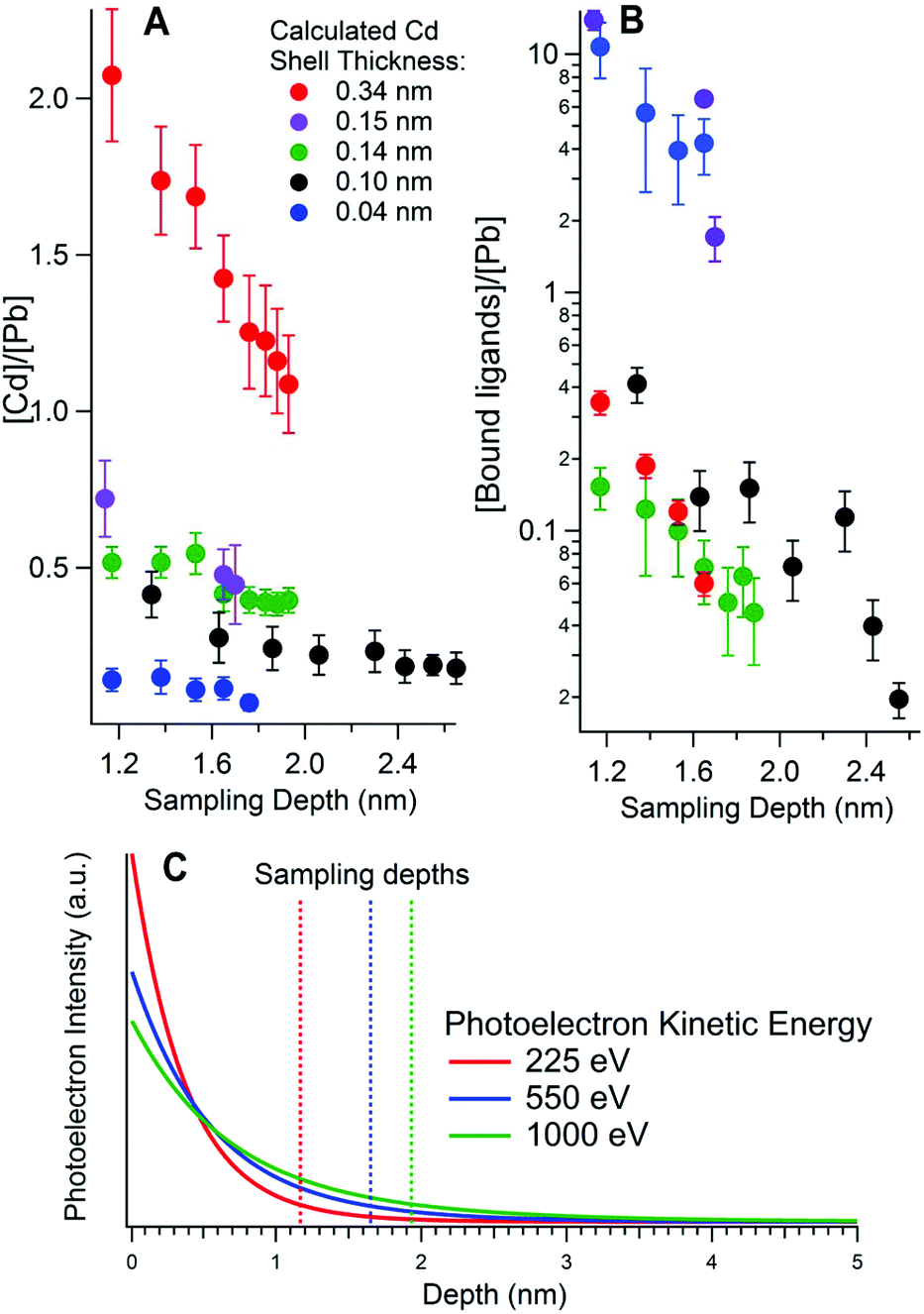 | ||
| Fig. 2 Elemental ratios as a function of calculated sampling depth for (A) Cd to Pb, and (B) ligands to Pb as calculated from synchrotron-excited X-ray Photoelectron Spectroscopy. Each sample is labelled with its effective shell thickness, calculated from these ratios. The black markers correspond to a quantum dot core diameter of 5 nm, while the remaining samples have a core diameter of 3 nm. (C) The photoelectron intensity variation with depth for photoelectrons emitted from a 3 nm PbS CQD for photoelectrons of three different kinetic energies. The sampling depth, where 95% of the signal originates from (see ESI†), is shown with a dashed line. The ligands were butylamine except for the 0.15 nm shell sample, where 3-mercaptopropionic acid (3-MPA) was used. The ligand-to-Pb ratio is calculated using N or S in the ligands (for butylamine and 3-MPA respectively). For the 0.34 nm shell sample in (B) the N 1s peak could not be fitted adequately for sampling depths greater than 1.7 nm, as it was small enough to be comparable with the noise. | ||
For each sample the overall trend is that the amount of Cd relative to Pb decreases as the sampling depth increases, as more of the Pb cores are probed. This provides compelling evidence that Cd is incorporated only at the surfaces of the PbS quantum dots. Accordingly, the samples featured in Fig. 2 are labelled by their effective CdS shell thicknesses, calculated from the Cd-to-Pb ratios measured in XPS as detailed in section 3.3.
We have also studied the effect of washing CQDs after ligand exchange to remove excess unbound ligands. Good washing is important as an excess of insulating organic ligands can be detrimental to CQD solar cell efficiency.47–50 For this study the ligand-to-Pb ratio was calculated from XPS (Fig. 2B, displayed using a log scale). There is a decrease in the ligand-to-Pb ratios with sampling depth but with a significantly steeper gradient than found for the Cd-to-Pb ratios. This increased depth dependence points to the ligands being situated on the very surface of the quantum dot, as we would anticipate. For the 0.15 nm and 0.04 nm Cd shell samples the ligand-to-Pb ratio is much higher than in the other samples. This indicates less successful washing of the quantum dots after ligand exchange, where excess ligands are normally removed. Indeed, in both these cases the ligands were found in XPS in both bound and unbound chemical states as shown in Fig. S4 in the ESI.†
3.3 Calculating the shell thickness
Two related models for calculating the shell thickness of a core–shell quantum dot were used. Both are analytical models developed by Shard et al., for use with XPS data.28,35 Both methods are appropriate to randomly ordered spherical nanoparticles where the effects of directional elastic scattering can be neglected.51 We used one method to calculate the variation in the number ratio of shell and core elements with sampling depth for a fixed core diameter (determined by absorbance measurements, Fig. 1) and variable shell thickness. The predicted variation was compared to the ratios extracted from depth profiling XPS data, as shown in Fig. 3. In the second method, the core diameter, the Cd![[thin space (1/6-em)]](https://www.rsc.org/images/entities/char_2009.gif) :Pb ratio, and other parameters for each sampling depth were used to calculate a shell thickness for every sampling depth, which were then averaged. Good agreement was found between the two methods.
:Pb ratio, and other parameters for each sampling depth were used to calculate a shell thickness for every sampling depth, which were then averaged. Good agreement was found between the two methods.
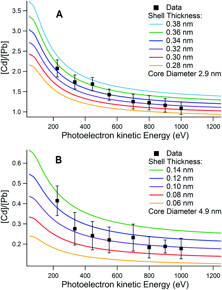 | ||
| Fig. 3 Plots showing [Cd]/[Pb] ratios measured with XPS at different photoelectron kinetic energies, compared with the variation calculated using the core–shell model of Shard et al.28 for a series of different CdS shell thicknesses on (A) a 2.9 nm diameter core and (B) a 4.9 nm core. Core diameters were obtained from optical absorption measurements using the empirical relationship proposed by Moreels et al.45 The sample in (A) was found to have an effective shell thickness of 0.34 ± 0.04 nm, and in (B) 0.10 ± 0.02 nm. | ||
The sampling depth is defined as the depth from which 95% of the detected electrons originate. For a planar surface the sampling depth is approximately 3λ, where λ is the photoelectron IMFP. For a spherical particle, with radii of the order of a photoelectron IMFP, the curvature of the particle needs to be accounted for.28 The XPS sampling depth in a CQD is then lower than 3λ, and is dependent on the size of the CQD. Values of λ at different photoelectron kinetic energies were calculated with the TPP-2M formula.52–54 More details are presented in the ESI.†
Examples of the results of shell thickness calculations are shown in Fig. 3 and in the ESI, Fig. S2.† The XPS-calculated shell thicknesses are compared with those obtained from optical absorption in the ESI.† For the sample shown in Fig. 3A the shell thickness was determined to be 0.34 ± 0.04 nm, and for the sample shown in Fig. 3B, 0.10 ± 0.02 nm. In the case of the thicker (0.34 nm) shell there was significant difference between the diameter of the CQD found by TEM (Fig. 1D 3.1 ± 0.2 nm) and the overall core–shell QD diameter found from the XPS-calculated shell thickness combined with the core size determined from optical absorption measurements (3.8 ± 0.1 nm). This may suggest that some alloying occurred between the core and shell during synthesis, and is discussed in more detail in section 4.1.
3.4 The effect of aging on surface composition
To investigate the aging process of PbS/CdS quantum dots, CQDs were examined by SR-excited XPS after exposure to air for periods of up to eight months. The atmospheric aging of PbS nanoparticles has been examined in this way by ourselves4,33 and others.13 Long-term exposure to air is known to result in the formation of sulphite and sulphate species that are highly localized at the nanoparticle surfaces, forming an oxidized shell that reduces the core size (and blue shifts the optical absorption).4,10 The S 2p region is therefore a useful diagnostic of surface oxidation as sulphite and sulphate components have a large and distinct chemical shift to higher binding energies from PbS and CdS species. Fig. 4 shows an example for a sample with a 0.14 nm CdS shell, which was studied three times with XPS; first when freshly deposited, then after being stored in atmospheric conditions for five days, and finally after being stored in atmospheric conditions for eight months. The chemical shifts used for fitting the S 2p region are displayed in Table 1. A photon energy of 390 eV was used to enhance the S 2p photoionisation cross section and eliminate the large problematic background from Pb 4f that is observed at higher photon energies. At this energy, approximately 60% of the XPS signal from the 3 nm diameter CQD originates from the topmost surface layer of atoms.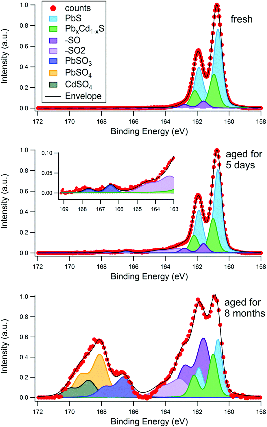 | ||
| Fig. 4 Effect of surface aging time in air on the S 2p X-ray photoelectron spectra for a 3 nm diameter PbS quantum dot with effective Cd shell thickness of 0.14 nm. The S 2p spectra were taken for the fresh sample (30 minutes of air exposure), the same sample after 5 days of ambient air exposure, and after 8 months of air exposure. The sampling depth was 1.17 nm in each case, achieved with a photon energy of 390 eV. The chemical shift for each is peak component is displayed in Table 1. | ||
| Assignment | Chemical shift from PbS (eV) | Observed chemical shift (eV) | Observed S 2p3/2 binding energy (eV) |
|---|---|---|---|
| a The S 2p spectra were calibrated to a bulk PbS S 2p3/2 component at 160.7 eV.43,44 b Species corresponding to pure CdS56 could not be fitted. The component fitted has a BE intermediate between those of PbS and CdS, see section 4.1. | |||
| Sulphur in bulk PbS | 0a | — | 160.7 |
| Sulphur in –SO/S–C/–SH | +0.9 (–SO)36/+1.1 (S–C)12/+1.2 (–SH)55 | +0.9 ± 0.1 | 161.6 ± 0.1 |
| Sulphur in –SO2 | +2.45 (ref. 34 and 36) | +2.4 ± 0.2 | 163.1 ± 0.2 |
| Sulphur in PbSO3 | +5.75 (ref. 34 and 36) | +5.75 ± 0.2 | 166.45 ± 0.2 |
| Sulphur in PbSO4 | +7.4 (ref. 36) | +7.4 ± 0.2 | 168.1 ± 0.2 |
| Sulphur in PbxCd1−xSb | +0.3b to +1 (ref. 56) | +0.3 ± 0.1 | 161 ± 0.1 |
| Sulphur in CdS | +1 (ref. 56) | —b | — |
| Sulphur in CdSO4 | +8.1 (ref. 57) | +8.1 ± 0.1 | 168.8 ± 0.1 |
It can be seen in Fig. 4 that the S 2p spectra show a strong signal in the 160–163 eV BE range, assigned to S2− in PbS/CdS, with varying amounts of smaller components to higher BE. Any structure observed between ca. 165 eV and 171 eV BE may be attributed to strongly oxidized species, such as sulphate (SVI) and sulphite (SV), with signals due to the intermediate products of oxidation (with lower S oxidation states) lying between this feature and the S2− signal.33,36 The fresh sample (after a maximum of 30 minutes of atmospheric exposure) shows little sign of oxidation, with only a small peak (with S 2p3/2 BE of 161.6 eV) visible. We assign this to species formed in the initial stages of oxidation, in particular sulphur attached to one oxygen atom (–SO),36 and –SH,33,55 although a component from the ligand S–C bond may also be present.4,12
After 5 days stored in atmosphere, small amounts of –SO2 and SO32− anions are present. After 8 months of storage a large amount of oxidation products are visible, with more SO42− anions than SO32−. A distinct CdSO4 phase is identifiable at this stage. The corresponding Pb 4f spectra for this sample also show increasing amounts of oxidation products with age (see ESI, Fig. S5†). The degradation appears first in the Pb 4f signal due to initial formation of Pb(OH)2 and PbSO3 before any sulphate appears, consistent with observations in the S 2p signal. It has been demonstrated previously that the initial reaction of PbS nanocrystals with wet air is incongruent, with oxidation of Pb (to form Pb(OH)2 and related species) occurring before significant oxidation of sulfur.33
These findings suggest that the sulphur at the surface begins to react with moisture and oxygen in the air creating –SO/–SH species first, and after more time –SO2 is produced, consistent with previous observations.33 The first oxidized sulphur anion to appear is PbSO3, which has previously been seen in the early stages of aging in PbS core only dots.12 After significant time in air lead sulphate and cadmium sulphate form. The ratio of highly oxidized Cd (CdSO4) to highly oxidized Pb (PbSO3 + PbSO4) after 8 months ageing (0.27) is less than the total Cd to total Pb ratio found at this sampling depth (about 0.5, as shown in Fig. 2), suggesting the sulphur atoms on the surface near cadmium atoms are more resistant to oxidation than those surrounded only by lead. This is consistent with observations of the passivating effect of CdS on the surface of PbS quantum dots.17,20,58,59 After 8 months’ ageing about 70% of the S 2p signal in Fig. 4 can be assigned to species considered products of the aging process (–SO/–SH, –SO2, SO32−, SO42−). Only 60% of the XPS signal at this photon energy originates from the surface atoms, suggesting that layers beneath the topmost surface layer also become oxidized too. This was examined further by depth profiling, as described below.
For samples having a small effective shell thickness, oxidized components were found in the S 2p spectrum after only half an hour exposure to air (‘fresh’). Fig. 5A shows the S 2p spectra of a sample with an effective shell thickness of 0.1 nm, as a function of sampling depth. The sulphite and sulphate components fitted to this matched with those assigned in Table 1. The ratio of the oxidized components (in this case mostly PbSO3) to PbS, is shown in Fig. 5B. Clearly the signal from oxidized S decreases with depth relative to that from PbS, i.e. the oxidized components are distributed predominantly at the CQD surface. Sulphite has been observed in the early stages of aging of PbS quantum dots,12 and is found to transform to sulphate with continuing atmospheric exposure.4
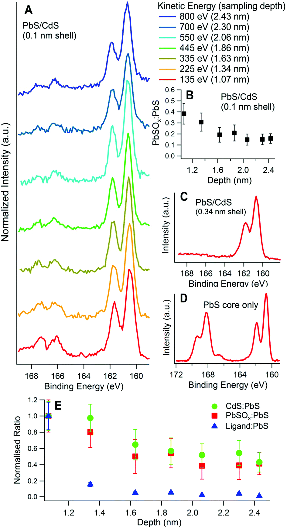 | ||
| Fig. 5 X-ray photoelectron spectra of the S 2p region for three PbS quantum dot samples with different surface passivation, but the same air exposure (up to 30 minutes) showing how the extent of surface oxidation varies in each case: (A) 5 nm diameter PbS/CdS, with 0.1 nm calculated effective shell thickness at different sampling depths, normalized to the PbS peak area; (B) the ratio of (PbSO3 + PbSO4) to PbS plotted against depth for the sample in (A); (C) 3 nm diameter PbS/CdS with 0.34 nm shell; (D) 3 nm diameter PbS core only (no CdS shell). The S 2p regions shown in (C) and (D) are obtained at 135 eV KE. Sulphite and sulphate are present in the range 165–170 eV BE. (E) Depth sensitivity plot: XPS ratios of Cd, PbSOx, and the organic ligand to PbS vs. sampling depth for the same PbS/CdS CQD (0.1 nm shell), normalized to the ratio at the lowest sampling depth. | ||
We can compare the S 2p region of the 0.1 nm-shell CQDs to those of CQDs with thicker shells, (for example a 0.34 nm shell, Fig. 5C), and with PbS core-only samples (no shell, Fig. 5D), after similar air exposure. For the thicker-shelled sample, there are clearly no detectable oxide components present in the S 2p region. In contrast, the PbS sample with no Cd shell shows much more PbSOx (x = 3, 4) relative to PbS, and most of this is sulphate (S 2p3/2 168.1 eV).
Fig. 5E shows the depth distribution of Cd, oxidized S, and the ligands in a sample with a 0.1 nm effective shell thickness. The ratio of each component to PbS is normalized to its ratio at the lowest sampling depth. The gradient of the normalized ratios vs. depth is a measure of the sensitivity of each component to changes in depth. A more negative gradient implies that the component is further from the CQD core. In Fig. 5E we see that at low sampling depths, the signal from the ligands is more strongly dependent on sampling depth than those from Cd and oxidized S. This is expected if, as we anticipate, the ligands are located on the outermost surface of the CQD. We also find that the Cd and oxidized S signals have the same sensitivity to depth, implying they are present in the same layer at the surface. This suggests that oxidized sulphur forms in the unpassivated gaps between Cd atoms in the surface.
By observing how PbS/CdS samples age with time (as shown in Fig. 4), and comparing different PbS and PbS/CdS samples (as in Fig. 5), it is evident that cation exchange of surface Pb atoms for Cd is effective in reducing the extent of surface oxidation, passivating the quantum dot surface.
3.5 Valence band photoemission
The valence band photoemission spectra of samples of varying Cd shell thickness, and after ageing are shown in Fig. 6. A low photon energy was used for all these measurements in order to maximise both the surface sensitivity and the cross section for photoemission from S 3p valence band states (see ESI†). This reduces the errors in determining the VBM position compared with conventional XPS.60 The position of the valence band maximum for each sample is listed in Table 2. Valence band maxima were determined with methods similar to those used by Chuang et al.,61 (see ESI†).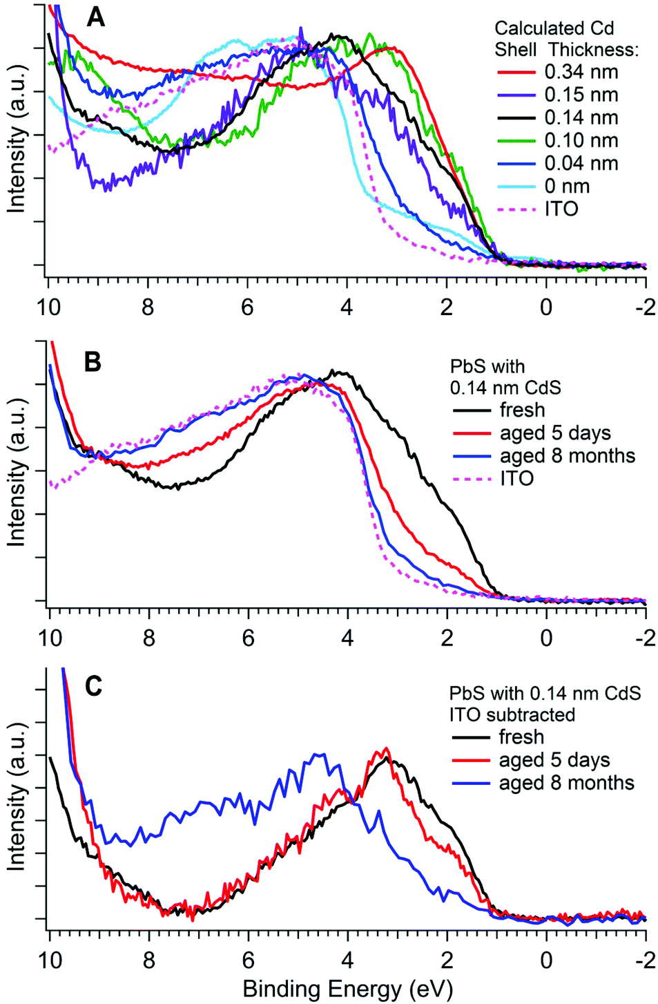 | ||
| Fig. 6 Photoemission spectra of the valence band for (A) five PbS/CdS CQD samples (after up to 30 minutes of air exposure) with different shell thicknesses (calculated from depth-profiling XPS), a PbS core only CQD (0 nm), and the ITO substrate; (B) a PbS/CdS CQD sample with a 0.14 nm thick CdS shell at various stages of aging, and the ITO substrate; (C) the same spectra shown in (B) but with the ITO valence band subtracted as described in the ESI.† All valence bands were measured with a photon energy of 370 eV. The BEs of the valence band maxima for these samples are shown in Table 2. | ||
| CdS shell thickness (nm) | Valence band maximum (eV) |
|---|---|
| 0.34 | 1.05 ± 0.10 |
| 0.15 | 0.80 ± 0.10 |
| 0.10 | 0.90 ± 0.10 |
| 0.04 | 0.85 ± 0.10 |
| 0 (PbS core only) | 0.75 ± 0.10 |
| 0.14 (fresh) | 1.00 ± 0.10 |
| 0.14 (aged 5 days) | 1.00 ± 0.10 |
| 0.14 (aged 8 months) | 1.00 ± 0.10 |
It can be seen that the electronic structure close to the valence band maximum (VBM) is strongly influenced by both CdS shell thickness and ageing. The position of the VBM for most samples is in the range 0.8–1.0 ± 0.1 eV BE (where there are no contributions from the ITO substrate), and we associate this with the intrinsic VBM of the CQDs.4,62 The position found for fresh PbS CQDs (0.75 ± 0.10 eV) is consistent with literature values for CQDs of this size.60,63–66 The valence band edge of the fresh (0.14 nm shell) sample shown in Fig. 6B & C shows two slight features, at ca. 1.8 eV and 3 eV BE, associated with the S 3p states,67 and characteristic of PbS CQDs.4,60 This structure is replicated for a number of other samples. However, it can be seen that in several samples, the intrinsic structure due to the CQDs at the valence band edge is very weak, and the edge is dominated by another feature to high BE (at ca. 3.7–3.8 eV BE). We associate this high BE feature with the products of surface ageing of the CQDs and/or the ITO substrate. The relative intensity of these two features varies with shell thickness and degree of ageing, seen clearly in comparing the spectrum of the 0.34 nm CdS shell sample with the unshelled PbS sample in Fig. 6A. In the latter case, we know that the sample is strongly oxidized at the surface (see Fig. 5D), with PbSO4 as the major oxidation product. This has a band gap of ca. 4 eV,68,69 similar to that of the ITO substrate (also ca. 4 eV), and consistent with the position of the high BE onset. Because of the similarity in band gaps of the oxidation products and of ITO, in Fig. 6C, we show data for aged samples after subtraction of the underlying ITO spectrum. Here it can be seen that the major structure at the valence band edge shifts to higher BE with aging, as the spectrum becomes dominated by oxidation products. Very similar changes are evident in Fig. 6A as the CdS shell thickness is reduced. Essentially a thick CdS shell gives a surface electronic structure characteristic of the CQD, whereas CQDs with no (or a very thin) shell have a surface band structure dominated by the wide band gap products of oxidation, introducing a barrier to charge transport.
Table 2 shows that the BE of the VBM for PbS/CdS samples does not change significantly for different CdS shell thicknesses. The VBM BE has previously been shown to be largely independent of size for 3–5 nm PbS core-only quantum dots.4,60 Similar observations have been made for other CQD systems.62 Here, the 0.10 nm shell sample, which has a total diameter of approximately 5 nm, has a similar VBM BE to the other PbS/CdS samples, which are approximately 3 nm in diameter. This suggests that the VBM position is relatively size independent in these medium-sized shelled CQD samples. The measured VBM energy has implications for the surface barrier height in shelled samples, which are discussed in section 4.2.
4. Discussion
4.1 Evidence for an alloyed shell
There are three results that suggest the cation exchange procedure produces an alloyed PbxCd1−xS shell rather than a CdS shell. First, a CdS component could not be fitted to any of the S 2p spectra taken from any PbS/CdS core/shell samples. Instead a component was fitted which lies between the binding energies of PbS and CdS. This we believe to be due to a sulphur atom surrounded by both Pb and Cd in a rock salt structure,70 illustrated in Fig. 7. Similar chemical shifts in XPS BE due to alloying have been observed in other systems.71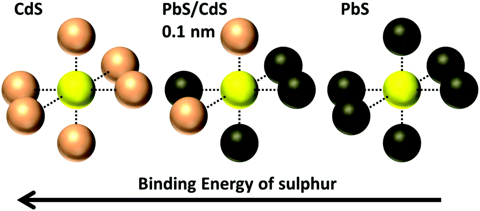 | ||
| Fig. 7 Diagram showing possible environments of lattice S and associated binding energy changes in PbxCd1−xS; CdS, PbS, and an alloyed Pb0.62Cd0.38S shell layer in a rock salt structure70 where approximately 2 out of the 6 nearest neighbour atoms are Cd, and 4 are Pb. CdS also has a rock salt structure in the CQDs.70 | ||
The second piece of evidence for alloying comes from the comparison between the shell thicknesses calculated via depth profiling XPS and TEM results.72 As an example, we take the sample with the thickest CdS shell as calculated by XPS (Fig. 3A). The bond length of CdS in the rocksalt structure is 0.265 nm.46,70 A 0.34 nm shell with no alloying would imply at least one complete monolayer of CdS has been grown. The total diameter of this CQD would be 3.8 ± 0.1 nm calculated from the 3.08 nm core (a diameter obtained from optical absorbance measurements, Fig. 1A) surrounded by the 0.34 nm shell. The TEM from this sample, Fig. 1C, shows the total size to be 3.1 ± 0.2 nm. Discrepancies of this type have also been observed in other CQD systems and are generally diagnostic of alloying.39 If the XPS-calculated total particle size is smaller than that observed in TEM, alloying in the core is indicated (as in ZnTe/ZnSe).39 The reverse observation (where the shell size calculated from XPS leads to an overall particle size larger than that observed in TEM, as here) can be explained by alloying of CdS with PbS in the shell.
The third piece of evidence supporting alloying in samples with thick shells comes from the photoemission of the valence band edges (Fig. 6A). The band gap of the PbS cores is approximately 1.4 eV,17 giving rise to the VBM feature at 0.8–1.0 ± 0.1 eV. In the case of CQDs with small effective shell thicknesses, the intrinsic structure due to the S 3p states (at ca. 1.8 eV and 3 eV BE), characteristic of PbS CQDs, is clearly visible. However, in the case of the sample with the thickest shell (0.34 nm), a broad and featureless VB edge is observed. This suggests that here the technique probes a range of S 3p energies between those characteristic of PbS and CdS, i.e. a PbxCd1−xS alloy, probably with graded composition. This is akin to the BE chemical shift we observe for the S 2p core levels, reinforcing the observations from depth profiling XPS. We conclude that (certainly for the thickest CdS shells), alloying of PbS and CdS is present in the CQD shell.
4.2 Cd – a good passivator for the PbS surface?
Our experiments provide good evidence that Cd on the PbS surface creates a better-passivated CQD than a PbS CQD without cation exchange. In Fig. 5 we compared PbS core-only CQDs to PbS/CdS CQDs with the same ligands (butylamine), and roughly the same amount of exposure to air before being measured. For the core only CQDs, very significant PbSO3 and PbSO4 is present in the S 2p spectrum compared to a cation-exchanged sample with a 0.34 nm shell which had no detectable sulphites or sulphates present (Fig. 5C & D). Because the major difference between these two samples is the surface Cd, this suggests that the Cd passivates the PbS surface well. The amount of oxidation found at the CQD surface decreases as shell thickness increases (Table S3 and Fig. S6, ESI†), becoming undetectable for shell thicknesses equivalent to less than one monolayer of CdS (Fig. S6†). In addition, we find that Cd and oxidation products show a similar depth distribution in depth profiling XPS (Fig. 5E). For most of the CQDs studied here, the effective shell thickness calculated from XPS is around 0.1–0.15 nm, significantly less than one monolayer of CdS,46 showing that a conformal CdS shell is not formed; rather, we regard the Cd as a surface ‘decoration’ which progressively displaces Pb from the surface layer as the amount of cation exchange increases. Our results show that the amount of surface oxidation decreases as this takes place, and no oxidation products are detected in the XPS of fresh samples even before the surface is fully encapsulated by a CdS shell with an effective shell thickness of more than a monolayer of CdS (Fig. S6, ESI†).This raises the question of why Cd is effective in preventing early oxidation. The free energy of reaction for formation of CdSO4 from CdS and O2 (−679 kJ mol−1) is somewhat less favourable than that for production of PbSO4 from PbS (−718 kJ mol−1),73 but this is unlikely to fully explain the marked difference in behaviour. The initial stages of degradation of PbS have been associated with an initial reaction to form Pb(OH)2:
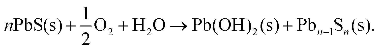 | (1) |
This creates a lead-deficient PbS phase that has been characterised by XPS.33,74 The vacancies stimulate further dissolution of the PbS, for example through reaction with protons at the surface. This initiates the oxidation of surface S2−via formation of –SH species, ultimately resulting in the sulphate layer.33 Here, we note that Pb(OH)2 is significantly more stable relative to PbS than is Cd(OH)2 relative to CdS.73 Thus we suggest that the passivating effect of Cd is associated with the lower thermodynamic stability of the initial oxidation products of Cd compared with Pb.
A PbS/CdS CQD with an effective CdS shell thickness of 0.1 nm has previously been suggested as the optimum shell thickness for a PbS/CdS CQD solar cell, giving sufficient passivation without reducing charge transport from the quantum dot.17 Our study of PbS/CdS CQDs with similar shell thicknesses shows that these CQDs have an electronic structure around the VBM which is characteristic of PbS CQDs60 (Fig. 6), i.e. the intrinsic electronic structure is barely changed by a sub-monolayer amount of CdS. Nevertheless, we observe that oxidation of the surface is significantly reduced compared with core-only PbS CQDs (Fig. 5A, C & D), and in addition, the nature of the oxidation product after a fixed air exposure is different. After short periods of air exposure, the oxidation product found on samples with a 0.1 nm shell is mostly PbSO3, which gives rise to a shallow trap state,12,75 and is not expected to greatly diminish the performance of a CQD-based photovoltaic device.13 In contrast, the main oxidation product at the same stage found for core-only PbS is PbSO4, which introduces deep trap states.12 There is a marked contrast in the electronic structure at the valence band edge (Fig. 6A), with that for the PbS core-only sample dominated by the oxidation products, whereas introduction of only a small amount of surface Cd is sufficient to retain a strong density of states at the VBM characteristic of the PbS CQD.
Thicker CdS shells, although found to have better-passivated surfaces, begin to reduce the power conversion efficiency (PCE) of solar cell devices, through a reduction in short-circuit current.17 Our observation of a VBM position that varies relatively little with shell thickness is important for understanding this behaviour. The valence band photoemission shown in Fig. 6 is sufficiently surface sensitive to probe predominantly the alloyed region in the thick-shelled (0.34 nm) sample. Despite this, we observe only a small shift (ca. 0.3 eV) of the VBM to high BE compared with the PbS core-only sample. This contrasts with the substantial VB offset of 1.73 eV expected between 3 nm PbS QDs and bulk CdS,76 an alignment that results in a CdS conduction band minimum (CBM) lower in energy than the PbS CBM. This, if replicated in the CdS shell of the CQDs would lead to no barrier to charge transport through the shell, and no clear reason for the observed loss of power conversion efficiency (PCE) with shell thickness.17 In contrast, in the shelled CQDs, our observation of only a modest change in the PbS VBM with shelling means that the CBM of a thick Cd shell is significantly higher in energy than would be expected on the basis of bulk band offsets,76–78 and above that of PbS (Fig. 8). This produces a significant barrier to charge injection into a photoanode such as ZnO, resulting in the observed loss of PCE with increasing shell thickness.
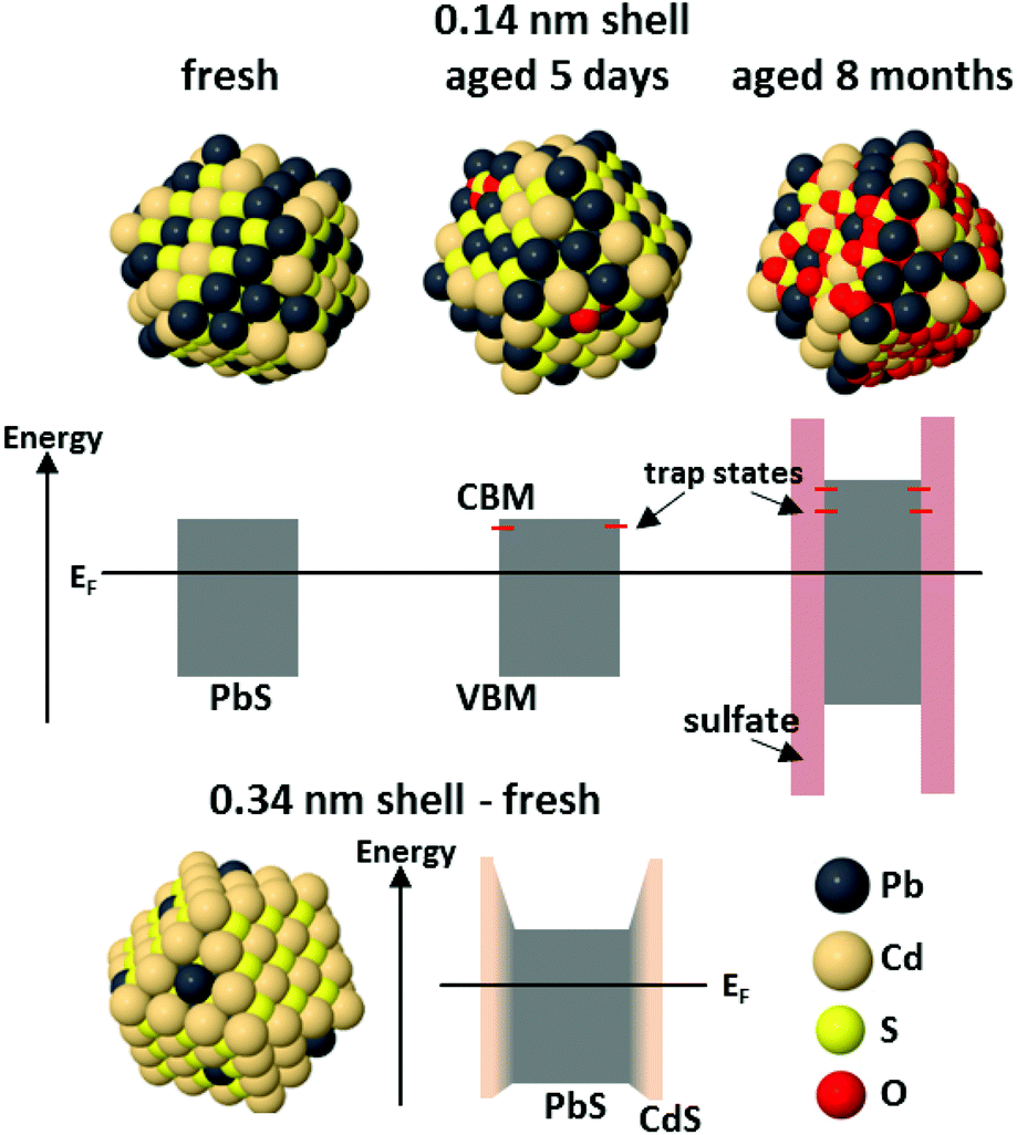 | ||
| Fig. 8 Schematic diagrams of the PbS/CdS CQD structure and band alignment for CQDs with a sub-monolayer (0.14 nm) Cd shell at three stages during aging, and for CQDs with a thicker (0.34 nm) shell. In the first case, the electronic structure of the fresh sample is not significantly changed from that of a PbS CQD. Initial oxidation to give small amounts of oxidized sulphur on the surface is accompanied by the appearance of shallow trap states below the conduction band minimum. Once the entire outside of the shell has oxidized, there is a large barrier to charge transport at the CQD surface, the core size is reduced, and deeper trap states are present due to PbSO4. For thicker-shelled CQDs, where alloying was found between the core and shell, the shell produces a barrier to charge transport at the surface. Details of the parameters used to construct this figure are given in the ESI.† | ||
Thus, a thin, sub-monolayer shell of Cd provides an optimally reduced level of surface oxidation without significant change to the electronic structure around the Fermi energy (which remains characteristic of PbS CQDs), and thus an improved PCE. However, further increase in the CdS shell thickness creates a barrier to charge transport, reducing PCE.
We have also investigated how the surface of a PbS/CdS CQD with a similar thin shell changes with exposure to air (Fig. 4). When fresh, the CQDs showed very little sign of oxidation, and after 5 days in air only a small amount of PbSO3 (introducing shallow trap states)12 was present. This relatively small amount of oxidation after 5 days in air indicates that this surface was extremely well passivated and very stable in air. However, after 8 months in air, significant amounts of sulphites and sulphates form at the surface. The total amount of sulphite and sulphates seen after this long air exposure is similar to the amount found on the PbS core-only CQD surface after half an hour of air exposure (Fig. 5D). This suggests that, although a thin CdS shell has a strong passivating effect, considerably slowing the timescales of degradation, in the longer term, the end product of degradation is PbSO4 (introducing deep trap states) as previously seen in PbS core-only CQDs.4 It is noticeable, however, that even after 8 months in air, conversion of PbSO3 to PbSO4 is not complete in the shelled sample (Fig. 4 and S5 in ESI†). The combination of cadmium passivation with halide passivation could provide the optimum passivation strategy for PbS CQDs developed for solar cell use,17 with minimum disruption to the electronic structure.
5. Conclusions
SR-excited depth profiling XPS enables us to present a detailed atomic-level description of the passivating action of Cd on PbS CQDs. We show that Cd introduced into PbS CQDs by cation exchange is localized at the surfaces of the CQDs. The effective CdS shell thickness is calculated from XPS and found to correlate well with both the extent of oxidation and the electronic structure at the VBM. A sub-monolayer surface ‘decoration’ of Cd is found to be effective in passivating the CQDs, leading to low rates of initial oxidation, and the production predominantly of PbSO3 (associated with shallow traps) rather than PbSO4 (associated with deep traps).12,75 Conversion of PbSO3 to PbSO4 is incomplete even after prolonged oxidation, in contrast to unshelled CQDs. The CdS shell was found to be alloyed with PbS, most evident when the shell thickness is greater than one monolayer of CdS. Thicker shells passivate the CQD surfaces better, showing lower amounts of oxidation after the same exposure times. The tunability provided by SR enables us to demonstrate that the oxidation products are localized at the CQD surface and have a similar depth distribution to the surface Cd. We show that the chemical products of early oxidation are progressively eliminated as Cd replaces Pb at the surface. We associate this with the lower thermodynamic stability of the initial oxidation products of Cd compared with Pb.We find that the electronic structure close to the valence band edge in well-passivated samples is dominated by structure intrinsic to the CQD, with a VBM in the range 0.8–1.0 ± 0.1 eV BE. As oxidation proceeds, this becomes dominated by high binding energy features due to the wide band gap products of oxidation. The part of the VBM structure intrinsic to the CQD is characteristic of PbS for shell thicknesses up to 0.15 nm, and is perturbed in only a minor way when a thicker shell is grown. The energy position of this VBM has the result that the CBM at the surface is significantly higher in energy than would be expected on the basis of bulk band offsets when a thick CdS shell is grown. This produces the barrier to charge transport noted by us when these CQDs were incorporated into solar test devices.17
All shelled samples showed significantly less surface oxidation than PbS CQDs with no shell. The depth-profiling results reported here give strong evidence that cation-exchanged PbS/CdS CQDs are more air stable than PbS CQDs when even sub-monolayer amounts of Cd are present on the surface. The optimum shell thickness (of around 0.1 nm) found for maximised PCE17 corresponds to the best passivation that can be achieved without modification of the electronic structure so as to introduce a significant barrier to charge transport at the surface. These studies reveal that the energy-level alignments at PbS/CdS CQD surfaces differ from those expected on the basis of bulk band offsets, and are strongly affected by oxidation products. In turn, this influences the height of the barrier to charge transport at the CQD surfaces. This emphasizes the need for more nm-scale studies of surfaces and interfaces in CQD-based devices.
Acknowledgements
The research leading to these results received funding from the European Community's Seventh Framework Programme (FP7/2007–2015) under grant agreements no. 226716 and 288879, allowing access to Synchrotron SOLEIL, Elettra and Max-Lab. We thank the CNR-IOM technician, F. Salvador and P. Bertoch. Work was also supported by EPSRC (UK) under grant no. EP/K008544/1. The data associated with this paper are openly available from The University of Manchester eScholar Data Repository: DOI: 10.15127/1.305124.References
- M. Liu, F. P. G. de Arquer, Y. Li, X. Lan, G. H. Kim, O. Voznyy, L. K. Jagadamma, A. S. Abbas, S. Hoogland, Z. Lu, J. Y. Kim, A. Amassian and E. H. Sargent, Adv. Mater., 2016, 28, 4142–4148 CrossRef CAS PubMed.
- M. Graetzel, R. A. J. Janssen, D. B. Mitzi and E. H. Sargent, Nature, 2012, 488, 304–312 CrossRef CAS PubMed.
- W. Shockley and H. J. Queisser, J. Appl. Phys., 1961, 32, 510–519 CrossRef CAS.
- S. J. O. Hardman, D. M. Graham, S. K. Stubbs, B. F. Spencer, E. A. Seddon, H.-T. Fung, S. Gardonio, F. Sirotti, M. G. Silly, J. Akhtar, P. O'Brien, D. J. Binks and W. R. Flavell, Phys. Chem. Chem. Phys., 2011, 13, 20275–20283 RSC.
- A. G. Midgett, J. M. Luther, J. T. Stewart, D. K. Smith, L. A. Padilha, V. I. Klimov, A. J. Nozik and M. C. Beard, Nano Lett., 2013, 13, 3078–3085 CrossRef CAS PubMed.
- X. F. Shi, X. Y. Xia, G. W. Cui, N. Deng, Y. Q. Zhao, L. H. Zhuo and B. Tang, Appl. Catal., B, 2015, 163, 123–128 CrossRef CAS.
- R. J. Ellingson, M. C. Beard, J. C. Johnson, P. Yu, O. I. Micic, A. J. Nozik, A. Shabaev and A. L. Efros, Nano Lett., 2005, 5, 865–871 CrossRef CAS PubMed.
- C. Smith and D. J. Binks, Nanomaterials, 2014, 4, 19–45 CrossRef PubMed.
- E. Tekin, P. J. Smith and U. S. Schubert, Soft Matter, 2008, 4, 703–713 RSC.
- J. Zhang, R. Li, W. Sun, Q. Wang, X. Miao and D. Zhang, J. Mater. Chem. C, 2014, 2, 4442–4448 RSC.
- H. Choi, J. Ko, Y. Kim and S. Jeong, J. Am. Chem. Soc., 2013, 135, 5278–5281 CrossRef CAS PubMed.
- J. Tang, L. Brzozowski, D. A. R. Barkhouse, X. Wang, R. Debnath, R. Wolowiec, E. Palmiano, L. Levina, A. G. Pattantyus-Abraham, D. Jamakosmanovic and E. H. Sargent, ACS Nano, 2010, 4, 869–878 CrossRef CAS PubMed.
- J. Tang, K. W. Kemp, S. Hoogland, K. S. Jeong, H. Liu, L. Levina, M. Furukawa, X. Wang, R. Debnath, D. Cha, K. W. Chou, A. Fischer, A. Amassian, J. B. Asbury and E. H. Sargent, Nat. Mater., 2011, 10, 765–771 CrossRef CAS PubMed.
- Z. Ning, O. Voznyy, J. Pan, S. Hoogland, V. Adinolfi, J. Xu, M. Li, A. R. Kirmani, J.-P. Sun, J. Minor, K. W. Kemp, H. Dong, L. Rollny, A. Labelle, G. Carey, B. Sutherland, I. Hill, A. Amassian, H. Liu, J. Tang, O. M. Bakr and E. H. Sargent, Nat. Mater., 2014, 13, 822–828 CrossRef CAS PubMed.
- X. Lan, O. Voznyy, A. Kiani, F. P. García de Arquer, A. S. Abbas, G.-H. Kim, M. Liu, Z. Yang, G. Walters, J. Xu, M. Yuan, Z. Ning, F. Fan, P. Kanjanaboos, I. Kramer, D. Zhitomirsky, P. Lee, A. Perelgut, S. Hoogland and E. H. Sargent, Adv. Mater., 2015, 28, 299–304 CrossRef PubMed.
- Y. Cao, A. Stavrinadis, T. Lasanta, D. So and G. Konstantatos, Nat. Energy, 2016, 1, 16035 CrossRef CAS.
- D. C. J. Neo, C. Cheng, S. D. Stranks, S. M. Fairclough, J. S. Kim, A. I. Kirkland, J. M. Smith, H. J. Snaith, H. E. Assender and A. A. R. Watt, Chem. Mater., 2014, 26, 4004–4013 CrossRef CAS.
- B. A. Gonfa, M. R. Kim, N. Delegan, A. C. Tavares, R. Izquierdo, N. Wu, M. A. El Khakani and D. Ma, Nanoscale, 2015, 10039–10049 RSC.
- L.-H. Lai, L. Protesescu, M. V. Kovalenko and M. A. Loi, Phys. Chem. Chem. Phys., 2014, 16, 736–742 RSC.
- H. Zhao, M. Chaker, N. Wu and D. Ma, J. Mater. Chem., 2011, 21, 8898–8904 RSC.
- D. C. J. Neo, S. D. Stranks, G. E. Eperon, H. J. Snaith, H. E. Assender, A. R. Andrew, D. C. J. Neo, S. D. Stranks, G. E. Eperon, H. J. Snaith, H. E. Assender and A. A. R. Watt, Appl. Phys. Lett., 2015, 107, 103902 CrossRef.
- M. J. Speirs, D. M. Balazs, H.-H. Fang, L.-H. Lai, L. Protesescu, M. V. Kovalenko and M. A. Loi, J. Mater. Chem. A, 2015, 3, 1450–1457 CAS.
- M. P. Seah and W. A. Dench, Surf. Interface Anal., 1979, 1, 2–11 CrossRef CAS.
- B. F. Spencer, M. A. Leontiadou, P. C. J. Clark, A. Williamson, M. G. Silly, F. Sirotti, S. M. Fairclough, D. C. J. Neo, A. A. R. Watt and W. R. Flavell, Appl. Phys. Lett., 2016, 108, 91603 CrossRef.
- R. C. Page, D. Espinobarro-Velazquez, M. A. Leontiadou, C. Smith, E. A. Lewis, S. J. Haigh, C. Li, H. Radtke, A. Pengpad, F. Bondino, E. Magnano, I. Pis, W. R. Flavell, P. O'Brien and D. J. Binks, Small, 2015, 11, 1548–1554 CrossRef CAS PubMed.
- W. H. Doh, V. Papaefthimiou, T. Dintzer, V. Dupuis and S. Zafeiratos, J. Phys. Chem. C, 2014, 118, 26621–26628 CAS.
- J. Pichaandi, G. K. Das, N. J. J. Johnson, T. Regier and F. C. J. M. van Veggel, J. Phys. Chem. C, 2014, 118, 21639–21646 CAS.
- A. G. Shard, J. Wang and S. J. Spencer, Surf. Interface Anal., 2009, 41, 541–548 CrossRef CAS.
- B. F. Spencer, M. J. Cliffe, D. M. Graham, S. J. O. Hardman, E. A. Seddon, K. L. Syres, A. G. Thomas, F. Sirotti, M. G. Silly, J. Akhtar, P. O'Brien, S. M. Fairclough, J. M. Smith, S. Chattopadhyay and W. R. Flavell, Surf. Sci., 2015, 641, 320–325 CrossRef CAS.
- H. Borchert, S. Haubold, M. Haase, H. Weller, C. McGinley, M. Riedler and T. Möller, Nano Lett., 2002, 2, 151–154 CrossRef CAS.
- P. K. Santra, R. Viswanatha, S. M. Daniels, L. Pickett, J. M. Smith, P. O'Brien and D. D. Sarma, J. Am. Chem. Soc., 2009, 131, 470–477 CrossRef CAS PubMed.
- D. D. Sarma, P. K. Santra, S. Mukherjee and A. Nag, Chem. Mater., 2013, 25, 1222–1232 CrossRef CAS.
- D. J. H. Cant, K. L. Syres, P. J. B. Lunt, H. Radtke, J. Treacy, P. J. Thomas, E. A. Lewis, S. J. Haigh, P. O. Brien, K. Schulte, F. Bondino, E. Magnano and W. R. Flavell, Langmuir, 2015, 31, 1445–1453 CrossRef CAS PubMed.
- A. Lobo, T. Möller, M. Nagel, H. Borchert, S. G. Hickey and H. Weller, J. Phys. Chem. B, 2005, 109, 17422–17428 CrossRef CAS PubMed.
- A. G. Shard, J. Phys. Chem. C, 2012, 116, 16806–16813 CAS.
- L. V. Yashina, A. S. Zyubin, R. Püttner, T. S. Zyubina, V. S. Neudachina, P. Stojanov, J. Riley, S. N. Dedyulin, M. M. Brzhezinskaya and V. I. Shtanov, Surf. Sci., 2011, 605, 473–482 CrossRef CAS.
- M. A. Hines and G. D. Scholes, Adv. Mater., 2003, 15, 1844–1849 CrossRef CAS.
- M. S. Neo, N. Venkatram, G. S. Li, W. S. Chin and W. Ji, J. Phys. Chem. C, 2010, 114, 18037–18044 CAS.
- S. M. Fairclough, E. J. Tyrrell, D. M. Graham, P. J. B. Lunt, S. J. O. Hardman, A. Pietzsch, F. Hennies, J. Moghal, W. R. Flavell, A. a. R. Watt and J. M. Smith, J. Phys. Chem. C, 2012, 116, 26898–26907 CAS.
- W. Zhang, G. Chen, J. Wang, B. C. Ye and X. Zhong, Inorg. Chem., 2009, 48, 9723–9731 CrossRef CAS PubMed.
- 2011 .
- J. J. Yeh, Atomic Calculation of Photoionization Cross-Sections and Asymmetry Parameters, Gordon and Breach Science Publishers, Langhorne, PE, 1993 Search PubMed.
- G. Wittstock, I. Kartio, D. Hirsch, S. Kunze and R. Szargan, Langmuir, 1996, 12, 5709–5721 CrossRef CAS.
- A. H. Ip, S. M. Thon, S. Hoogland, O. Voznyy, D. Zhitomirsky, R. Debnath, L. Levina, L. R. Rollny, G. H. Carey, A. Fischer, K. W. Kemp, I. J. Kramer, Z. Ning, A. J. Labelle, K. W. Chou, A. Amassian and E. H. Sargent, Nat. Nanotechnol., 2012, 7, 577–582 CrossRef CAS PubMed.
- I. Moreels, K. Lambert, D. Smeets, D. De Muynck, T. Nollet, J. C. Martins, F. Vanhaecke, A. Vantomme, C. Delerue, G. Allan and Z. Hens, ACS Nano, 2009, 3, 3023–3030 CrossRef CAS PubMed.
- C. J. M. Rooymans, Phys. Lett., 1963, 4, 186–187 CrossRef CAS.
- L. A. King and D. J. Riley, J. Phys. Chem. C, 2012, 116, 3349–3355 CAS.
- J. B. Sambur, S. C. Riha, D. Choi and B. A. Parkinson, Langmuir, 2010, 26, 4839–4847 CrossRef CAS PubMed.
- M. Tagliazucchi, D. B. Tice, C. M. Sweeney, A. J. Morris-Cohen and E. A. Weiss, ACS Nano, 2011, 5, 9907–9917 CrossRef CAS PubMed.
- Q. Dai, J. Chen, L. Lu, J. Tang and W. Wang, Appl. Phys. Lett., 2013, 102, 203904 CrossRef.
- M. P. Seah and I. S. Gilmore, Surf. Interface Anal., 2001, 31, 835–846 CrossRef CAS.
- S. Tanuma, C. J. Powell and D. R. Penn, Surf. Interface Anal., 1994, 21, 165–176 CrossRef CAS.
- S. Tanuma, C. J. Powell and D. R. Penn, Surf. Interface Anal., 2003, 35, 268–275 CrossRef CAS.
- C. J. Powell and A. Jablonski, NIST Electron Inelastic Mean Free Path Database, National Institute of Standards and Technology, Gaithersburg, 2010 Search PubMed.
- A. J. Leavitt and T. P. Beebe, Surf. Sci., 1994, 314, 23–33 CrossRef CAS.
- X. R. Yu, F. Liu, Z. Y. Wang and Y. Chen, J. Electron Spectrosc. Relat. Phenom., 1990, 50, 159–166 CrossRef CAS.
- H. L. Pushpalatha and R. Ganesha, Int. J. ChemTech Res., 2015, 7, 2171–2175 CAS.
- H. Zhao, M. Chaker and D. Ma, J. Mater. Chem., 2011, 21, 17483–17491 RSC.
- A. Manjceevan and J. Bandara, Sol. Energy Mater. Sol. Cells, 2016, 147, 157–163 CrossRef CAS.
- E. M. Miller, D. M. Kroupa, J. Zhang, P. Schulz, A. R. Marshall, A. Kahn, S. Lany, J. M. Luther, M. C. Beard, C. L. Perkins and J. Van De Lagemaat, ACS Nano, 2016, 10, 3302–3311 CrossRef CAS PubMed.
- C.-H. M. Chuang, P. R. Brown, V. Bulović and M. G. Bawendi, Nat. Mater., 2014, 13, 796–801 CrossRef CAS PubMed.
- B. Carlson, K. Leschkies, E. S. Aydil and X. Y. Zhu, J. Phys. Chem. C, 2008, 112, 8419–8423 CAS.
- J. Akhtar, M. Azad Malik, P. O'Brien, K. G. U. Wijayantha, R. Dharmadasa, S. J. O. Hardman, D. M. Graham, B. F. Spencer, S. K. Stubbs, W. R. Flavell, D. J. Binks, F. Sirotti, M. El Kazzi and M. Silly, J. Mater. Chem., 2010, 20, 2336–2344 RSC.
- T. G. Kim, H. Choi, S. Jeong and J. W. Kim, J. Phys. Chem. C, 2014, 118, 27884–27889 CAS.
- P. R. Brown, D. Kim, R. R. Lunt, N. Zhao, M. G. Bawendi, J. C. Grossman and V. Bulovi, ACS Nano, 2014, 8, 5863–5872 CrossRef CAS PubMed.
- B. P. Bloom, M. N. Mendis, E. Wierzbinski and D. H. Waldeck, J. Mater. Chem. C, 2016, 4, 704–712 RSC.
- T. Ollonqvist, T. Kanrila, M. Isokallio, M. Punkkinen and J. Vayrynen, J. Electron Spectrosc. Relat. Phenom., 1995, 76, 729–734 CrossRef CAS.
- A. Amat, C. Miliani and S. Fantacci, RSC Adv., 2016, 6, 36336–36344 RSC.
- I. A. Kamenskikh, M. Kirm, V. N. Kolobanov, V. V. Mikhailin, P. A. Orekhanov, I. N. Shpinkov, D. A. Spassky, A. N. Vasil'ev, B. I. Zadneprovsky and G. Zimmerer, IEEE Trans. Nucl. Sci., 2001, 48, 2324–2329 CrossRef CAS.
- R. T. Lechner, G. Fritz-Popovski, M. Yarema, W. Heiss, A. Hoell, T. U. Schu, D. Primetzhofer, M. Eibelhuber and O. Paris, Chem. Mater., 2014, 26, 5914–5922 CrossRef CAS PubMed.
- J.-G. Song, G. H. Ryu, S. J. Lee, S. Sim, C. W. Lee, T. Choi, H. Jung, Y. Kim, Z. Lee, J.-M. Myoung, C. Dussarrat, C. Lansalot-Matras, J. Park, H. Choi and H. Kim, Nat. Commun., 2015, 6, 7817 CrossRef PubMed.
- C. T. Smith, M. A. Leontiadou, P. C. J. Clark, C. Lydon, N. Savjani, B. F. Spencer, W. R. Flavell, P. O'Brien and D. J. Binks, J. Phys. Chem. C, 2017, 121, 2099–2107 CAS.
- CRC Handbook of Chemistry and Physics, Internet Version, ed. W. M. Haynes, CRC Press, Boca Raton, FL, 97th edn, 2016 Search PubMed.
- V. Malgras, A. Nattestad, Y. Yamauchi, S. X. Dou and J. H. Kim, Nanoscale, 2015, 7, 5706–5711 RSC.
- G. Konstantatos and E. H. Sargent, Appl. Phys. Lett., 2007, 91, 173505 CrossRef.
- K. P. Bhandari, H. Choi, S. Jeong, H. Mahabaduge and R. J. Ellingson, Appl. Phys. Lett., 2014, 105, 131604 CrossRef.
- W. Mönch, Appl. Phys. Lett., 1998, 72, 1899–1901 CrossRef.
- L. D. Zhao, J. He, S. Hao, C. I. Wu, T. P. Hogan, C. Wolverton, V. P. Dravid and M. G. Kanatzidis, J. Am. Chem. Soc., 2012, 134, 16327–16336 CrossRef CAS PubMed.
Footnotes |
| † Electronic supplementary information (ESI) available: Details of ligand exchange procedures, extracting elemental ratios from XPS, sampling depth and shell thickness calculations, comparison of XPS-determined and absorption-determined shell thickness, spectra showing the ligands in bound and unbound states and the effect of aging on the Pb 4f spectra, assignment tables of chemical species found in XPS, depth sensitivities of Cd and oxide on the surface, details on the valence band alignment, details of the parameters used to construct Fig. 8. See DOI: 10.1039/c7nr00672a |
| ‡ Present address: School of Materials, The University of Manchester, Manchester M13 9PL, UK. |
| § Present address: Manchester Institute of Biotechnology and the Photon Science Institute, The University of Manchester, Manchester M13 9PL, UK. |
| ¶ Present address: Department of Chemistry, University of California, Irvine, Irvine, California 92697, USA. |
| || Present address: Department of Physics, King's College London, Strand, London WC2R 2LS, UK. |
| This journal is © The Royal Society of Chemistry 2017 |