
 Open Access Article
 This Open Access Article is licensed under a
 Creative Commons Attribution 3.0 Unported Licence
Atomically-resolved edge states on surface-nanotemplated graphene explored at room temperature†
Pablo
Merino‡
*a,
Hernán
Santos
b,
Anna L.
Pinardi
c,
Leonor
Chico
c and
José A.
Martin-Gago
ac
aCentro de Astrobiología, INTA-CSIC, Carretera de Ajalvir km. 4, E-28850, Torrejón de Ardoz, Spain. E-mail: p.merino@fkf.mpg.de
bDepartamento de Física Fundamental, Universidad Nacional de Educación a Distancia, E-28040, Madrid, Spain
cInstituto de Ciencia de Materiales de Madrid, CSIC, c/Sor Juana Inés de la Cruz 3, E28049, Madrid, Spain
First published on 14th February 2017
Abstract
Graphene edges present localized electronic states strongly depending on their shape, size and border configuration. Chiral- or zigzag-ended graphene nanostructures develop spatially and spectrally localized edge states around the Fermi level; however, atomic scale investigations of such graphene terminations and their related electronic states are very challenging and many of their properties remain unexplored. Here we present a combined experimental and theoretical study on graphene stripes showing strong metallic edge states at room temperature. By means of scanning tunneling microscopy, we demonstrate the use of vicinal Pt(111) as a template for the growth of graphene stripes and characterize their electronic structure. We find the formation of a sublattice localized electronic state confined on the free-standing edges of the graphene ribbons at energies close to the Fermi level. These experimental results are reproduced and understood with tight-binding and ab initio calculations. Our results provide a new way of synthesizing wide graphene stripes with zigzag edge termination and open new prospects in the study of valley and spin phenomena at their interfaces.
Introduction
The edges of graphene exhibit unique physical and chemical properties that confer an extra appeal to this fascinating 2D material. Depending on the size and the shape of the graphene sheet and its edge geometry, graphene interfaces can present localized metallic or semiconducting electronic states. A number of edge terminations have been conceived: zigzag, armchair, chiral, cove, cape and, more generally, disordered edges have been theoretically and experimentally addressed.1–4 Because of their relative simplicity, graphene stripes of nanometer width and quasi-one-dimensional behavior are an excellent playground for the study of their edge states.5–11 Pioneering theoretical work predicted that zigzag-ended graphene borders should develop strong edge states near the Fermi level, while armchair-ended interfaces do not.12 These states have been predicted to have a magnetic character and spin-polarized currents13,14 and represent a possible source of carbon-based magnetism.From the experimental viewpoint, atomically-precise control of the edge geometry and characterization of the interface electronic structure is a challenging task.15,16 Classical graphene production methods have been optimized for obtaining large-area crystalline mesoscopic samples; exfoliated,17 or epitaxial18 graphene sheets, while showing low density of defects in the basal plane, they rarely present atomically clean edges but rather a combination of zigzag, armchair and amorphous regions that merges and obscures the electronic properties of the borders. Different approaches have been put forward to obtain crystalline graphene edges and investigate their edge states. Patterning by nanolithography methods19 or by scanning probe microscopy manipulations20 has been tested and graphene edges successfully engineered; but with resolutions still limited to some unsatisfactory few nm. Unzipping of carbon nanotubes (CNTs) by chemical treatments resulted in regions of atomically precise chiral edges, showing that the unzipping direction lies close to the axial direction of the CNTs.21,22 Alternatively to top-down approaches, bottom-up efforts based on the surface-catalyzed reaction of molecular precursors have recently emerged. This methodology proved very successful for obtaining atomically-precise graphene edges;5,23,24 yet the resulting graphene nanoribbons (GNRs) are limited to “ultra-narrow” widths making their electronic structure complicated to address.25,26
Despite the large heed paid to graphene edge states, experimental evidence about their spatial and spectral localization remains scarce. Only a limited number of studies, prominently by the use of scanning tunneling microscopy and spectroscopy (STM-STS),22,25,26 have been able to characterize the electronic structure of graphene edges with sub-nm and meV resolution. This lack of experimental evidence is mainly due to the trouble for obtaining graphene geometries presenting strong edge phenomena. Here we show that robust edge states can be obtained in graphene stripes grown on vicinal Pt surfaces and characterized with atomic precision. Using vicinal Pt(111) surfaces and C60-fullerenes as carbon-containing molecular precursors, we grow graphene stripes of an average width of 10 nm and a few hundreds of nm long. Under these growth conditions, one of the edges of the stripe appears to be freestanding and presents an average chirality of (3,1), while the opposite edge is chemically bonded to a metal step of the substrate. Atomically resolved STM images of the freestanding edges show the presence of a region of enhanced conductivity at the edge atoms, suggesting the presence of localized edge states. Ab initio and tight-binding simulations further demonstrate the appearance of a spectrally and spatially sharp edge state localized at the Fermi level. Measurements of the intensity of the edge state at room temperature for different bias voltages further corroborate the metallic nature of the state.
Results and discussion
Fig. 1a shows a 3D representation of a 50 × 50 nm2 topographic STM image of the graphene stripes grown on vicinal Pt(111) using C60 as molecular precursors. The surface is heavily stepped and five parallel terraces of an average width of 10 nm run along the image. All the STM images presented throughout the manuscript are obtained by scanning, descending the tip from upper terraces to lower terraces. The height difference between adjacent terraces reveals the presence of multiple atomically-high (with a0 = 2.27 Å) bunched steps. The process of step bunching is well known on Pt(111) vicinal surfaces,27 and can be triggered by high temperature annealing,28 or after chemical reactions taking place at the reactive kink position.29 Here, the use of C60 as a graphene precursor and/or the high temperatures used for molecular decomposition and graphene growth induce step bunching in packets of two or three single atomic steps.30 | ||
| Fig. 1 (a) Pseudo-3D topography map of the stepped Pt(111) surface covered with single layer graphene. 50 × 50 nm2, 10 mV, 2 nA. The mean step height corresponds to three single Pt steps (a0) (represented by arrows) (b) atomically resolved STM topography image of a step like the ones presented in (a). 13.5 × 13.5 nm2, 400 mV, 3.3 nA. The line running vertically across the image demonstrates that graphene does not grow in a carpet-like configuration but presents discontinuity at the step position due to the large height of the steps (6.6 Å). Inset: STM image of the moiré superstructure (3 × 3)G or (√7 × √7)R19°; 2 × 2 nm2, −100 mV, 4.2 nA. (c) Ball-and-stick scheme of a bunched step like the one presented in (b). Graphene covers both terraces; in the upper terrace it ends in a border-like edge. In the lower terrace the graphene grows attached to the lower Pt atoms of the step in a step-like configuration. | ||
Fig. 1b shows one of the multiple steps in detail. The left part is a terrace which appears raised up 6.6 Å with respect to the terrace appearing in pink on the right part of the image. Both terraces are covered with graphene presenting a (√7 × √7)R19° moiré superstructure (see the lower right inset for details of the moiré).31,32 At the relative high voltage bias (400 mV) used to measure Fig. 1b, the graphene discontinuity between both terraces is clearly visible as a stripe of amorphous configuration in the middle of the image. This behavior of graphene grown on vicinal Pt(111) is in contrast to the observation of graphene growing in a carpet-like configuration over step edges discovered on other transition metals like Ir(111)33 or Ru(0001).34 The irregular region appearing in the middle of the image corresponds to a small region where the metal substrate can be imaged between the upper and lower graphene terraces. The height difference between both terraces makes it very difficult to obtain details of this intermediate sloppy region. There is also a linear region parallel to the step on the lower terrace where graphene appears to be combed. This effect might arise due to the compression exerted on the graphene layer by the substrate, due to the difference in the thermal expansion coefficients after the cooling process. We have displayed in Fig. 1c, a ball-and-stick model of the atomic configuration proposed for a step like the one presented in Fig. 1b. The upper terrace is covered with graphene finishing in a step-like configuration35 which leaves the last atomic rows of graphene “flying freely”, while the lower terrace is chemically bound to the lower Pt step in a border-like configuration35 where the last C atoms are covalently bonded to the first atoms of Pt. We observe that no interface-localized states appear at the graphene/Pt contact region. Such covalently bonded edges can, however, present sublattice-localized electronic states of moderate intensity if the graphene layer remains flat and is not combed like in the present case.36
To enhance the resolution of the images, we have recorded quasi-constant height STM images. In this mode, we represent current error maps where the difference between the current setpoint and the measured current for every pixel during conventional STM operations with feedback conditions “on” is plotted. Both STM topographic and current error maps show the same atomic scale features, but the latter present enhanced resolution.36 When analyzing the absolute current error map obtained simultaneously with the topographic images at bias close to the Fermi level a striking effect shows up. Although restrictive feedback conditions were used to scan the highly faceted surface, the microscope could not keep the current setpoint when the tip scanned over the step-like graphene edges, leading to a high value of the current. Since the images were obtained scanning the tip from the upper to the lower terrace any possible feedback maladjustment effects can be precluded to appear in the step-like edges of graphene (see the ESI† for raw data and further details). The effect can be observed in Fig. 2; the green lines running vertically correspond to regions with currents highly exceeding the 2 nA setpoint (see the scale bars insets). This exceptionally confined current raise is a clear indication of the presence of additional sharply localized states opening new channels for the electrons to tunnel, enhancing the conductivity of the surface on these positions of the surface. As noticed in Fig. 2a, the localized states are situated at the end of the step-like edges of graphene forming linear structures running parallel to the steps. The 1D states appear extended over the full length of the edges, albeit they present heterogeneities; the origin of this effect will be discussed in detail later. The current raise can also be observed in the topographic maps as a protrusion appearing on top of the steps (see the 3D profile of Fig. 1a), as the tip retracts in these points to decrease the value of the current to the setpoint parameter, giving the impression of a topographic elevation.
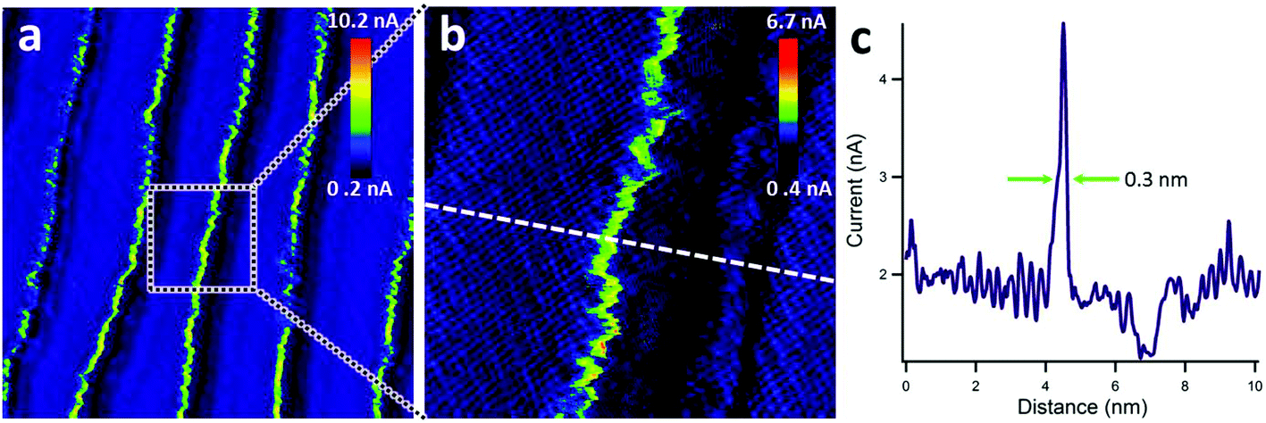 | ||
| Fig. 2 (a) Current error map (see Methods) acquired simultaneously with Fig. 1(a). The green lines correspond to spatially localized electronic states that open new channels for the conductance. The color scale of the current is presented in the upper corner of the image. 50 × 50 nm2, −10 mV, 2 nA. (b) Atomically resolved current error map corresponding to the region enclosed in a square in (a) 10 × 10 nm2, −10 mV, 2 nA. (c) Profile of the line marked in (b). The small corrugation in the baseline of 2 nm reflects the atomic resolution. The big spike in the profile, width 0.3 nm, is located at the end of the graphene upper terrace. | ||
Fig. 2b shows a high resolution STM current error map where graphene is atomically resolved in both the upper and the lower terraces. The tunneling parameters of this image are −10 mV, and 2 nA. These bias conditions were chosen to maximize the atomic resolution which is enhanced for G/Pt(111) when scanning at high currents with voltages near the Fermi level (EF). The profile of the absolute value of the current for the trajectory marked with a white dashed line in Fig. 2b is presented in Fig. 2c. As expected, the baseline of the profile corresponds to 2 nA and the small scale undulations reflect current heterogeneities resulting from the positions of the atoms in the graphene lattice.37 The sharp spike in the current, which reaches up to 5 nA in the current profile, correlates with the atomic position of the graphene edge in the step-like configuration. This spike reflects the region – only one or two graphene unit cells – of enhanced conductivity and can be regarded as a real-space measurement of the edge-state of the graphene stripe.
To better understand the origin of the experimentally observed edge states, we have performed calculations of a wide region of a single chiral edge with unsaturated carbon atoms in a semi-infinite graphene within the tight-binding approach. In Fig. 3a, we present an experimental image of a region of a step-like edge where the atomic positions of the carbon honeycomb lattice can be visualized. In Fig. 3b, we present the experimental determination of the atomic positions of graphene by overlaying a white honeycomb lattice. The graphene edge at this region has an average chirality of (3,1), but also presents regions with (4,1) cells. As a general tendency, the edges formed with our experimental protocol maximize the zigzag termination and avoid the formation of extended armchair regions. The real space weight of the density of states (DOS) at the Fermi level resulting from tight-binding calculations of a semi-infinite ribbon is presented in Fig. 3c. The electronic structure has been weighted by the pz orbitals and plotted in green on top of the unit cell used for the simulation. For the energy window considered here, only the pz orbitals are relevant. The results of our simulations show that the DOS is mainly localized in one of the two graphene sublattices, while the other presents a negligible contribution. In particular, only the sublattice that exposes their last atoms to the vacuum interface (C atoms with atomic coordination 2) contributes to the DOS (see Fig. 3c). The intensity of state decays very rapidly when moving away from the edge. Notice that, contrary to GNRs, for which two edge states should appear, we have only one maximum in the intensity, indicating that they can be regarded as isolated graphene edge states. Interestingly, in Fig. 3a, the spatial modulation of the experimental electronic state at the edge can be traced down to the atomic scale. Inspection of the intensity of the edge state reveals the presence of maxima in the current error maps spatially correlated with atoms belonging to one of the hexagonal sublattices of graphene (see the overlaid honeycomb lattice in Fig. 3b), in good agreement with the theory. Although we have not used Tersoff–Hamann or any other advanced STM simulation methods for reproducing Fig. 3c, the agreement between theory and experiments is rather good.
 | ||
| Fig. 3 (a) Ultrahigh resolution current error map of a step-like edge of graphene 1.8 × 2.9 nm2, −3 mV, 2 nA. (b) The same image as in (a) where a honeycomb lattice schematically representing graphene has been overlaid. The honeycomb lattice observed in (a) does not correspond with the real graphene lattice but rather to only one of the sublattices. (c) Calculated real space density of states of a semi-infinite graphene slab with an edge termination corresponding to (a) and (b). (d) Energy spectrum of a (3,1) GNR. The state seen at the Fermi level corresponds to the edge state discussed in the text. | ||
The band dispersion of a (3,1) ended semi-infinite 2D sheet is presented in Fig. 3d. The zero-energy flat band at the Fermi level (green line in Fig. 3d) is responsible for the edge state discussed above and indicates that it has a metallic character (see the ESI† for more details). The metallic behavior and the high spectral and structural localization of the band around the Fermi level present important implications in our measurements. The charge carriers injected with our STM tip will have a narrow energy window in which they can resonantly tunnel to the state. If the energy of the charge carriers is far from EF they no longer can tunnel elastically to the edge state and then the efficiency of charge injection decreases.
We have studied the energy dispersion of the edge state at RT by performing current error maps at different bias voltages as presented in Fig. 4. The EF of our sample is slightly shifted towards negative bias (7 mV) with respect to the absolute zero measured by our microscope.32 In Fig. 4 we present five current error maps of the same region for increasing bias voltage. The graphene stripes run vertically, the edge state on top of the step-like edges of the ribbons can be seen as lines of increased current appearing in green. All maps have been measured with the same current setpoint (2 nA) and scanning parameters, only bias voltage was changed between scans, furthermore they share the color scale (see the left inset), so they can be compared and interpreted straightforwardly. Fig. 4a, the closest to EF, presents the strongest edge states, whereas in Fig. 4e they are barely distinguishable. The images in Fig. 4b–d show the decay of the edge-state intensity when moving away from the Fermi level. We would like to stress that the measurements were performed at RT and hence a thermal broadening of the energy distribution of the electrons of ∼25 meV is expected, which may explain why the edge-state is still visible in Fig. 4d. To quantify the effect we have traced the current profiles along the same scan line (marked in Fig. 4e) for five different biases. The edge state mediated current spikes tend to drop their intensity, though the precise value changes from stripe to stripe.
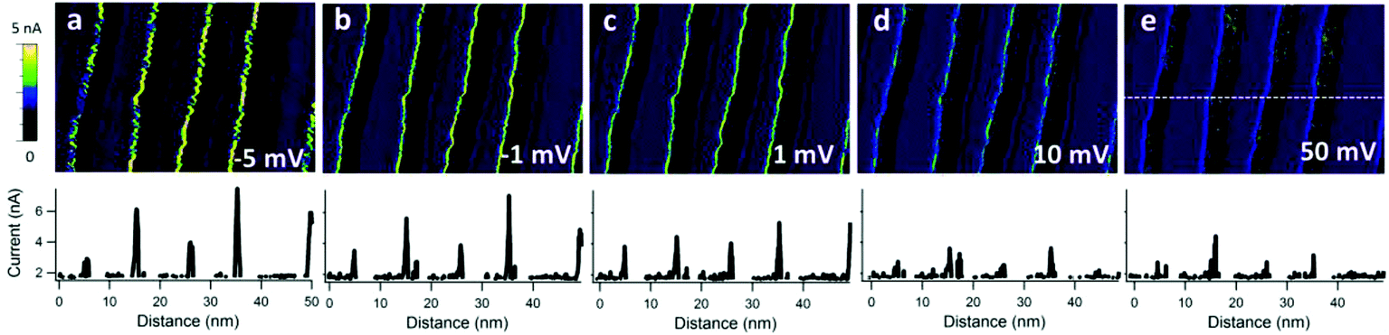 | ||
| Fig. 4 (a)–(e) Current error images of a region of GNR obtained at different bias (see the value in the lower part of the image) together with profiles obtained on the line marked in (e). All the 49 × 32 nm2 images where obtained using a 2 nA setpoint. Intrinsic doping of the graphene by the metal substrate shifts the Fermi level to −7 mV. Close to the Fermi level the charge carriers can tunnel resonantly and the conductivity is enhanced. As the bias is increased and diverges from the Fermi level, the electrons cannot tunnel elastically to the edge state, decreasing the conductivity. | ||
Theory predicts that narrow graphene nanoribbons present antiferromagnetic (AFM) coupling between facing edges, which results in the opening of a bandgap between the states of opposite polarization.6,7,12,13,38 Here, we propose that the covalent bonds between Pt and C atoms of the border-like edge quench the associated graphene edge state preventing any bandgap opening and inducing the observed metallic behavior. In addition, we expect the step-like associated edge state to keep its magnetization and to be spin-polarized as the edge state is localized in only one of the sublattices.39–41 To explore the spin magnetization of one isolated edge state in graphene we have performed first principles spin-polarized calculations of wide graphene nanoribbons (see the ESI† for details). Contrary to narrow GNR, the spin-polarized calculations of the particular (3,1) nanoribbon with 10 nm of width show two possible magnetic convergent spin configurations with about the same total energy. Ferromagnetic (FM) and antiferromagnetic (AFM) solutions with parallel and antiparallel net spin-magnetization between edges, respectively, are almost equally stable, indicating that the edge states are magnetically decoupled.
In Fig. 4a, we can observe that the edge state presents wiggles and discontinuities along the edge direction. These faults can result in nm-extended regions of edge state absence (see, for example, the left stripe edge in Fig. 2). The origin of these heterogeneities is still not fully clear to us but it can be related to the edges containing larger amounts of armchair and amorphous regions. The orientation between (√7 × √7)R19° and the direction of the Pt steps forces the observed average (3,1) chirality of the graphene edges which presents the localized edge state. But this relative angle between the substrate and graphene orientation can be locally altered as a result of multiple factors, such as local substrate defects30 or gradients in residual hydrogen concentration.9 The local-scale armchair regions of the atomic configuration at the edge might be responsible for the modulation of the magnitude of the edge states observed in our measurements.
Our graphene growth methodology is very simple and can result in wide (here 10 nm) stripes of hundreds of nanometers length. One may speculate that the use of different vicinal surfaces will yield graphene stripes of tunable widths, hence providing an alternative production method of GNRs and stripes. The edge states obtained under our approach are very robust and stable at room temperature, giving new hopes for the use of the magnetoelectronic and spintronic properties of carbon-based nanomaterials under ambient conditions. Further investigations with spin polarized STM will be of interest.
Conclusions
In conclusion, we have presented an atomic scale study of the metallic edges states appearing at the borders of graphene stripes. We have developed a growth methodology based on the decomposition of C60 molecules on vicinal Pt(111) surfaces which results in large graphene stripes with an average width of 10 nm and hundreds of nanometer long. These graphene one-dimensional structures present one of their edges in a step-like zigzag average configuration, exhibiting high crystallinity and strong edge electronic phenomena. We have performed STM pseudo-constant height current error maps and made use of them to find regions of enhanced conductance on the surface at the edges of the stripes. Confronting our atomic-scale STM images with tight-binding and ab initio DFT calculations, we have identified the edge states spectrally localized around the Fermi level. Measurements of the intensity of the edge states for varying bias voltages further confirm their metallicity and show the robustness of the edge state even at room temperature. The spatial characterization of the electronic states reveals atomic sublattice localization suggesting, in combination with calculations, a non-zero spin polarization and the development of a net magnetic moment.Methods
Experiments
The experiments were performed in a UHV chamber with base pressure 1 × 10⁻¹⁰ mbar. The Pt(111) single crystal was cleaned by conventional repeated cycles of Ar+ sputtering and annealing at 1200 K. The first annealing was performed in an oxygen atmosphere for carbide impurity removal. Graphene was grown after the thermal evaporation of C60 for 40 min at a rate of 0.4 monolayer per hour onto the sample held at RT and subsequent annealing at 1200 K for 10 min. Regions of step bunched surfaces were found coexisting with the zones of extended G/Pt(111) terraces. STM images were acquired by means of a room temperature microscope using both topographic and current error maps in a quasi-constant height mode (as mentioned above) with typical bias between 400 meV and −400 meV and current setpoints up to 4 nA. The thermal drift was corrected in Fig. 3 with a homemade program which resized the images for a given hexagonal unit cell keeping the fast scan axis as the reference distance.Theory
We have employed two types of theoretical calculations to characterize our system. To simulate the properties of semi-infinite systems, we have used a tight-binding approach and the Surface Green Function Matching Method (SFGM); to elucidate the spin polarization of the isolated edge state we have performed ab initio calculations. We describe below each method in more detail.Tight-binding approach plus SFGM method
We model semi-infinite edges using a π-orbital tight-binding Hamiltonian, H0 with the nearest neighbor hopping parameter, t = −2.66 eV. This model has been shown to give the electronic properties of graphene and carbon nanotube nanostructures in good agreement with ab initio calculations.6,42,43 We study semi-infinite periodical edges, so a wavevector parallel to the edge can be defined. In the direction perpendicular to the edge, there is no translational symmetry; therefore, the Green function is recursively calculated as a function of the edge wavevector. From the “surface” (edge) Green function, the local density of states can be evaluated. More details can be found in ref. 44.Ab initio calculations
The electronic and magnetic properties of GNRs have been obtained employing ab initio spin-polarized calculations with the SIESTA code.45 We use GGA calculations with a revPBE functional. The electron-ion interactions are modeled with norm-conserving nonlocal Troullier–Martins pseudopotentials generated with the atomic configuration [He]2s22p2 taken as reference described with a double ζ singly polarized basis set. The energy cutoff is set to 400 Ry. The structures were relaxed by conjugate gradient optimization until the forces were smaller than 0.01 eV Å−1. Periodic boundary conditions were applied along the one-dimensional long axis of the ribbon, so we use sufficiently large supercell parameters (15 Å) in the perpendicular directions to avoid spurious interactions between adjacent ribbons. All carbon atoms at the edges are passivated by hydrogen.Acknowledgements
P. M. was supported by the “Rafael Calvo Rodés” Program. L. C. thanks the support of the Spanish MINECO through project FIS2015-64654-P. J. A. M.-G. acknowledges funding from the Spanish MINECO (Grant MAT2014-54231-C4-1-P) and the ERC-Synergy Program (Grant ERC-2013-SYG-610256 Nanocosmos). The research leading to these results has received funding from the European Union Seventh Framework Programme under Grant agreement No. 604391 Graphene Flagship. Open Access funding provided by the Max Planck Society.Notes and references
- X. Zhang, J. Xin and F. Ding, Nanoscale, 2013, 5, 2556–2569 RSC.
- X. Jia, J. Campos-Delgado, M. Terrones, V. Meunier and M. S. Dresselhaus, Nanoscale, 2011, 3, 86–95 RSC.
- J. Cai, C. A. Pignedoli, L. Talirz, P. Ruffieux, H. Söde, L. Liang, V. Meunier, R. Berger, R. Li and X. Feng, Nat. Nanotechnol., 2014, 9, 896–900 CrossRef CAS PubMed.
- Y.-C. Chen, T. Cao, C. Chen, Z. Pedramrazi, D. Haberer, D. G. de Oteyza, F. R. Fischer, S. G. Louie and M. F. Crommie, Nat. Nanotechnol., 2015, 10, 156–160 CrossRef CAS PubMed.
- J. Cai, P. Ruffieux, R. Jaafar, M. Bieri, T. Braun, S. Blankenburg, M. Muoth, A. P. Seitsonen, M. Saleh and X. Feng, Nature, 2010, 466, 470–473 CrossRef CAS PubMed.
- W. Jaskólski, A. Ayuela, M. Pelc, H. Santos and L. Chico, Phys. Rev. B: Condens. Matter, 2011, 83, 235424 CrossRef.
- Y.-W. Son, M. L. Cohen and S. G. Louie, Phys. Rev. Lett., 2006, 97, 216803 CrossRef PubMed.
- S. Kawai, A. Benassi, E. Gnecco, H. Söde, R. Pawlak, X. Feng, K. Müllen, D. Passerone, C. A. Pignedoli and P. Ruffieux, Science, 2016, 351, 957–961 CrossRef CAS PubMed.
- T. Wassmann, A. P. Seitsonen, A. M. Saitta, M. Lazzeri and F. Mauri, Phys. Rev. Lett., 2008, 101, 096402 CrossRef PubMed.
- X. Zhang, O. V. Yazyev, J. Feng, L. Xie, C. Tao, Y.-C. Chen, L. Jiao, Z. Pedramrazi, A. Zettl and S. G. Louie, ACS Nano, 2012, 7, 198–202 CrossRef PubMed.
- P. Han, K. Akagi, F. Federici Canova, R. Shimizu, H. Oguchi, S. Shiraki, P. S. Weiss, N. Asao and T. Hitosugi, ACS Nano, 2015, 9, 12035–12044 CrossRef CAS PubMed.
- K. Nakada, M. Fujita, G. Dresselhaus and M. S. Dresselhaus, Phys. Rev. B: Condens. Matter, 1996, 54, 17954 CrossRef CAS.
- O. V. Yazyev and M. Katsnelson, Phys. Rev. Lett., 2008, 100, 047209 CrossRef PubMed.
- O. V. Yazyev, Rep. Prog. Phys., 2010, 73, 056501 CrossRef.
- X. Jia, M. Hofmann, V. Meunier, B. G. Sumpter, J. Campos-Delgado, J. M. Romo-Herrera, H. Son, Y.-P. Hsieh, A. Reina and J. Kong, Science, 2009, 323, 1701–1705 CrossRef CAS PubMed.
- M. Fujihara, R. Inoue, R. Kurita, T. Taniuchi, Y. Motoyui, S. Shin, F. Komori, Y. Maniwa, H. Shinohara and Y. Miyata, ACS Nano, 2015, 9, 9027–9033 CrossRef CAS PubMed.
- S. Berciaud, S. Ryu, L. E. Brus and T. F. Heinz, Nano Lett., 2008, 9, 346–352 CrossRef PubMed.
- W. A. De Heer, C. Berger, X. Wu, P. N. First, E. H. Conrad, X. Li, T. Li, M. Sprinkle, J. Hass and M. L. Sadowski, Solid State Commun., 2007, 143, 92–100 CrossRef CAS.
- C. Berger, Z. Song, X. Li, X. Wu, N. Brown, C. Naud, D. Mayou, T. Li, J. Hass, A. N. Marchenkov, E. H. Conrad, P. N. First and W. A. de Heer, Science, 2006, 312, 1191–1196 CrossRef CAS PubMed.
- G. Z. Magda, X. Jin, I. Hagymási, P. Vancsó, Z. Osváth, P. Nemes-Incze, C. Hwang, L. P. Biró and L. Tapasztó, Nature, 2014, 514, 608–611 CrossRef CAS PubMed.
- D. V. Kosynkin, A. L. Higginbotham, A. Sinitskii, J. R. Lomeda, A. Dimiev, B. K. Price and J. M. Tour, Nature, 2009, 458, 872–876 CrossRef CAS PubMed.
- C. Tao, L. Jiao, O. V. Yazyev, Y.-C. Chen, J. Feng, X. Zhang, R. B. Capaz, J. M. Tour, A. Zettl and S. G. Louie, Nat. Phys., 2011, 7, 616–620 CrossRef CAS.
- L. Talirz, P. Ruffieux and R. Fasel, Adv. Mater., 2016, 6222–6231 CrossRef CAS PubMed.
- P. Ruffieux, S. Wang, B. Yang, C. Sanchez, J. Liu, T. Dienel, L. Talirz, P. Shinde, C. A. Pignedoli and D. Passerone, Nature, 2016, 531, 489–492 CrossRef CAS PubMed.
- A. Kimouche, M. M. Ervasti, R. Drost, S. Halonen, A. Harju, P. M. Joensuu, J. Sainio and P. Liljeroth, Nat. Commun., 2015, 6 CAS , 10177.
- S. Wang, L. Talirz, C. A. Pignedoli, X. Feng, K. Mullen, R. Fasel and P. Ruffieux, Nat. Commun., 2016, 7 Search PubMed , 11507.
- E. Hahn, H. Schief, V. Marsico, A. Fricke and K. Kern, Phys. Rev. Lett., 1994, 72, 3378 CrossRef CAS PubMed.
- M. Yoon, S. Mochrie, D. Zehner, G. Watson and D. Gibbs, Surf. Sci., 1995, 338, 225–235 CrossRef CAS.
- P. Gambardella, M. Blanc, H. Brune, K. Kuhnke and K. Kern, Phys. Rev. B: Condens. Matter, 2000, 61, 2254 CrossRef CAS.
- G. Otero, C. Gonzalez, A. L. Pinardi, P. Merino, S. Gardonio, S. Lizzit, M. Blanco-Rey, K. Van de Ruit, C. Flipse and J. Méndez, Phys. Rev. Lett., 2010, 105, 216102 CrossRef CAS PubMed.
- P. Merino, M. Švec, A. L. Pinardi, G. Otero and J. A. Martín-Gago, ACS Nano, 2011, 5, 5627–5634 CrossRef CAS PubMed.
- J. I. Martínez, P. Merino, A. L. Pinardi, O.-I. Gonzalo, M. F. López, J. Méndez and J. A. Martín-Gago, Sci. Rep., 2016, 6 Search PubMed , 20354.
- J. Coraux, A. T. N'Diaye, C. Busse and T. Michely, Nano Lett., 2008, 8, 565–570 CrossRef CAS PubMed.
- S. Marchini, S. Günther and J. Wintterlin, Phys. Rev. B: Condens. Matter, 2007, 76, 075429 CrossRef.
- S.-H. Phark, J. Borme, A. L. Vanegas, M. Corbetta, D. Sander and J. Kirschner, Phys. Rev. B: Condens. Matter, 2012, 86, 045442 CrossRef.
- P. Merino, L. Rodrigo, A. L. Pinardi, J. Méndez, M. F. López, P. Pou, R. Pérez and J. A. Martín Gago, ACS Nano, 2014, 8, 3590–3596 CrossRef CAS PubMed.
- M. Ondráček, P. Pou, V. Rozsíval, C. González, P. Jelínek and R. Pérez, Phys. Rev. Lett., 2011, 106, 176101 CrossRef PubMed.
- H. Santos, A. Ayuela, L. Chico and E. Artacho, Phys. Rev. B: Condens. Matter, 2012, 85, 245430 CrossRef.
- H. Santos, D. Soriano and J. J. Palacios, Phys. Rev. B: Condens. Matter, 2014, 89, 195416 CrossRef.
- A. Rycerz, J. Tworzydło and C. Beenakker, Nat. Phys., 2007, 3, 172–175 CrossRef CAS.
- H. González-Herrero, J. M. Gómez-Rodríguez, P. Mallet, M. Moaied, J. J. Palacios, C. Salgado, M. M. Ugeda, J.-Y. Veuillen, F. Yndurain and I. Brihuega, Science, 2016, 352, 437–441 CrossRef PubMed.
- A. Ayuela, L. Chico and W. Jaskólski, Phys. Rev. B: Condens. Matter, 2008, 77, 085435 CrossRef.
- O.-A. Dobrescu and M. Apostol, Can. J. Phys., 2015, 93, 580–584 CrossRef CAS.
- L. Chico, L. X. Benedict, S. G. Louie and M. L. Cohen, Phys. Rev. B: Condens. Matter, 1996, 54, 2600–2606 CrossRef CAS.
- M. S. José, A. Emilio, D. G. Julian, G. Alberto, J. Javier, O. Pablo and S.-P. Daniel, J. Phys.: Condens. Matter, 2002, 14, 2745 CrossRef.
Footnotes |
| † Electronic supplementary information (ESI) available. See DOI: 10.1039/c7nr00367f |
| ‡ Present address: Max Planck Institute for Solid State Research, Heisenbergstrasse 1, D-70569, Stuttgart, Germany. |
| This journal is © The Royal Society of Chemistry 2017 |