
 Open Access Article
 This Open Access Article is licensed under a
 Creative Commons Attribution 3.0 Unported Licence
Large-area tungsten disulfide for ultrafast photonics
Peiguang
Yan
 *a,
Hao
Chen
a,
Jinde
Yin
a,
Zihan
Xu
b,
Jiarong
Li
a,
Zike
Jiang
a,
Wenfei
Zhang
a,
Jinzhang
Wang
a,
Irene Ling
Li
a,
Zhipei
Sun
c and
Shuangchen
Ruan
*a
*a,
Hao
Chen
a,
Jinde
Yin
a,
Zihan
Xu
b,
Jiarong
Li
a,
Zike
Jiang
a,
Wenfei
Zhang
a,
Jinzhang
Wang
a,
Irene Ling
Li
a,
Zhipei
Sun
c and
Shuangchen
Ruan
*a
aShenzhen Key Laboratory of Laser Engineering, College of Optoelectronic Engineering, Shenzhen University, Nanhai Avenue 3688, Shenzhen 518060, China. E-mail: yanpg@szu.edu.cn; scruan@szu.edu.cn
bShenzhen 6Carbon Technology, China
cDepartment of Micro- and Nanosciences, Aalto University, Tietotie 3, FI-02150 Espoo, Finland
First published on 29th December 2016
Abstract
Two-dimensional (2D) layered transition metal dichalcogenides (TMDs) have attracted significant interest in various optoelectronic applications due to their excellent nonlinear optical properties. One of the most important applications of TMDs is to be employed as an extraordinary optical modulation material (e.g., the saturable absorber (SA)) in ultrafast photonics. The main challenge arises while embedding TMDs into fiber laser systems to generate ultrafast pulse trains and thus constraints their practical applications. Herein, few-layered WS2 with a large-area was directly transferred on the facet of the pigtail and acted as a SA for erbium-doped fiber laser (EDFL) systems. In our study, WS2 SA exhibited remarkable nonlinear optical properties (e.g., modulation depth of 15.1% and saturable intensity of 157.6 MW cm−2) and was used for ultrafast pulse generation. The soliton pulses with remarkable performances (e.g., ultrashort pulse duration of 1.49 ps, high stability of 71.8 dB, and large pulse average output power of 62.5 mW) could be obtained in a telecommunication band. To the best of our knowledge, the average output power of the mode-locked pulse trains is the highest by employing TMD materials in fiber laser systems. These results indicate that atomically large-area WS2 could be used as excellent optical modulation materials in ultrafast photonics.
1. Introduction
Recently, transition metal dichalcogenides (TMDs) have attracted significant attention due to their scientific interest and technological significance.1–6 Depending on the intrinsic properties of TMDs, they could be catalogued as metallic materials (e.g., niobium disulfide (NbS2) and tantalum disulfide (TaS2)), semiconducting materials (e.g., tungsten disulfide (WS2), tungsten diselenide (WSe2), molybdenum disulfide (MoS2), and molybdenum diselenide (MoSe2)), and insulating materials (e.g., hafnium disulfide (HfS2)).7–9 Compared with metallic or insulating counterparts, semiconducting TMDs have gained extensive attention due to their tunable bandgap with variable thicknesses, which leads to unique layer-dependent optoelectronic properties. For instance, the bandgap of WS2 has a transition from the indirect bandgap in the bulk form to the direct bandgap in the monolayer.8 This tunable-bandgap property of semiconducting TMDs has opened up new opportunities for optoelectronic applications, such as a flexible approach to engineer their optical properties by changing the thickness.As a representative of the semiconducting TMD family, WS2 has unique properties such as high carrier dynamics (∼140 cm2 V−1 s−1), high third-order nonlinear susceptibility (Im![[thin space (1/6-em)]](https://www.rsc.org/images/entities/char_2009.gif) χ3 ∼ 10−8), and broadband light absorption.10–12 Moreover, the theoretical models predict that WS2 has the highest carrier mobility among the semiconducting TMDs due to a better ballistic performance.13 One of the most important applications for WS2 based on the abovementioned properties is to employ few-layer WS2 as an excellent optical modulation material for pulsed lasers, which is an elementary component to modulate the laser continuous wave output into a train of optical pulse via intensity-dependent transmission property. By employing passive Q-switching or mode-locking techniques, various researchers have generated stable pulse trains in fiber laser systems utilizing few-layer WS2 as a remarkable SA. For example, passive Q-switching operation with great performances could be achieved at different central wavelengths (e.g. 635 nm, 1030 nm, 1560 nm, and 1925 nm) and ultrashort pulses (ranging from a few picoseconds to hundreds of femtoseconds) could be generated in fiber laser systems.14–17 However, as for SAs based on few-layer WS2, some shortcomings exist that have yet to be overcome and these constraint their practical applications. For instance, most of previous reports on pulsed laser studies employed a liquid exfoliation (LPE) method or mechanical exfoliation (ME) method to prepare few-layer WS2. Conventionally, few-layer WS2 was obtained via LPE or ME methods resulting in an uncontrollable size and random thickness, which limits the performances of WS2 once employed in a fiber laser system. Furthermore, these disadvantages result in a more complicated process to prepare saturable absorbers based on few-layer WS2. For example, few-layer WS2 prepared by the two abovementioned methods has to be mixed with a host polymer (such as polyvinyl alcohol (PVA), or cellulose derivatives (NaCMC)) to form free-standing composites.16,18 The development of few-layered WS2 with greater performances, such as large areas, uniform thicknesses, and high crystallinity, are imminently demanded to overcome the limitations of the abovementioned methods. Recently, enormous progress on the growth of WS2 by a chemical vapour deposition (CVD) method has significantly decreased the complexity to prepare few-layered WS2 with a large-area and offered a more efficient approach to study the optoelectronic properties of WS2.20–23 Recent reports of the SAs based on atomic-layer WS2 exhibited the potential of this 2D semiconducting material and passive mode locking operation could be achieved, incorporated with few-layered WS2 nanosheets.24 However, the saturable absorption mechanism of few-layered WS2 with a large-area has not yet been demonstrated and understood. Moreover, the literature contains few reports on the investigations of nonlinear optical properties of few-layered WS2 with a large-area and its applications in ultrafast photonics. Therefore, it is desirable that more experiments of few-layered WS2 to characterize its nonlinear optical properties and applications in ultrafast pulsed fiber lasers should be explored and studied, which are essential for practical applications.
χ3 ∼ 10−8), and broadband light absorption.10–12 Moreover, the theoretical models predict that WS2 has the highest carrier mobility among the semiconducting TMDs due to a better ballistic performance.13 One of the most important applications for WS2 based on the abovementioned properties is to employ few-layer WS2 as an excellent optical modulation material for pulsed lasers, which is an elementary component to modulate the laser continuous wave output into a train of optical pulse via intensity-dependent transmission property. By employing passive Q-switching or mode-locking techniques, various researchers have generated stable pulse trains in fiber laser systems utilizing few-layer WS2 as a remarkable SA. For example, passive Q-switching operation with great performances could be achieved at different central wavelengths (e.g. 635 nm, 1030 nm, 1560 nm, and 1925 nm) and ultrashort pulses (ranging from a few picoseconds to hundreds of femtoseconds) could be generated in fiber laser systems.14–17 However, as for SAs based on few-layer WS2, some shortcomings exist that have yet to be overcome and these constraint their practical applications. For instance, most of previous reports on pulsed laser studies employed a liquid exfoliation (LPE) method or mechanical exfoliation (ME) method to prepare few-layer WS2. Conventionally, few-layer WS2 was obtained via LPE or ME methods resulting in an uncontrollable size and random thickness, which limits the performances of WS2 once employed in a fiber laser system. Furthermore, these disadvantages result in a more complicated process to prepare saturable absorbers based on few-layer WS2. For example, few-layer WS2 prepared by the two abovementioned methods has to be mixed with a host polymer (such as polyvinyl alcohol (PVA), or cellulose derivatives (NaCMC)) to form free-standing composites.16,18 The development of few-layered WS2 with greater performances, such as large areas, uniform thicknesses, and high crystallinity, are imminently demanded to overcome the limitations of the abovementioned methods. Recently, enormous progress on the growth of WS2 by a chemical vapour deposition (CVD) method has significantly decreased the complexity to prepare few-layered WS2 with a large-area and offered a more efficient approach to study the optoelectronic properties of WS2.20–23 Recent reports of the SAs based on atomic-layer WS2 exhibited the potential of this 2D semiconducting material and passive mode locking operation could be achieved, incorporated with few-layered WS2 nanosheets.24 However, the saturable absorption mechanism of few-layered WS2 with a large-area has not yet been demonstrated and understood. Moreover, the literature contains few reports on the investigations of nonlinear optical properties of few-layered WS2 with a large-area and its applications in ultrafast photonics. Therefore, it is desirable that more experiments of few-layered WS2 to characterize its nonlinear optical properties and applications in ultrafast pulsed fiber lasers should be explored and studied, which are essential for practical applications.
In this report, we have grown uniform few-layered WS2 (up to 4 layers) at the centimeter-scale by a CVD process. By a transfer process, few-layered WS2 was directly transferred on the facet of the pigtail and embedded into an EDFL system with a typical ring cavity structure. We investigated the nonlinear optical properties of few-layered WS2 with large areas. Herein, WS2 SA exhibited excellent nonlinear optical performances, such as a large modulation depth (MD of 15.1%) and lower saturable intensity (157.6 MW cm−2), which are beneficial to achieve passive mode-locking operation in fiber laser systems. In our experiment that used a few-layered WS2 SA, the soliton mode-locked pulses could be attained in an EDFL system with excellent laser performances such as a pulse duration of 1.49 ps, signal to noise ratio (SNR) of 71.8 dB, and an average output pulse power of 62.5 mW, showing its feasibility for use in ultrafast pulsed fiber lasers.
2. Experimental section
2.1. Synthesis and characterization of large-area few-layer WS2
Fig. 1(a) schematically illustrates the CVD process of the grown large-area WS2 few layers on the sapphire substrates. Briefly, tungsten oxide (WO3) powder was used as a precursor for tungsten. The WO3 powder positioned on a silicon substrate placed in the centre of the furnace and close to the sapphire substrates was used as growth substrates. Then, the sulfur powder was placed beside WO3. Employing a slow heating rate of 15 °C min−1, the reaction temperature of chamber was increased to 1000 °C min−1. While keeping this temperature for 30 min, sulfur was evaporated and reacted with WO3. After this, the heater of the furnace was turned off, and the sample was left in the chamber to cool down to room temperature.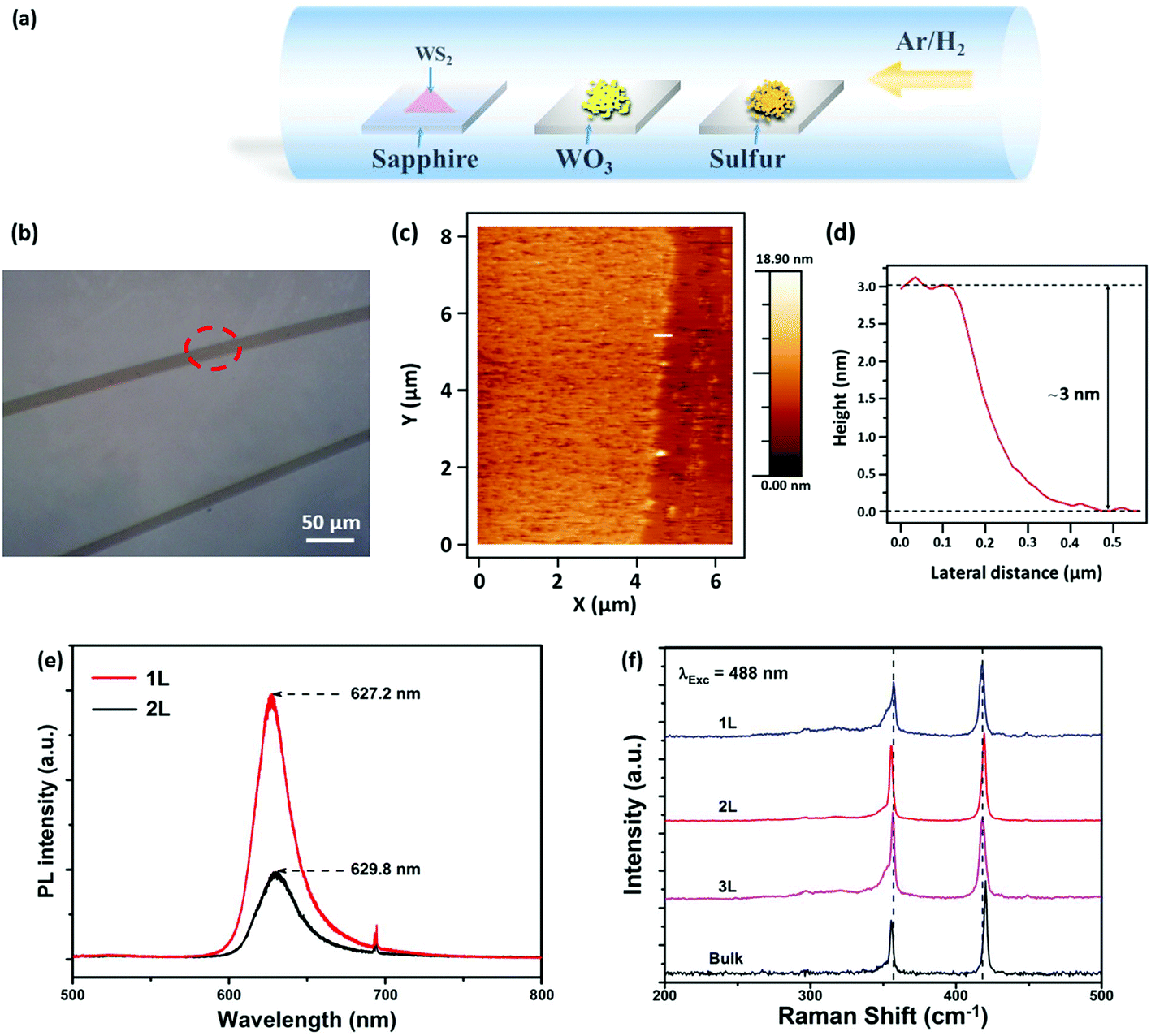 | ||
| Fig. 1 (a) Schematic of the growth of few-layer WS2 by a CVD method. (b) Optical microscopy image of few-layer WS2 with a large-area grown on sapphire substrate. (c) The AFM image of WS2 corresponding to the position of the red circle in (b). (d) Height profile (along the white line in (c)). (e) PL spectra excited at 488 nm for the WS2 with a monolayer (1L) and bilayer (2L). (f) Raman spectra with different WS2 thicknesses (such as 1L, 2L, 3L, and bulk form). | ||
The morphologies of the large-area WS2 are presented in Fig. 1(b) by an optical image, where uniform few-layer WS2 with a large-area could be distinctly observed. To identify the number of layers of the WS2 film on the sapphire substrate, atomic force microscopy (AFM) was used to determine the thickness of the WS2 film, as shown in Fig. 1(c). Fig. 1(d) is the height profile, from which a height of ∼3 nm could be extracted. However, a thickness of ∼0.7 nm of the monolayer WS2 was identified in the previous reports by mechanical exfoliation method; WS2 film in the present system corresponds to four layers.10 The photoluminescence (PL) spectra of the monolayer (1L) and bilayer (2L) were excited by 488 nm laser and are shown in Fig. 1(e). The PL intensity is observed to be significantly thickness-dependent.25 The monolayer PL intensity of WS2 is enhanced by orders of magnitude compared with bilayer. As for monolayer WS2 prepared in our experiment, a strong emission is exhibited at 627.2 nm, corresponding to the direct excitonic transition at the κ point.20 However, the emission wavelength of bilayer is slightly red-shifted to 629.8 nm, which is consistent with the thickness-dependent bandgap property of WS2 caused by stronger out-of-plane quantum confinement with the decreasing thickness. Fig. 1(f) is the Raman spectra of WS2 excited by 488 nm laser with different thickness (monolayer, bilayer, triple-layer, and bulk). There are two Raman characteristic peaks of WS2 in the Raman spectra, assigned to two photon modes (E2g1 and A1g).20 Note that the absolute intensity of all Raman modes was increased with the number of layers, which is consistent with a previous report that the Raman intensity of WS2 is mainly affected by the scattering volume.26
3. Few-layered WS2-based saturable absorber
3.1. Preparation process of the WS2-based SA
Fig. 2(a) schematically exhibits the preparation process of saturable absorbers based on the few-layered WS2 with a large area. Briefly, after growing few-layered WS2 on the sapphire substrate, the WS2 film was coated by a thin film of polymethylmethacrylate (PMMA). Then, the WS2-PMMA composite was stripped from the sapphire substrate and transferred to deionized (DI) water to remove the residues. After this, the PMMA-supported WS2 film was transferred to acetone to sufficiently remove PMMA. The free-standing WS2 film was transferred to DI water and suspended on its surface. Finally, the WS2 film was transferred on the facet of the pigtail. While DI water is volatile at room temperature, the WS2 film was closely combined on the facet of the pigtail by a van der Waals force. Note that in our experiment, large-area WS2 films were transferred on both sides of the pigtails to increase the effect of nonlinear optical properties and obtain a more stable generation of pulses.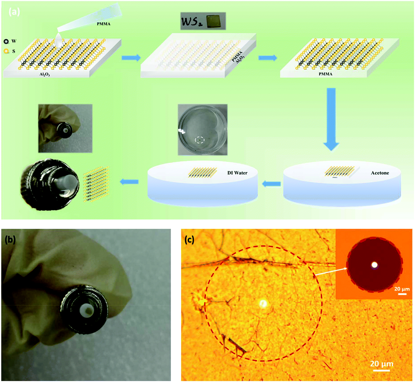 | ||
| Fig. 2 (a) Schematic of the saturable absorbers prepared by transferring few-layer WS2 on the facet of the fiber pigtail. (b) and (c) image and microscope image of the facet for the fiber pigtail coated with large-area WS2 films. The inset in (c) is the optical microscopic image for the pigtail with a clear facet. | ||
3.2. Nonlinear optical properties of WS2-based SA
The nonlinear optical absorption properties of the saturable absorber based on the few-layered WS2 was measured by a balanced twin-detector method, as shown in Fig. 3(a).27 The homemade mode-locked fiber laser was operated at a central wavelength of 1562 nm with a 921 fs pulse duration and fundamental frequency of 17.04 MHz. The nonlinear saturable absorption curve of our WS2 SA is shown in Fig. 3(b). In our experiment, the MD of our WS2 SA was 15.1% and the saturable intensity was 157.6 MW cm−2. According to the two-level model (eqn (1)) for the interpretation of the saturable absorption property of TMDs, where αsat is the modulation depth (MD), αnon-sat is the non-saturable loss, and Isat is the saturable intensity, the value of MD for our WS2 SA might be larger than the measured value, which is limited by the measured range of our equipment.28–30 The large value for MD of WS2 SA was beneficial to achieve stable passive mode locking operation with an ultra-short pulse duration. The nonsaturable loss was comparable to other 2D material-based SAs (such as graphene, MoS2, or WS2) prepared by a liquid phase exfoliation method.31–35 Due to our WS2 SA, prepared without any organic host polymer material, the insertion loss of SA in the fiber laser cavity obviously decreased. Note that in our experiments, the few-layer WS2 exhibited nonlinear saturable absorption at NIR wavelengths (i.e., 1562 nm, corresponding to 0.79 eV) with sub-bandgap photon energies, which are below the WS2 material bandgap photon energy (e.g., 2.1 eV for the monolayer and 1.3 eV for the bulk form). It is understood that larger-area WS2 few layers are stacked by a monolayer with triangular shapes because the growth is not self-limiting, leading to abundant edge-state saturable absorption caused by the boundaries of a finite crystal structure.34,35 Recently, a great deal of research has also been reported for sub-bandgap saturable absorption of TMDs.14–19 | (1) |
 | ||
| Fig. 3 (a) Schematic of the balanced twin-detector equipment for the measurement of nonlinear transmission of SA based on few-layer WS2. Variable optical attenuator (VOA) and output coupler (OC). (b) Nonlinear absorption curve of few-layer WS2. (c) The configuration of passively mode-locked fiber laser based on few-layer WS2 SA. | ||
4. Results and discussion
An EDFL system with a typical ring cavity configuration was employed in our experiment to verify the nonlinear optical properties of atomic-layer WS2. The schematic of the fiber laser is shown in Fig. 3(c). A wavelength division multiplex (WDM) was used to inject the pump power into the cavity. A 1.5 m EDF (OFS) was employed to act as gain media. The unidirectional transition of light was ensured by a polarization independent isolator (PI-ISO). Note that in our laser cavity, all components were polarization-independent, which avoided the self-starting mode-locking operation induced by nonlinear polarization evolution (NPE). The optical coupler (OC) with a 30/70 splitting ratio was used to generate extra pulses for the measurement. The polarization controller (PC) was utilized to adjust the polarization state within the laser cavity to optimize the laser performances. Two sections of the single mode fiber (SMF1 and SMF2) were employed to balance the dispersion of the cavity and ensure that the passive mode-locking was operated at the soliton state with anomalous net cavity dispersion. The total cavity length was 424.8 m.The self-starting mode-locking operation was achieved when the pump power was increased to 140 mW. The relationship between the pump power and laser output power is presented in Fig. 4(a). The mode-locking operation was still working while the pump power was adjusted from 140 mW to 440 mW. As shown in Fig. 4(b), when the pump power was set to 440 mW, stable passive mode-locking could be attained with a central wavelength of 1568.3 nm and a 3 dB bandwidth of 1.94 nm. Fig. 4(c) shows the SNR of output pulses of 71.8 dB with a 10 Hz resolution bandwidth (RBW). The repetition rate for the output pulse train was 487 kHz, which is well matched with the cavity roundtrip time, and verifies that the laser was working in the fundamental mode-locking operation. The autocorrelation (AC) trace of the mode-locked pulses with 2.3 ps full half width at half maximum (FWHM) is shown in Fig. 4(d), which was well fitted by as sech2 profile and verified that the mode locked fiber laser operated at the soliton state. After using a 0.648 decorrelation factor for sech2 pulses, the real pulse width was calculated to be 1.49 ps. The time-bandwidth product (TBP) was calculated to be 0.353 and the pulses are near-transform-limited (0.315). The slope efficiency for the mode-locked fiber laser was ∼14%. The maximum output power was measured to be 62.5 mW, corresponding to 128.3 nJ for single pulse energy. To the best of our knowledge, the average output power was the highest by employing TMD materials in fiber laser systems, and we believe that the higher output power could be obtained by further improving the laser cavity design and optimizing the SA properties. The great performances of our few-layered WS2 SA operated at high pump power can be illustrated as follows: (1) the tight combination between large-area WS2 films and the facet of the pigtail could sufficiently reduce the nonsaturable loss, which is of benefit for a lower laser threshold and higher laser slope efficiency, (2) compared with the same WS2 materials prepared by other methods such as LPE and ME, growing few-layer WS2 with a large-area by a CVD process has many advantages such as large areas, uniform thicknesses, and high crystallinity, which results in a faster carrier mobility and is conducive to thermal dissipation of the materials on the facet of pigtails. Unlike using PVA (or NaCMC) to prepare free-standing PVA (or NaCMC)-supporting SA composites, directly coating atomic-layers on the facet of the pigtail could prevent the material properties from being effected by the combination with other organic host polymer materials,36–39 and (3) in our experiment, both sides of the pigtail coated with large-area WS2 films could be of benefit to increase the nonlinear optical properties of the WS2-based SA (such as greater modulation ability and higher damage-resistance) and are conducive to high energy pulse generation. In our experiment, the laser cavity required extra 400 m SMF to compensate the net cavity dispersion into anomalous dispersion. This result is similar to a previous report using monolayer graphene as saturable absorbers.31,40 It is believed that few-layer WS2 also has a high value of normal dispersion. When using a short laser cavity length (typical ∼10 m) without extra SMF, there was no pulse generation and the cavity could only function in continuous-wave (CW) operation. However, after adding an extra SMF with a length of 400 m into the laser cavity, the Kelly sides could be distinctly observed at a low pump power. When the pump power was increased to 440 mW, the Kelly sides were not very obvious in the optical spectrum. However, the output pulses could be well fitted by a sech2 profile, which verifies that the mode locked fiber laser still works in the soliton state. This result is also in agreement with some numerical simulations.41 Since the self-phase modulation (SPM) offers a negative dispersion for passively mode-locked operation, the SPM effect could be stronger at a higher pump power resulting in a lager negative dispersion.
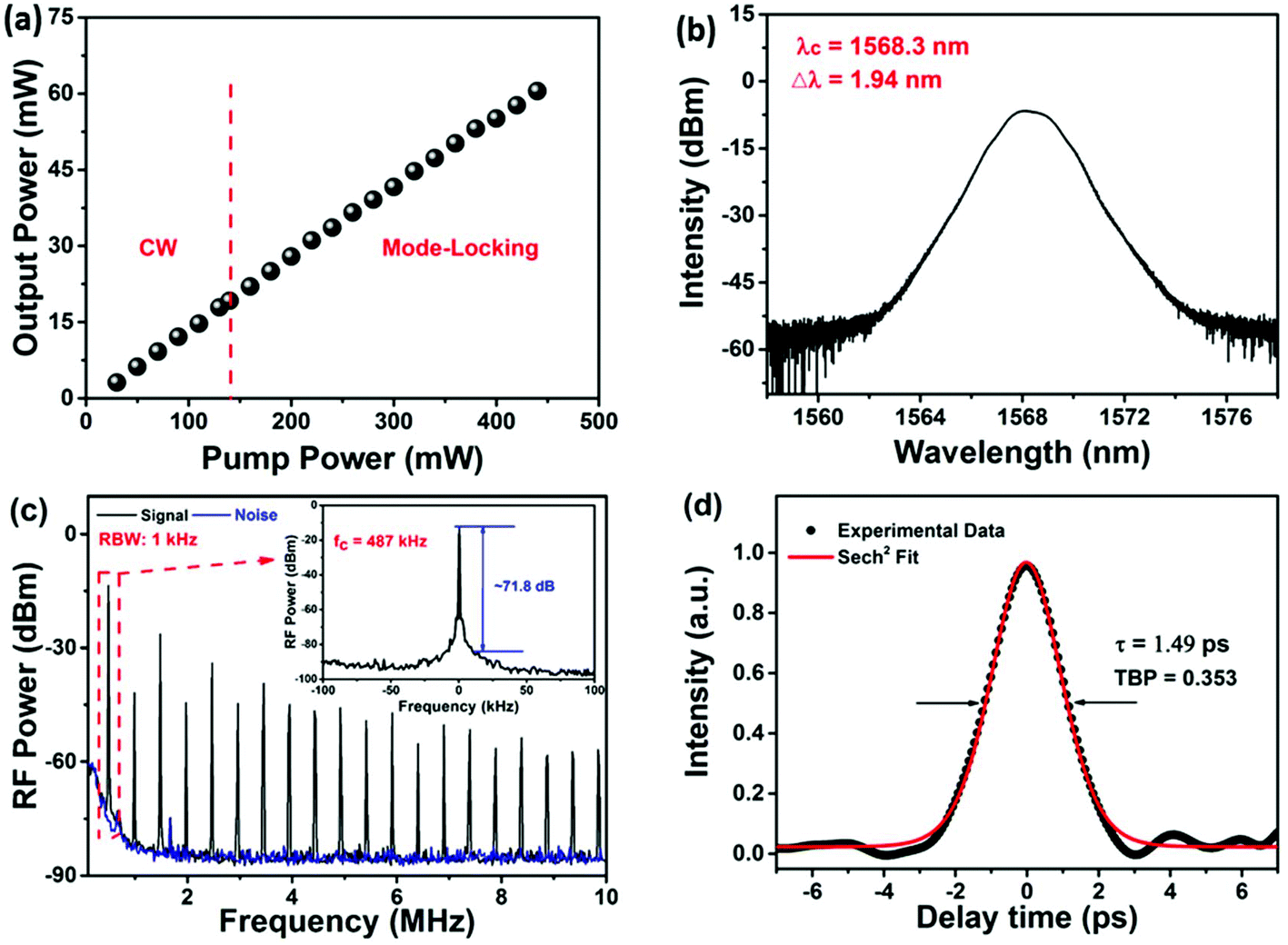 | ||
| Fig. 4 (a) Relationship between the pump power and laser output power. (b) Optical spectrum with the bandwidth of 1.94 nm. (c) Radio frequency (RF) spectrum at the fundamental frequency of 487 kHz with 10 Hz resolution. (d) Autocorrelation trace for the output pulse with a pulse duration of 1.49 ps by a sech2 fit. | ||
5. Conclusion
In summary, we have grown few-layer WS2 with a large-area by a CVD method. To prevent WS2 being affected by organic host polymer materials, large-area WS2 films were directly transferred to the facet of the pigtail to prepare WS2-based SA devices. The nonlinear optical properties of our WS2 SA were investigated by a balanced twin-detector method. Herein, SA exhibited many merits such as a high modulation depth and small saturable intensity, which are of benefit for a passively mode-locking operation in the fiber laser systems. The stable passively mode-locked EDFL operated at the soliton state was obtained by an embedded WS2-based SA. The output pulse trains had an ultrashort pulse duration of 1.49 ps, a SNR of 71.8 dB, and an average output pulse power of 62.5 mW. The results demonstrate that atomically large-area WS2 could be used as an excellent optical modulation material in ultrafast photonics.Acknowledgements
P. G. Yan conceived the original concept and designed the experiments. H. Chen performed the experiments and analyzed the experimental data. J. D. Yin measured the properties of the layered tungsten disulfide. J. R. Li and Z. K. Jiang tested the nonlinear optical properties of the saturable absorbers. Z. H. Xu prepared the saturable absorption materials and discussed the experimental data. The authors thank W. F. Zhang, J. Z. Wang, I. L. Li, and S. C. Ruan for their scientific discussion and considerable improvement in the manuscript presentation. P. G. Yan, H. Chen, and Z. P. Sun co-wrote the manuscript. All authors discussed the results and substantially contributed to the manuscript. This work was supported by the National Natural Science Foundation of China (61605122), the Shenzhen Science and Technology Project (JCYJ 20160427105041864, JSGG 20160429114438287, and JCYJ 20150324140036862), the BUPT (IPOC2015B003), and the Natural Science Foundation of Guangdong Province (2016A030310049).Notes and references
- J. A. Wilson and A. D. Yoffe, Adv. Phys., 1969, 18, 193–335 CrossRef CAS.
- K. Kang, S. Xie, L. Huang, Y. Han, P. Y. Huang, K. F. Mak, C. J. Kim, D. Muller and J. Park, Nature, 2015, 520, 656–660 CrossRef CAS PubMed.
- A. C. Ferrari, F. Bonaccorso, V. Falko, K. S. Novoselov, S. Roche, P. Bøggild, S. Borini, F. Koppens, V. Palermo, N. Pugno, J. A. Garrido, R. Sordan, A. Bianco, L. Ballerini, M. Prato, E. Lidorikis, J. Kivioja, C. Marinelli, T. Ryhänen, A. Morpurgo, J. N. Coleman, V. Nicolosi, L. Colombo, A. Fert, M. Garcia-Hernandez, A. Bachtold, G. F. Schneider, F. Guinea, C. Dekker, M. Barbone, C. Galiotis, A. Grigorenko, G. Konstantatos, A. Kis, M. Katsnelson, C. W. J. Beenakker, L. Vandersypen, A. Loiseau, V. Morandi, D. Neumaier, E. Treossi, V. Pellegrini, M. Polini, A. Tredicucci, G. M. Williams, B. H. Hong, J. H. Ahn, J. M. Kim, H. Zirath, B. J. van Wees, H. van der Zant, L. Occhipinti, A. Di Matteo, I. A. Kinloch, T. Seyller, E. Quesnel, X. Feng, K. Teo, N. Rupesinghe, P. Hakonen, S. R. T. Neil, Q. Tannock, T. Löfwander and J. Kinaret, Nanoscale, 2015, 7, 4598–4810 RSC.
- Y. Liu, N. O. Weiss, X. Duan, H.-C. Cheng, Y. Huang and X. Duan, Nat. Rev. Mater, 2016, 1, 16042 CrossRef.
- Q. H. Wang, K. Kalantar-Zadeh, A. Kis, J. N. Coleman and M. S. Strano, Nat. Nanotechnol., 2012, 7, 699–712 CrossRef CAS PubMed.
- F. Schwierz, R. Granzner and J. Pezoldt, Nanoscale, 2015, 7, 8261–8283 RSC.
- Y. Ding, Y. Wang, J. Ni, L. Shi, S. Shi and W. Tang, Phys. B, 2011, 406, 2254–2260 CrossRef CAS.
- A. L. Elías, N. Perea-López, A. s. Castro-Beltrán, A. Berkdemir, R. Lv, S. Feng, A. D. Long, T. Hayashi, Y. A. Kim and M. Endo, ACS Nano, 2013, 7, 5235–5242 CrossRef PubMed.
- S. H. Chae, Y. Jin, T. S. Kim, D. S. Chung, H. Na, H. Nam, H. Kim, D. J. Perello, H. Y. Jeong, T. H. Ly and Y. H. Lee, ACS Nano, 2016, 10, 1309–1316 CrossRef CAS PubMed.
- D. Ovchinnikov, A. Allain, Y.-S. Huang, D. Dumcenco and A. Kis, ACS Nano, 2014, 8, 8174–8181 CrossRef CAS PubMed.
- S. Zhang, N. Dong, N. McEvoy, M. O'Brien, S. Winters, N. Berner, N. Yim, Y. Li, X. Zhang, Z. Chen, L. Zhang, G. Duesberg and J. Wang, ACS Nano, 2015, 9, 7142 CrossRef CAS PubMed.
- W. Zhao, Z. Ghorannevis, A. K. Kumar, J. R. Pang, M. Toh, X. Zhang, C. Kloc, P. H. Tan and G. Eda, Nanoscale, 2013, 5, 9677 RSC.
- L. Liu, S. B. Kumar, Y. Ouyang and J. Guo, IEEE Trans. Electron Devices, 2011, 58, 3042–3047 CrossRef CAS.
- Z. Luo, D. Wu, B. Xu, H. Xu, Z. Cai, J. Peng, J. Weng, S. Xu, C. Zhu, F. Wang, Z. Sun and H. Zhang, Nanoscale, 2016, 8, 1066–1072 RSC.
- H. Chen, Y. Chen, J. Yin, X. Zhang, T. Guo and P. Yan, Opt. Express, 2016, 24, 16287–16296 CrossRef PubMed.
- M. Zhang, G. Hu, G. Hu, R. C. Howe, L. Chen, Z. Zheng and T. Hasan, Sci. Rep., 2015, 5, 17482 CrossRef CAS PubMed.
- M. Jung, J. Lee, J. Park, J. Koo, Y. M. Jhon and J. H. Lee, Opt. Express, 2015, 23, 19996–20006 CrossRef PubMed.
- T. Hasan, Z. Sun, F. Wang, F. Bonaccorso, P. H. Tan, A. G. Rozhin and A. C. Ferrari, Adv. Mater., 2009, 21, 3874–3899 CrossRef CAS.
- M. Trushin, E. J. R. Kelleher and T. Hasan, 2016, arXiv:1602.06298.
- H. R. Gutierrez, N. Perea-Lopez, A. L. Elias, A. Berkdemir, B. Wang, R. Lv, F. Lopez-Urias, V. H. Crespi, H. Terrones and M. Terrones, Nano. Lett., 2013, 13, 3447–3454 CrossRef CAS PubMed.
- Y. Zhang, T.-R. Chang, B. Zhou, Y.-T. Cui, H. Yan, Z. Liu, F. Schmitt, J. Lee, R. Moore, Y. Chen, H. Lin, H.-T. Jeng, S.-K. Mo, Z. Hussain, A. Bansil and Z.-X. Shen, Nat. Nanotechnol., 2014, 9, 111–115 CrossRef CAS PubMed.
- J. Xiao, Z. Ye, Y. Wang, H. Zhu, Y. Wang and X. Zhang, Light: Sci. Appl., 2015, 4, e366 CrossRef CAS.
- C. Zhang, S. Wang, L. Yang, Y. Liu, T. Xu, Z. Ning, A. Zak, Z. Zhang, R. Tenne and Q. Chen, Appl. Phys. Lett., 2012, 100, 243101 CrossRef.
- R. Khazaeinezhad, S. H. Kassani, J. Hwanseong, P. Kyung Jun, K. Byoung Yoon, Y. Dong-Il and O. Kyunghwan, IEEE Photonics Technol. Lett., 2015, 27, 1581–1584 CrossRef.
- W. Zhao, Z. Ghorannevis, L. Chu, M. Toh, C. Kloc, P.-H. Tan and G. Eda, ACS Nano, 2013, 7, 791 CrossRef CAS PubMed.
- A. Berkdemir, H. R. Gutiérrez, A. R. Botello-Méndez, N. Perea-López, A. L. Elías, C.-I. Chia, B. Wang, V. H. Crespi, F. López-Urías, J.-C. Charlier, H. Terrones and M. Terrones, Sci. Rep., 2013, 3, 1755 Search PubMed.
- J. Du, Q. Wang, G. Jiang, C. Xu, C. Zhao, Y. Xiang, Y. Chen, S. Wen and H. Zhang, Sci. Rep., 2014, 4, 6346 CrossRef CAS PubMed.
- R. Woodward and E. Kelleher, Appl. Sci., 2015, 5, 1440–1456 CrossRef.
- F. Bonaccorso, Z. Sun, T. Hasan and A. C. Ferrari, Nat. Photonics, 2010, 4, 611–622 CrossRef CAS.
- Y. D. Wang, D. Mao, X. T. Gan, L. Han, C. J. Ma, T. L. Xi, Y. Zhang, W. Y. Shang, S. J. Hua and J. L. Zhao, Opt. Express, 2015, 23, 205–210 CrossRef PubMed.
- Q. Bao, H. Zhang, Y. Wang, Z. Ni, Y. Yan, Z. X. Shen, K. P. Loh and D. Y. Tang, Adv. Funct. Mater., 2009, 19, 3077–3083 CrossRef CAS.
- D. Popa, Z. Sun, F. Torrisi, T. Hasan, F. Wang and A. C. Ferrari, Appl. Phys. Lett., 2010, 97, 203106 CrossRef.
- B. H. Chen, X. Y. Zhang, K. Wu, H. Wang, J. Wang and J. P. Chen, Opt. Express, 2015, 23, 26723–26737 CrossRef PubMed.
- M. Zhang, E. J. R. Kelleher, F. Torrisi, Z. Sun, T. Hasan, D. Popa, F. Wang, A. C. Ferrari, S. V. Popov and J. R. Taylor, Opt. Express, 2012, 20, 25077–25084 CrossRef CAS PubMed.
- K. Wu, X. Y. Zhang, J. Wang, X. Li and J. P. Chen, Opt. Express, 2015, 23, 11453–11461 CrossRef PubMed.
- H. Zhang, S. B. Lu, J. Zheng, J. Du, S. C. Wen, D. Y. Tang and K. P. Loh, Opt. Express, 2014, 22, 7249–7260 CrossRef CAS PubMed.
- D. Mao, Y. Wang, C. Ma, L. Han, B. Jiang, X. Gan, S. Hua, W. Zhang, T. Mei and J. Zhao, Sci. Rep., 2015, 5, 7965 CrossRef CAS PubMed.
- D. Mao, B. Du, D. Yang, S. Zhang, Y. Wang, W. Zhang, X. She, H. Cheng, H. Zeng and J. Zhao, Small, 2016, 12, 1489–1497 CrossRef CAS PubMed.
- R. I. Woodward, E. J. Kelleher, R. C. Howe, G. Hu, F. Torrisi, T. Hasan, S. V. Popov and J. R. Taylor, Opt. Express, 2014, 22, 31113–31122 CrossRef CAS PubMed.
- Q. Bao, H. Zhang, Z. Ni, Y. Wang, L. Polavarapu, Z. Shen, Q.-H. Xu, D. Tang and K. P. Loh, Nano Res., 2010, 4, 297–307 CrossRef.
- H. H. Liu and K. K. Chow, Opt. Lett., 2014, 39, 150–153 CrossRef CAS PubMed.
| This journal is © The Royal Society of Chemistry 2017 |