
 Open Access Article
 This Open Access Article is licensed under a
 Creative Commons Attribution 3.0 Unported Licence
Morphological imperfections of epitaxial graphene: from a hindrance to the generation of new photo-responses in the visible domain†
A.
Ben Gouider Trabelsi
 *a,
F. V.
Kusmartsev
ab,
M. B.
Gaifullin
a,
D. M.
Forrester
c,
A.
Kusmartseva
a and
M.
Oueslati
d
*a,
F. V.
Kusmartsev
ab,
M. B.
Gaifullin
a,
D. M.
Forrester
c,
A.
Kusmartseva
a and
M.
Oueslati
d
aDepartment of Physics, Loughborough University, Loughborough, LE11 3TU, UK. E-mail: Trabelsi2@lboro.ac.uk
bMicro/Nano Fabrication Laboratory, Microsystem & Terahertz Research Centre of CAEP, Chengdu, P.R. China
cDepartment of Chemical Engineering, Loughborough University, Loughborough, UK
dUnité des Nanomatériaux et Photonique, Faculté des Sciences de Tunis, Université de Tunis El Manar Campus Universitaire, El Manar, 2092 Tunis, Tunisia
First published on 11th May 2017
Abstract
We report the discovery of remarkable photo-physical phenomena with characteristics unique to epitaxial graphene grown on 6H-SiC (000−1). Surprisingly, the electrical resistance of graphene increases under light illumination in contrast to conventional materials where it normally decreases. The resistance shows logarithmic temperature dependences which may be attributed to an Altshuler–Aronov effect. We show that the photoresistance depends on the frequency of the irradiating light, with three lasers (red, green, and violet) used to demonstrate the phenomenon. The counterintuitive rise of the positive photoresistance may be attributed to a creation of trapped charges upon irradiation. We argue that the origin of the photoresistance is related to the texture formed by the graphene flakes. Photovoltage also exists and increases with light intensity. However, its value saturates quickly with irradiation and does not change with time. The saturation of the photovoltage may be associated with the formation of a quasi-equilibrium state of the excited electrons and holes associated with a charge redistribution between the graphene and SiC substrate. The obtained physical picture is in agreement with the photoresistance measurements: X-ray photoelectron spectrometry “XPS”, atomic force microscopy “AFM”, Raman spectroscopy and the magnetic dependence of photoresistance decay measurements. We also observed non-decaying photoresistance and linear magnetoresistance in magnetic fields up to 1 T. We argue that this is due to topological phases spontaneously induced by persistent current formation within the graphene flake edges by magnetic fields.
1. Introduction
Graphene's high carrier mobility, associated with its Dirac electron spectrum1 and extensive optical absorption properties2,3 covering the wavelength regime from terahertz to ultraviolet, opens the door to designing novel applications in nano-electronics,4 nonlinear optics, plasmonics5,6 and resonators.7 However, the existing graphene optoelectronic devices are mainly orientated towards understanding the photo-current mechanism.8 Indeed, the photocurrent is enhanced due to hot carriers generated by optical excitation to energy states far above the Fermi level. The excited hot carriers are important due to their relaxation via acoustic phonons displaying a bottleneck effect, and via electron–electron scattering creating carrier multiplication which results in a strong decoupling between the electron and lattice temperature. On the other hand, the photovoltaic response is also promising for future applications.7 Photovoltaic effects may also originate from the thermoelectric effect. Both these photo-responses change under various factors such as the presence of a substrate, the sample geometry (that particularly affects the photo-electric and photo-thermoelectric effects), the electrode materials and biasing. This mainly highlights the importance of the present substrate “SiC and SiO2” to graphene photo-responses, particularly for the ultrafast domain, i.e. terahertz and ultraviolet, where a delay appears between the collective behaviour and the photoelectric effect. In recent times, suspended exfoliated graphene has ameliorated the photoresponse ten-fold.Photocurrent and photovoltage are the most demanding, and also therefore well-investigated, photo-responses for graphene. However, no photo-responses have been reported to date that are far from the ultrafast domain. This is due to the highest photo-responses being estimated in the vicinity of the M point of energy 4.7 eV (λ ≈ 260 nm). To date this limitation has been counter-productive towards producing graphene photo-applications in the visible range. However, light–matter interaction was widely investigated, in particular, for exfoliated and CVD graphene, and practical applications require scalable approaches. Thus the majority of the interest was orientated towards chemical vapour deposition (CVD) graphene for photo-detectors. Nevertheless, no previous examination addressed the use of epitaxial graphene. This is due to the lack of understanding of epitaxial graphene photo-physics. In fact, it is a priori unclear to what extent inherent grain boundaries, random growth, impurities and the presence of the SiC substrate affect the mechanism of photo-responses and in particular, photocurrent generation. This limits epitaxial graphene usage for opto-photo-electronic applications.
The magnetic properties of epitaxial graphene are important, particularly in combination with photo-effects, but to date there has been a lack of experimental work in this area. Here, impurity-related lifetime degradation is investigated based on the correlation between photoresistance and the magnetic field. Consequently, the associated electron recombination process may identify the local structural defects. This manifests with a long relaxation process that is extended under the magnetic field, thus illustrating the morphological imperfections of the epitaxial graphene layer.
In fact, epitaxial graphene is thermally grown from a SiC substrate. It is produced by sublimating Si from SiC heated at high temperatures. The layer's qualities highly depend on the SiC substrate face termination. This could be either terminated carbon C or silicon Si. The optical and electrical properties show high dependence on the substrate polarities,9 which also could be the case for the photoresponse properties. In fact, the best qualities of graphene layers were usually obtained using face terminated silicon. Various approaches have been developed to improve the film quality, involving heating under inert gas (e.g. argon) conditions at atmospheric pressure or by supplying excess Si.9 These approaches lead to significant improvement in the domain size and electronic properties compared with vacuum graphitisation.9
In this work, we revealed new phenomena associated with the anomalous photoresistance and photovoltage responses of epitaxial graphene. We present graphene layers grown on 6H-SiC face terminated carbon (6H-SiC (000−1)). The grown layers were unintentionally oxidised with the coexistence of SiO2 flakes randomly distributed on the termination of the SiC substrate. We show here, for the first time, the increase of the graphene electrical resistance under light excitation in the visible wavelength regime. A relatively large photoresistance effect has been observed under violet light irradiation compared with the results obtained with red and green light. We assume that the charged impurities are created with irradiation by light. They originate due to trapping of charges on the morphological imperfections. The scattering on these charged impurities gives rise to the photoresistance. Moreover, the presence of any impurities or graphene buckling10 which can trap charges created by light irradiation can contribute to such a unique photoresistance. This effect becomes pronounced by the presence of defects on the graphene layers. Here, the photo-responses are not instantaneous, as commonly reported for the other graphene types. Interestingly, the found photo-effects last with a long relaxation process in the visible range – even many days. The reported photovoltage first increases and then very quickly saturates under light excitation. This saturated photovoltage is associated with a quasi-equilibrium state of the system, which is also evident in the photoresistance measurements. The unilluminated resistance follows logarithmic temperature dependence at low temperatures, which has been observed in graphene with irradiated vacancies previously. Such behaviour could also be attributed to the Altshuler–Aronov effect which introduces logarithmic corrections into the resistance in a low-dimensional material with impurities. X-Ray photoelectron spectrometry “XPS”, atomic force microscopy “AFM”, Raman spectroscopy and magneto-resistance analyses were carried out to illustrate the origin of our discovery.
2. Experimental details
Our graphene growth approach on a face terminated carbon is similar to the confinement controlled sublimation (CCS) process. However, the specific details are different.11 Here, graphene was grown from a semi-insulating on-axis 6H-SiC (000−1) (C-face) under an argon atmosphere and at a lower temperature. We started by eliminating possible damage by exposing the sample to hydrogen etching at 1600 °C. This damage can originate from polishing and residual oxidation.12 The substrate was first degassed at 700 °C for several hours to be annealed later under a Si flux at 900 °C to remove the native oxide. The graphene growth stage involved subjecting the sample to an argon partial pressure of P = 2 × 10⁻⁵ Torr and a Si deposition rate of one monolayer per minute. During this process the substrate was annealed, within the temperature range 1200 °C–1350 °C, by electron-bombardment heating.13 The presence of inert gas partially slows the growth rate.12 The improvement of the growth rate could be assigned to the delayed diffusion of the evaporated silicon atoms. Our approach is based on the precise restriction of the Si sublimation rate which regulates the release of carbon atoms. This allows good control of the graphene layer growth.14 The UHV chamber is equipped with an Si source and Low Electron Energy Diffraction (LEED). The graphene layer number is demonstrated by XPS. XPS experiments were carried out on a Kratos analytical system using an Al Kα monochromatised (1486.6 eV) source with an overall energy resolution of ≈350 meV.15The voltage and resistance characteristics of the graphene layers were measured using a Keithley 2400 source meter. We used separate illumination systems, i.e. red, green and violet lasers. The sample contacts were held in place using silver epoxy. We used a four contact configuration. The measurements were taken by customized programs written with the LabVIEW® software.
AFM was carried out in contact mode to study the topography response of the graphene sample. We conducted all the measurements under ambient laboratory conditions using standard contact mode cantilevers. The sample mounting is composed of a magnetic plate where the bottom face of the sample is placed.
We used a high-resolution micro-Raman (Jobin Yvon HR LabRAM) spectroscope in a backscattering confocal configuration to collect the Raman spectra. The latter were excited by an Ar+ laser of 488 nm wavelength. The laser power was controlled to 8.5 mW on the sample surface. The focusing of the laser beam and the collection of the scattered light in each studied point across the sample surface were obtained using a 100× objective lens. The scattered light was collected using a 600 lines per mm grating at room-temperature. The spatial resolution of the image was 1 μm and the spectral resolution was better than 0.35 cm−1.
3. Characterisation techniques
3.1 XPS measurements
We performed XPS measurements for graphene grown on 6H-SiC (000−1). Oxidised epitaxial graphene components were located in the spectrum survey scan (see, Fig. 1). We distinguished the SiC substrate and the graphene (C 1s core level) components (see, Fig. 2a). The SiC substrate peak appears at 282.38 eV (after graphene growth). The untreated SiC substrate shows a peak at 282.31 eV (Fig. 2b) demonstrating the negligible impact of the graphene growth process. This is in agreement with the published results for the pristine 6H-SiC substrate, see ref. 15 for details. The C 1s spectrum was fitted with three components: the first peak is assigned to the sp2 hybridised C atoms in the graphene positioned at 284.41 eV,14 the second peak is related to the sp3 hybridised C atoms appearing at 285.1 eV, and the third peak located at 286.2 eV is associated with the C–O bonds (see, Fig. 2a).14 The C 1s peak represents the graphene or graphene-like layers across the sample surface. The intensity ratio of the sp3- and sp2-hybridised carbon components gives a better determination of the graphene layer number, especially for high layer numbers.16 This is according to well-known procedures for identifying high layer numbers of graphene.17 We found that an intensity ratio of sp3- and sp2-hybridised carbon components of about 0.36 shows the sign of the presence of an average of five layers of graphene. Here, the SiC component is smaller than the main graphene component (C 1s), revealing continuous graphene coverage. Actually, as the graphene intensity increases (i.e. the number of graphene layers increases) the intensity of the SiC decreases. No interlayer (buffer layer) was observed here, which is a sign of face terminated carbon. The presence of oxygen in this system can be accounted for by the contamination of the graphene layer.14 In fact, epitaxial growth of graphene on face terminated carbon is associated with unintentional oxidation of the C-terminated face, as reported in previous studies.18 Here, we found a high oxidation of grown graphene layers, where oxygen per cent (at%) was about 5. This was distinguished by the location of the peaks associated with both C–O and O![[double bond, length as m-dash]](https://www.rsc.org/images/entities/char_e001.gif) C–O bonds.19 The oxygen amount present in the graphene layers was inspected (see, Fig. 2b). We started by examining the oxygen peak at 532.33 eV.19 Its high intensity reflects the high amount of oxygen in the graphene layers. We further explored the Si2p component located at 100 eV to determine the additional Si product or others that may originate from SiC.18 We located a SiO2 component at 102.5 eV,20 as a sign of its associated flakes located on the top layer of the substrate (see, Fig. 2c). This could appear due to the high presence of oxygen, which mixes with sublimated silicon atoms trapped on the surface.21 The unintentional oxidation may occur during both earlier steps of our growth, where we tried to eliminate, through polishing, the residual oxide damage and the native oxide from the substrate. We believe that the native oxide becomes more pronounced under the epitaxial growth process until it reaches an equilibrium state. However, we cannot precisely specify which step may induce this effect. The percentage of the nitrogen present here is very low.22,23 Thus, the small presence of nitrogen will have a negligible impact on the results.
C–O bonds.19 The oxygen amount present in the graphene layers was inspected (see, Fig. 2b). We started by examining the oxygen peak at 532.33 eV.19 Its high intensity reflects the high amount of oxygen in the graphene layers. We further explored the Si2p component located at 100 eV to determine the additional Si product or others that may originate from SiC.18 We located a SiO2 component at 102.5 eV,20 as a sign of its associated flakes located on the top layer of the substrate (see, Fig. 2c). This could appear due to the high presence of oxygen, which mixes with sublimated silicon atoms trapped on the surface.21 The unintentional oxidation may occur during both earlier steps of our growth, where we tried to eliminate, through polishing, the residual oxide damage and the native oxide from the substrate. We believe that the native oxide becomes more pronounced under the epitaxial growth process until it reaches an equilibrium state. However, we cannot precisely specify which step may induce this effect. The percentage of the nitrogen present here is very low.22,23 Thus, the small presence of nitrogen will have a negligible impact on the results.
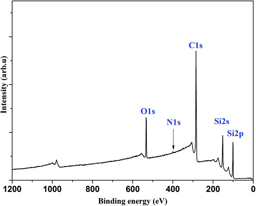 | ||
| Fig. 1 XPS scan survey of epitaxial graphene layers grown on 6H-SiC face terminated carbon 6H-SiC (000−1). | ||
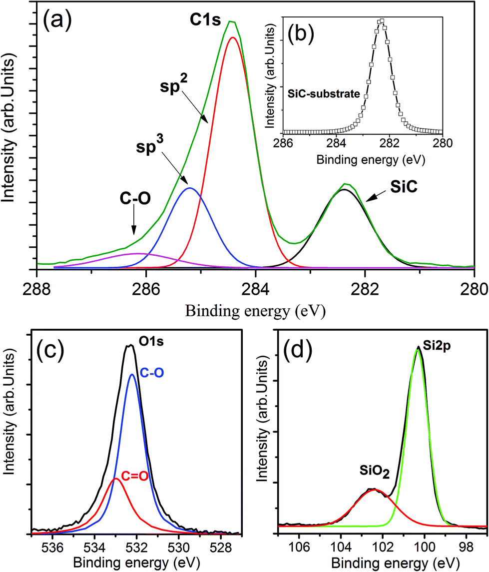 | ||
| Fig. 2 XPS components of epitaxial graphene layers grown on 6H-SiC face terminated carbon 6H-SiC (000−1) respectively (a) C 1s core level, indicating hybridization sp2 and sp3 orbitals, single C–O and Si–C bonds are also shown, (b) the 6H-SiC substrate peak prior to graphene growth, (c) the oxygen levels, deconvolution separates C–O and CO bond contributions, (d) Si 2p and SiO2 peaks. | ||
3.2 Atomic force microscopy
We have carried out atomic force microscopy (AFM) measurements in contact mode on the grown epitaxial graphene layers in order to analyse their distribution and surface roughness. Various areas of the sample were studied. Here, we report a typical sample surface within a 4.5 × 4.5 μm region (see, Fig. 3). The topography of the surface changes within a small range across the sample surface to reach a maximum of 1.5 nm (see, Fig. 3b and c). The high intensities (i.e. >1.5 nm) are mainly assigned to the presence of defects. The height profile varies on the nanometer scale, thus identifying the location of the graphene flakes. Here, different contrasts were observed, from brown to light brown to indicate the possible multiple graphene layers inside the flakes, as reported by the XPS measurements. The flake layer numbers and sizes varied depending on location.24 The graphene flakes are separated by edge zones, in the proximity of which impurities and defects are often concentrated. Such morphological behaviour in the random growth of graphene layers is a common sign of graphene grown on face terminated carbon SiC substrate.23,24 However, the AFM results show preferential orientation in the graphene layer flakes. This is mainly due to the terraced substrate surface underneath. In fact, the surface morphology of the substrate significantly affects the graphene layer. Thus, imperfection and the flatness of the substrate lead to plateau-like features that impose a particular orientation on the graphene layers. The absence of the buffer layer between the graphene and the substrate as well as the unintentional oxidation of graphene may be additional contributing factors influencing the surface appearance and the distribution of defects and impurities. Defects are normally identified by high intensities in the AFM scans (e.g. >1.5 nm) which appear white in the selected contrast (Fig. 3). The defects are frequently found near the edge zones of graphene flakes.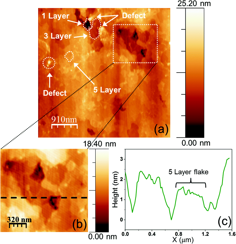 | ||
| Fig. 3 (a) AFM measurements of the graphene grown on 6H-SiC (000−1) across a surface area of 4.5 × 4.5 μm reveal the random growth of layers on the sample surface related to the face termination of the substrate. A defect as well as the suggested number of graphene layer flakes (1, 3 and 5) are indicated. (b) Magnification of the AFM image showing two graphene flakes (layer number: 5). (c) AFM topography image across the 5 layer graphene flake illustrating homogeneity across a flake. The thickness of the flake corresponds approximately to 5 layers of graphene. | ||
3.3 Raman spectroscopy analysis
We continued the analysis of our sample surface morphology using Raman spectroscopy. This technique characterises the graphene layer's properties. The sample surface image in various areas was obtained using Raman mapping. The local Raman spectra determine the degree of homogeneity of the layers by identifying the amount of defects and analysing the different graphene layers edges. For a better analysis, Raman mapping was carried out with a 0.5 μm step and an auto-focusing adjustment before each spectrum acquisition. We report Raman spectra registered at different points in the sample surface in the frequency range between 1000–3000 cm−1 (see, Fig. 4). We located all the Raman modes of the graphene, such as the D, G and 2D bands (see, Fig. 4a, b and c).25–27 The G-band is a doubly degenerate (TO and LO) phonon mode (E2g symmetry) at the Brillouin zone centre. The D-band is assigned to phonons on the K point and defects.28,29 The 2D band is associated with 2TO. We investigated the Raman mapping of the D band. The D-band spectra showed mostly low intensity (Fig. 4a). This could be associated mainly with oxygen impurities present in epitaxial graphene layers. High intensity in the D-band is normally induced by structural defects found in epitaxial graphene on face terminated carbon. The local substantial intensity maxima in D-band mapping (Fig. 4a) are believed to correspond to such structural imperfections.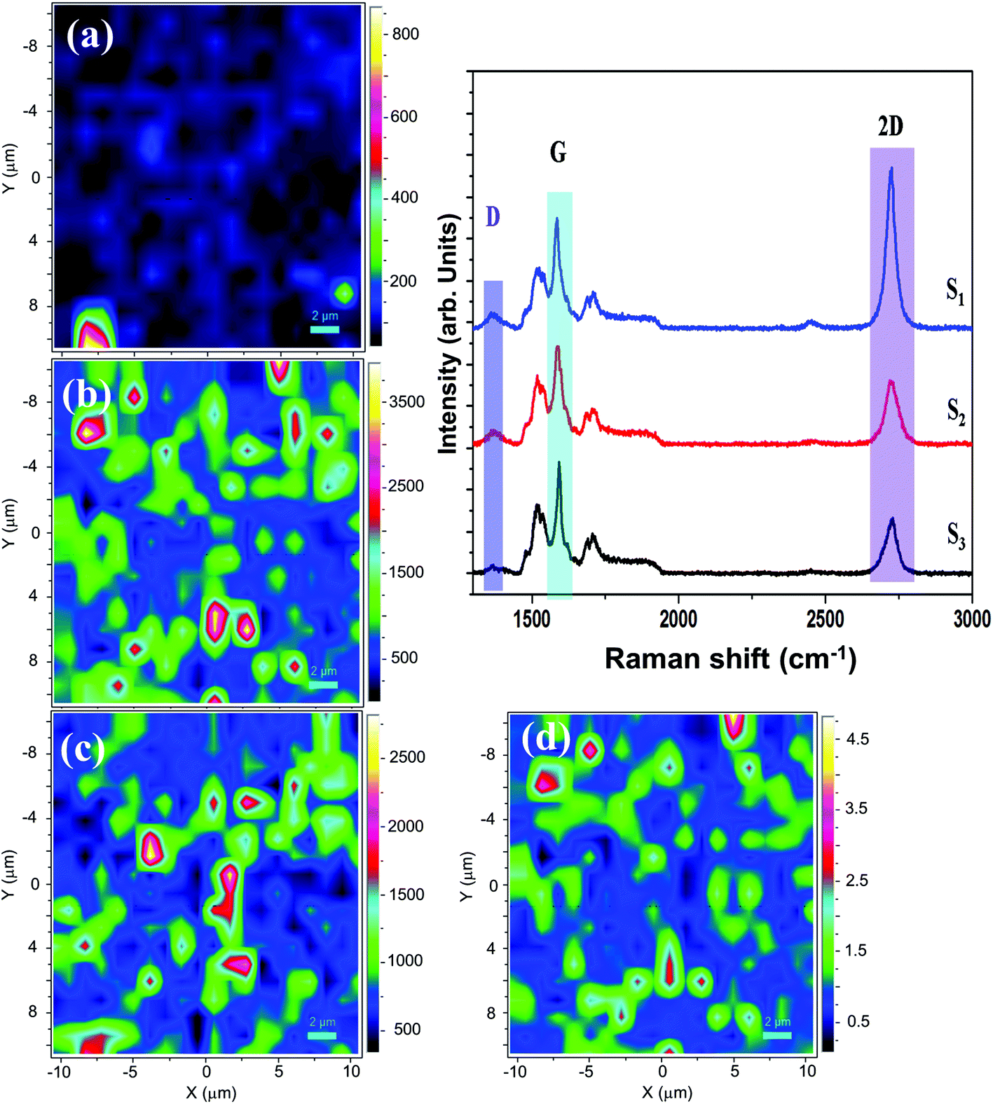 | ||
| Fig. 4 Raman spectra of epitaxial graphene in the frequency range [1000–3000 cm−1] assigned respectively to: S1 – single layer, S2 – four layers and S3 – five layers; Raman mapping intensity of (a) D band, (b) G band, (c) 2D band and (d) G band normalised by 2D band intensities IG/I2D. The ratio intensity illustrates the corresponding graphene layer numbers n (intensity ratio < 0.5 implies n = 1, intensity ratio ∼1.5, n = 4). | ||
The graphene layer number distribution across the surface was investigated by comparing the associated Raman mapping intensity of the G and 2D bands, respectively, at the frequencies ωG and ω2D (see, Fig. 4b and c). The intensity ratio of the G and 2D bands (IG/I2D) identify the local layer numbers. Conventionally, an IG/I2D ratio of <0.5 corresponds to single layer graphene (n = 1), a ratio of 1.5 relates to four-layer graphene (n = 4) and a ratio of 2 denotes five-layer graphene (n = 5).30,31 Here, the IG/I2D ratio varies between 0.2–4. Various graphene flakes were located and mainly single (n = 1), four- (n = 4) and five- (n = 5) layer coverage was found (see, Fig. 4d). However, a negligible amount of graphite flakes (IG/I2D = 2.5, n > 5) were also located.31,32 From the mapping intensities the graphene flakes appear to be randomly distributed. Nevertheless, the graphene quality in each flake is highly homogeneous. The flakes have common dimensions of 2 μm × 2 μm. The multiple overlapping graphene flakes contribute to the non-homogeneity of the graphene film composition. The flake edges provide a sharp contrasting difference in the intensity maps and also define the edge zones between the layers (Fig. 4a). Interestingly, a large amount of defects appear to be concentrated at or near the edge zones. The presented combined Raman analyses are in good agreement with the XPS and the AFM data, identifying up to five-layered graphene flakes. The AFM measurements, in particular, highlight the random distribution of the graphene layers. The Raman spectra create a visual map of the defects across the sample surface, revealing their dominant presence mainly at the edge zones of the graphene layers.
4. Results and discussion
4.1 Epitaxial graphene photoresistance “EGP”
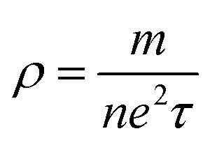
The time dependence of the electrical resistance in epitaxial graphene under continuous irradiation with light demonstrates unique physical characteristics. This Epitaxial Graphene Photoresistance (EGP) is strongly dependent upon the wavelength of the applied light source. The light illumination has been produced with the use of three lasers having different wavelengths: λ = 409 nm (violet), λ = 515 nm (green) and λ = 625 nm (red), respectively. For these wavelengths the dependence of the EGP on time is given in Fig. 5a. In order to prevent any heating effect we used lasers with a low comparable power of less than 1 mW. The photoresistance experiments were conducted on epitaxial graphene grown on 6H-SiC face terminated carbon “6H-SiC (000−1)”. A conventional 4-probe method was used for electrical resistance measurements. The optical image of the sample with four contacts attached in a linear configuration is shown in Fig. 5b. The most significant EGP effect was observed under violet light irradiation (λ = 405 nm), where the energy of the photons is close to the band gap in the 6H-SiC substrate (≈3.03 eV, λ = 409 nm). For wavelengths with lower energy (λ > 409 nm) such as green (λ = 515 nm) and red (λ = 625 nm) light, little to no EGP effect was expected, as the photon energy lies directly in the 6H-SiC substrate gap. However, surprisingly, even in these cases (green and red light) a measurable EGP signal was detected that saturated with time (Fig. 5a). In comparison, irradiation with red and green light produced approximately a fifth of the photo-response obtained by irradiation with violet light. It is natural to assume that in order to generate photo-resistance “PR”, the photon energy should be larger than the SiC bandgap, which makes the observation of an EGP under red and green light quite remarkable.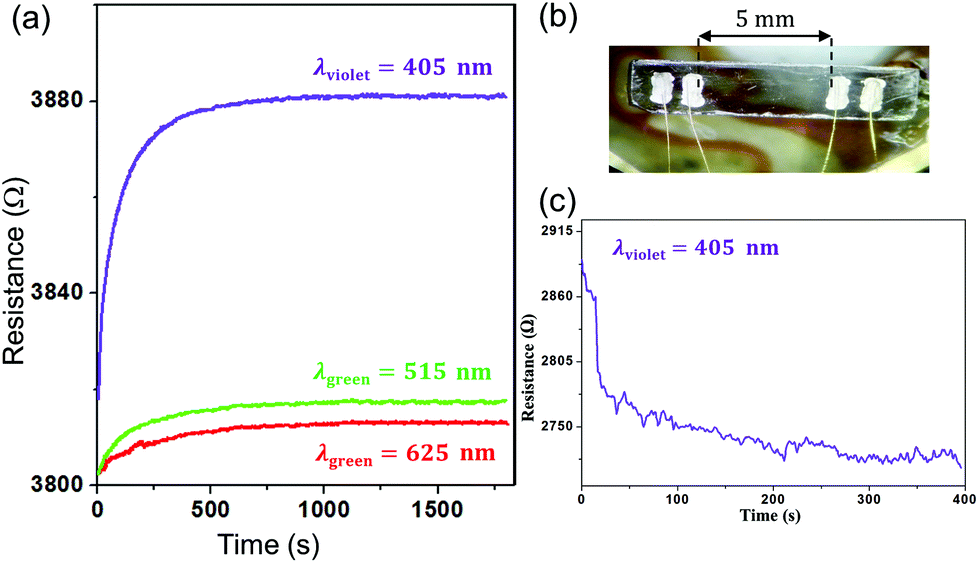 | ||
| Fig. 5 (a) The time dependence of the photoresistance of epitaxial graphene grown on 6H-SiC face terminated carbon (000−1), under continuous light irradiation: the purple, green and red curves correspond to the different illumination photon frequencies, from violet (405 nm), green (515 nm) and red (625 nm) lasers respectively; (b) optical image of the sample highlighting the four-probe contacting method for resistance measurements; (c) the time dependence of the photoresistance of a 6H-SiC substrate without graphene control, taken under continuous light irradiation from a violet laser. Notably, the time dependence of the substrate alone is negative, in sharp contrast to the graphene. | ||
A possible explanation for this could be related to the sensitivity of the graphene layers to the underlying substrate, which imposes constraints on its electrical properties.4,12 For example, any insulating substrate has impurities and defects which may localise electrons and holes in the gap. Indeed, SiO2 flakes contain natural structural defects near the substrate surface which act similarly to impurities. They produce a Lifshitz tail in the electron density of states. We consider only dopants with energy levels close to the conduction and valence bands of the SiC substrate. Thus, photon energies close to the SiC defect/impurity band gap become potentially sufficient to trigger a PR and produce an electrical current. Graphene is highly sensitive to the type of substrate, where lattice imperfections can lead to local charge redistribution between graphene and the substrate. For epitaxial graphene the band structure of the SiC substrate is modified in proximity to the graphene layer. This results in the bending of the conduction and valence bands in SiC creating charged depletion centres in the vicinity of the graphene with an internal electrical field directed perpendicular to the graphene plane. The electrons and holes induced by the light irradiation move in this field in opposite directions: towards and away from graphene or vice versa, respectively. The latter depends on the deformation of the bands with respect to the Dirac point of the graphene layer. The situation is similar to a Schottky barrier on a contact between a semiconductor and a metal. The Schottky barrier causes band distortion and Lifshitz tail formation effectively reducing the band gap, which allows electrons to be excited from the valence band under illumination from light, with photon energies below the energy gap of the semiconductor. The electrons and holes, which are created by light, can also become trapped in the charged barrier area.
The epitaxial graphene on SiC provides a unique system where unconventional photoeffects can occur. The EGP response varies between 3818–3880 Ω. Although the electrical resistance changes by about 2%, the observed effect is persistent and very surprising. Indeed, graphene photoresponses examined so far in the literature appear only under excitation energy of 4.7 eV (λ ≈ 260 nm) in the vicinity of the M point, which corresponds to the ultraviolet and terahertz domains. Furthermore, our epitaxial graphene effects are the opposite to what is commonly known and expected in the visible domain in other photo-responsive materials; in the EGP the resistance change is positive. This paper presents the first experimental observations of an increased photo-resistance in epitaxial graphene under exposure to visible light (Fig. 5a).
As a control experiment the PR was measured for the 6H-SiC (000−1) substrate (Fig. 5c). The substrate was illuminated with violet light (λ = 405 nm) and a negative PR response was observed, as expected for a semiconductor. The conventional decrease in photoresistance under light illumination generally occurs due to an increase in the current carrier density. The photoresistance of SiC without graphene decreases under continuous light excitation. The observed effect is about 6% and saturates more rapidly than in the graphene system. Thus, the exposure of the pure substrate to violet light enhances the carrier density, and dramatically decreases the resistance. The effect can be simply described with a one band Drude model, where the electron resistance is given by the following expression:
 | (1) |
In the newly discovered EGP the resistance increases under light excitation.33,34 To explain these findings we postulate that the light irradiation produces charge carriers and localised charge centres. The proposed charge inhomogeneity may originate due to the trapping of electrons and holes created by light by oxygen impurities and by defects both in the graphene and in the SiC and SiO2 flakes. Note that, we do not expect a change in the oxygen impurities under light illumination. In fact, we have checked the oxygen content before and after light illumination using XPS measurement and detected no changes. All photo-resistance experiments were conducted under conditions of high vacuum with no significant effects of humidity and air oxygen on the sample surface. The presence of impurities and defects suggested here are likely to be the result of the graphene growth and preparation process.
Intentionally oxidised epitaxial graphene is characterised by a stable state that is unchanged under light illumination. For example, oxygen impurities on graphene can trap electrons and therewith induce a high density of negatively charged centres. Due to the Coulomb interaction the current carriers scatter on these centres and the scattering time τ decreases, leading to a corresponding increase in resistance. In other words, the epitaxial graphene becomes n-doped while the substrate remains unintentionally p-doped. The resulting charge redistribution between the graphene and the SiC substrate creates an electric field in the depletion area near the graphene which directs the migration of electrons or holes. Depending on the electron/hole transport this affects the current carrier density n as well as the position of the Fermi level in the graphene. The observed EGP behaviour may arise mainly due to two factors: (1) the decrease in the Fermi energy of the graphene; (2) the creation of a new scattering mechanism associated with the light irradiation. The new proposed scattering mechanism could be related to the morphological imperfection of the epitaxial graphene layers, such as: impurities, defects, grain boundaries and edge zones between the layers that may act as traps for electrons or holes. Similarly, the presence of SiO2 flakes – small insulator islands – may form barriers to electron migration between the substrate and graphene, leading to charge redistributions that affect scattering, electrical transport and current carrier density.
Additionally, the unintentional oxidation of the graphene films may play an equally important role in the observed effect. Oxygen impurities inside the graphene may also isolate excited electrons and holes from each other, contributing to charge centre formations. Fig. 6 describes the resistance increase mechanism for monolayer graphene, which could be generalised for multiple-number graphene layers.
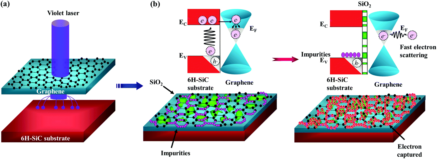 | ||
| Fig. 6 Photoresponse process: (a) initial state of epitaxial graphene i.e. at equilibrium, (b) violet laser irradiation of the sample surface, creating charged centres on impurities and defects, leading to the trapping and scattering of electrons and holes. The modified band structure and unconventional electron transport result in novel photoresistance and photovoltage effects. | ||
In order to verify the importance of oxygen impurities in this new EGP effect, we have investigated samples of ordinary epitaxial graphene grown on 4H-SiC face terminated carbon (4H-SiC (000−1)). The photoresponse of non-oxidised multi-layer (n > 5) epitaxial graphene grown on 4H-SiC (000−1) is reported in the ESI.† In this control experiment the photo-resistance in graphene shows a decrease in resistance upon illumination as expected for a conventional semiconductor. Both studied graphene samples (6H-SiC and 4H-SiC) are grown on face terminated carbon, and are subject to a similar level of morphological imperfections such as defects and multi-layer graphitization. The main difference between the samples could be in the number of oxygen impurities which also affect the formation and nucleation of graphene flakes. In fact, oxygen impurities become more localised at the flake edges or edge zones of the layers, as observed in AFM and Raman measurements. As a result Coulomb effects may become important for electron transport. Therefore, we conclude that oxygen impurities may be the main origin of the photoresistance phenomenon observed here. The one band Drude model could be modified accordingly to take in the contribution from the impurities:
 | (2) |
4.2 Resistance and magnetoresistance in epitaxial graphene
The temperature dependence in non-illuminated epitaxial graphene was studied across a temperature range 4–300 K. The cryogenic temperatures were reached in a pulse-tube cryo-cooler with minimal vibration effects. The resistance exhibits a descending tendency, where it decreases from 6828–3841 Ω across the measured temperature range (Fig. 7a). This corresponds to a change in resistance of about 40%, which is unusually large, as for example ordinary graphene normally demonstrates a resistance change of about 7% over the same temperatures. Graphene quantum dots report similar resistance changes as the ones observed here.36,37 Here, as temperature decreases the number of excited electrons also decreases while the resistance increases. In fact, epitaxial graphene layers are characterised by their high roughness produced by the existence of different domain sizes i.e. grains. This becomes pronounced for the face terminated carbon, where various numbers of layers may exist in the same area (see, Fig. 3). The various grain sizes and graphene layer flakes enhance local impurity effects due to oxygen, and defects. These morphological imperfections become pronounced with the presence of SiO2 flakes in-between the graphene layers and at the top layer of the SiC substrate. In fact, various resistive interface regions will be formed at the edges of the graphene layers where a significant amount of impurities reside.38 The temperature dependence of the electron transport will be significantly affected by the sample inhomogeneity.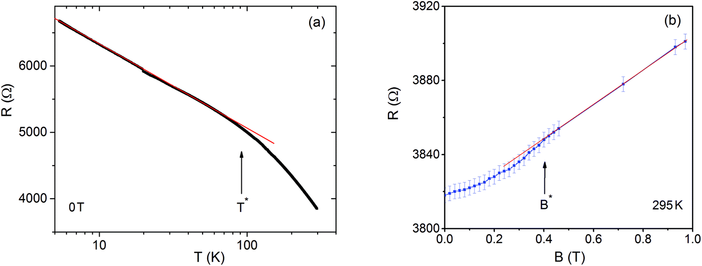 | ||
| Fig. 7 (a) Temperature dependence of the resistance in non-illuminated epitaxial graphene layers grown on 6H-SiC (000−1) between 4–300 K. At low temperature 4–100 K the resistance follows a strong logarithmic behaviour. The crossover temperature T* characterising the deviation from the logarithmic dependence is indicated and corresponds approximately to T* ∼ 100 K. (b) Magnetoresistance in epitaxial graphene at 295 K in a magnetic field between 0–1 T. Until a field of B* ∼ 0.4 T the magnetoresistance is quadratic in field. The logarithmic low-temperature resistance as well as the quadratic magnetoresistance are consistent with the Altshuler–Aronov effect. Surprisingly for fields exceeding B > 0.4 T the magnetoresistance changes to a pronounced linear dependence. | ||
In the present experimental results the increasing dependence of the resistance on logarithmic temperature at low temperatures is most remarkable (Fig. 7a). This behaviour persists over a broad range of temperatures below a crossover temperature T* ∼ 100 K, showing no signs of saturation at 4 K.
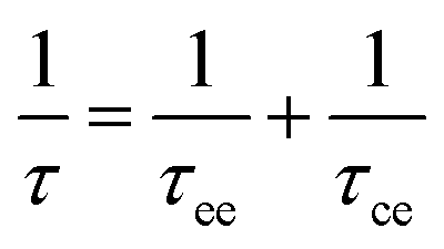
Similar logarithmic temperature behaviour for resistivity has been reported recently for graphene with irradiation-induced vacancies.39 In the paper it was argued that persistent orbital currents develop around the vacancies inducing on-site local magnetic orbital moments. The orbital moments couple to the conduction electrons via the Kondo effect. Extensive discussions within the community prevent the reaching of a consensus on this topic. It was proposed that the observed logarithmic temperature dependence may be related to the well-known Altshuler–Aronov (AA) effect,40 which introduces corrections into the resistivity of the form
 | (3) |
The logarithmic (AA) temperature fitting of the resistance data to eqn (3) provides a transport momentum relaxation time of τtr = 10−15 s. Through conventional estimation, assuming that the Fermi velocity in graphene is vF ∼ 106 m s−1, this translates to a mean free path of l ∼ 10 Å which is equivalent to several graphene rings. The A-constant cannot be extracted as the geometric factor for converting resistance R to resistivity ρxx is not accurately known.
According to the equation by Altshuler–Aronov (eqn (3)) the magnetoresistance should be positive and follow a quadratic field-dependence ∼B2. For comparison, the case of graphene with irradiated vacancies which satisfied the logarithmic temperature behaviour showed small, negative, nearly field-independent magnetoresistance at low temperature which cannot be explained by the AA correction terms.39 The magnetoresistance in the present graphene samples (consisting of multiple flakes) in fields up to 1 T at a temperature of 295 K is presented in Fig. 7b. Interestingly, the magnetoresistance in this system is positive with the characteristic quadratic field-dependence for fields below B* < 0.4 T, consistent with the AA effect. Fitting to the quadratic behaviour below 0.4 T allows the determination of the mobility parameter for the present graphene. The mobility in this type of graphene is calculated as μ = 3000 cm2 V−1 s−1. This value is comparable to other mobility studies in graphene.4,46
The situation changes significantly at fields greater than B* > 0.4 T when a linear field-dependent magnetoresistance is observed for multi-flake graphene in sharp contrast with the Altshuler–Aronov predictions (Fig. 7b). Consequently, although we observe logarithmic temperature variation in resistance at low temperatures consistent with the previous literature, and quadratic field dependence of the magnetoresistance at low fields at room temperature, the unusual change in magnetoresistive properties at high magnetic fields disputes the AA effect as the sole origin of this behaviour.
The Altshuler–Aronov effect may certainly be a contributing factor, but an additional source of the logarithmic R(T) may lie in a “Kondo”-like contribution to the scattering processes, due to persistent current-induced orbital moments.39 In the present graphene sample it is likely that with the applied magnetic field persistent currents may develop and flow in the graphene layer, leading to topological two-phase properties. The existence of linear magnetoresistance may also indicate that our system is disordered and instead of well localised vacancies as in Chen et al.39 we may have persistent current confined along the edges of the graphene flakes. Consistent with the experimental measurements, these persistent current loops dynamically localize the conduction electrons, leading to an increased resistance R in the field (positive magnetoresistance) as well as slower decay time in the illuminated graphene specimens (Fig. 8c & d). As shown by Bulgadaev & Kusmartsev the linear magnetoresistance may result from a creation of the two phase system with different electron mobilities.47
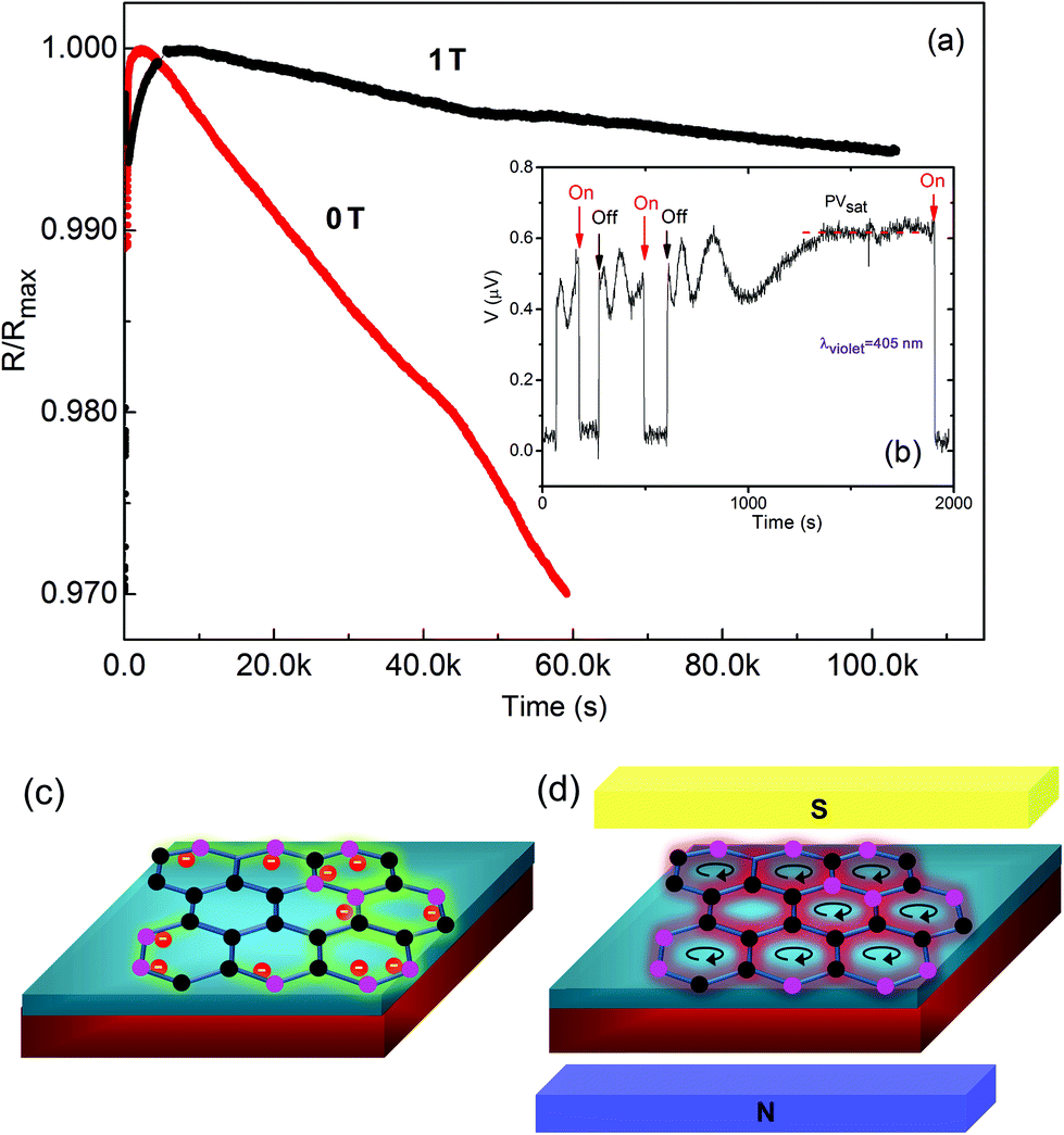 | ||
| Fig. 8 (a) Photoresistance decay time without a magnetic field effect (B = 0 T) and with magnetic field (B = 1 T). (b) Photovoltage measurements of epitaxial graphene layers grown on 6H-SiC (000−1) under violet laser excitation. The red lines indicate the case of the laser (on), while black lines correspond to the switch off of the laser. The saturation voltage reaches values of PVsat ∼ 0.6 μV for λ = 405 nm laser. (c) Excitation of electrons from the EV to EC of the 6H-SiC substrate and migration of the electrons to the graphene layers (locations of vacancies/impurities are indicated in pink). (d) Trapping of holes by vacancies and impurities which induces persistent currents around flake edges and correspondingly a short transport relaxation time τtr under a magnetic field. Together, these lead to positive magnetoresistance and considerably slowed decay times in magnetic fields as shown in (a). | ||
An alternative interpretation of the logarithmic temperature dependence of resistivity was suggested by Kusmartsev & Tsvelik who explored spin–orbital and electron–electron interactions in two-dimensional systems having a Dirac electron spectrum arising in a contact of two semiconductors with mutually-inverted band structures.1 Their predictions show a decrease in resistivity with decreasing temperature.1 The authors further demonstrated that the inclusion of the additional contribution of the Coulomb electron–electron interaction significantly changes its character. This is particularly relevant for heterogeneous structures with low dimensions. Therefore, the observed effect (Fig. 7a) may occur due to Coulomb-enhanced electron–electron interaction (EEI),48 which in the diffusive regime also gives a logarithmic correction to the resistance, particularly in two-dimensional systems.
4.3 Magnetic dependence of photoresistance decay
In order to achieve a consistent description of the impurities (defects)-related lifetime degradation, we investigated epitaxial graphene photoresistance decay under magnetic fields (Fig. 8a). These measurements reveal that the electron recombination process strongly depends on the local structural defects and magnetic field presence. We measure the resistance variation under the influence of an applied magnetic field. We began by illuminating the sample surface by the violet laser until a stable value of the resistance was reached. At this level the resistance decay was recorded as the light turned off in two cases: (1) without the magnetic field and (2) with a high magnetic field B = 1 T. These two studied cases have very different time-dependent behaviour. Fig. 8a represents the photoresistance excitation and decay. So far we have described the photo-excitation of epitaxial graphene above. Here, we will focus on the relaxation process occurring in these cases, with and without a magnetic field. Without the magnetic field the relaxation time is relatively shorter. Here, excited electrons recombine faster. On the other hand even here the relaxation process takes a significantly longer time (τ ≈ 17 hours) than that with an ordinary semiconductor. Such a long decay time of the excited charge carriers in the graphene layers may be associated with lattice defects, including the surface states. Thus, the electrons may not recombine directly, especially with the current morphological properties of epitaxial graphene. There may exist various relaxation processes. In fact, epitaxial graphene is characterised by its roughness, high amount of defects, high oxygen impurities and grain boundaries between the graphene flakes. These all increase the electron life-time in the graphene layers. On the other hand, the decay time or the process of the photoresistance decay observed under a magnetic field is much longer than that without the magnetic field. Note that a magnetic field usually has a dramatic influence on graphene flakes.49–51 In a magnetic field the graphene flakes transform into topological insulators. The topological state is characterised by the formation of persistent currents on flake edges52,53 and the corresponding opening of an insulating gap inside their bulk. Because of this gap in the energy spectrum the relaxation is slowed down. In the bulk the charges are localised and resist taking part in the recombination process. Here photoresistance decay is mainly associated with non-uniform edge persistent currents53 where the mobile charge carriers are concentrated near the flake edges (Fig. 8c & d). Therewith, the magnetic field then slows down the recombination processes between the electrons and holes. Therefore, because of the complex topology of the edge persistent currents, the relaxation process cannot be generally described by a single exponential function. Note that this is also the case for a zero magnetic field. In both cases a decay of photoresistance follows some power-law (or linear) function which cannot be described by a single relaxation time. In this paper, we do not discuss the decay shape or details of the decay process. Here the magnetic measurements highlight the role of the morphological imperfections in epitaxial graphene. The observed behaviour demonstrates the dramatic reduction of the charge recombination rate under a magnetic field, as we expected, since the graphene flakes became topologically insulating. Here, the photoresistance decay lasts significantly longer. Under the magnetic field the edge currents are formed or enhanced and all mobile electrons are expelled from the bulk to the edges of the graphene flakes, where most of the defects exist.50,52,53 The magnetic field enhances the Coulomb interaction between excited electrons and separates hole and electron charge carriers. Both factors slow down the recombination rate between holes and electrons, leading to longer decay times τ. Other elementary excitations, like phonons, may need to be included to attain a fuller understanding of the mechanisms involved.Moreover, we argue that a similar transformation of the graphene flakes into topological insulators is responsible for the magnetoresistance (MR) observed here (see, Fig. 7b). Here we see that the MR increases nearly linearly when the magnetic field rises from 0.4 to 1 T. We argue that this MR increase is associated with the creation of persistent currents which form a nontrivial topology. In fact, such a linear increase of the MR may be associated with a formation of a two phase system.47 Here the two phase system is dictated by the nature of the topological insulator created from the graphene flakes by a magnetic field. The bulk of the flake is insulating and the edges are conducting. Thus, the magnetoresistance and photo-resistance decay time measurements are complementary, highlighting the nontrivial effects and the photo-physical properties of epitaxial graphene.
4.4 Epitaxial graphene photovoltage time dependence “EGPVTD”
Motivated by the unique photoresistance response, we have examined the photovoltage effect. We have presented epitaxial graphene photovoltage time dependence “EGPVTD”. To the best of our knowledge the EGPV has not been reported to date in the literature. The photovoltage responses investigated here were examined in detail under violet laser (λ = 409 nm) illumination, for reasons as argued above. Fig. 8b depicts the EGPVTD signal recorded with (on) and without (off) photo-excitation. The EGPVTD response shows pronounced oscillations saturating at about 6 × 10⁻⁷ V at extended time intervals (1200 s). Here, electrons are excited from surface states towards the conduction band, which causes a decrease in the deflection of bands in the surface regions. These electrons, after reaching the conduction band of the SiC substrate, pass to the graphene layers to occupy new levels of energies. This in turn causes an increase in the PV value.34 At this stage, excited electrons undergo scattering interactions on approaching a quasi-equilibrium state inside the system. In the quasi-equilibrium state the photovoltage value finally saturates and becomes constant. The fluctuations in the photo-voltage may be attributed to the trapping of electrons by impurities. A quasi-periodic EGPV signal behaviour was observed over several time intervals, such as 60 s, 200 s and 1500 s. However, the voltage becomes stable after 1500 s, highlighting the system settling into a quasi-equilibrium state. This equilibrium state could also be verified from the EGP measurements, where the resistance reaches its maximum for time constants exceeding 1200 s (see, Fig. 5a). However, the fluctuations of the excited electrons are better seen as oscillations in the EGPVTD measurements.5. Conclusions
In summary, we have revealed new photoresistance and photovoltage responses in epitaxial graphene grown on 6H-SiC face terminated carbon (6H-SiC (000−1)). For the first time, we showed that epitaxial graphene photoresistance increases under light illumination. Detailed measurements were done for a violet laser of wavelength λ = 409 nm due to its close energy to the 6H-SiC substrate gap. We have observed the most prominent photo-response in graphene grown on the C-terminated 6H-SiC substrate, which we believe to be due to the non-trivial roughness of its surface topology. We argue that the observed effects are associated with the morphological imperfections characterising the epitaxial layers grown on face terminated carbon. Here a range of measurement techniques were used: X-ray photoelectron spectrometry, atomic force microscopy, Raman spectroscopy, and magneto-photoresistance decay analyses. We expect that our findings may attract attention towards photovoltaic applications of the epitaxial graphene oxide grown on face terminated carbon, despite its random growth and well known imperfections. Here, we have shown that its morphological texture is responsible for the creation of its unique photo-effects. These stable, long-lifetime phenomena create the possibility of using epitaxial graphene in new photodetector technologies.Acknowledgements
We thank Dr Abdelkarim Ouerghi from CNRS (Laboratoire de Photonique et de Nanostructures (LPN)) for providing the investigated samples and Dr Pat Cropper (Department of Materials, Loughborough University, Loughborough, UK) for assistance in preparing the XPS measurements. The authors thank the EPSRC for funding under a KTA grant – “Developing prototypes and a commercial strategy for nanoblade technology”. The data found in this paper can be obtained in ref. 54.References
- F. V. Kusmartsev and A. M. Tsvelik, JETP Lett., 1985, 42, 257 Search PubMed.
- A. K. Geim and K. S. Novoselov, Nat. Mater., 2007, 6, 183 CrossRef CAS PubMed.
- W. Li, B. Chen, C. Meng, W. Fang, Y. Xiao, X. Y. Li, Z. F. Hu, Y. X. Xu, L. Tong, H. Q. Wang, W. T. Liu, J. M. Bao and Y. R. Shen, Nano Lett., 2014, 14, 955 CrossRef CAS PubMed.
- Y. P. Wu, B. Wang, Y. F. Ma, Y. Huang, N. Li, F. Zhang and Y. S. Chen, Nano Res., 2010, 3, 661 CrossRef CAS.
- W. S. Kim, Y. I. Kim, H. J. Kim, J. Y. Hwang, S. Y. Moon, N. H. Park, K. B. Shim, H. W. Kim, H. Ham and H. Huh, J. Mater. Chem., 2011, 21, 15655 RSC.
- H. W. Tien, Y. L. Huang, S. Y. Yang, J. Y. Wang and C. C. M. Ma, Carbon, 2011, 49, 1550 CrossRef CAS.
- Q. Liu, Z. F. Liu, X. Y. Zhang, N. Zhang, L. Y. Yang, S. G. Yin and Y. S. Chen, Appl. Phys. Lett., 2008, 92, 223303 CrossRef.
- L. Sun, C. G. Tian, M. T. Li, X. Y. Meng, L. Wang, R. H. Wang, J. Yin and H. G. Fu, J. Mater. Chem. A, 2013, 1, 6462 CAS.
- K. V. Emtsev, A. Bostwick, K. Horn, J. Jobst, G. L. Kellogg, L. Ley, J. L. McChesney, T. Ohta, S. A. Reshanov, J. Röhrl, E. Rotenberg, A. K. Schmid, D. Waldmann, H. B. Weber and T. Seyller, Nat. Mater., 2009, 8, 203–207 CrossRef CAS PubMed.
- A. O′Hare, F. V. Kusmartsev and K. I. Kugel, Nano Lett., 2012, 12, 1045 CrossRef PubMed.
- N. Srivastava, G. He, Luxmi, P. C. Mende, R. M. Feenstra and Y. Sun, J. Phys. D: Appl. Phys., 2012, 45, 154001 CrossRef.
- Y. Shi, W. Fang, K. Zhang, W. Zhang and L.-J. Li, Small, 2009, 5, 2005–2011 CrossRef CAS PubMed.
- J. Penuelas, A. Ouerghi, D. Lucot, C. David, J. Gierak, H. Estrade-Szwarckopf and C. Andreazza-Vignolle, Phys. Rev. B: Condens. Matter, 2009, 79, 033408 CrossRef.
- Z. Ni, Y. Wang, T. Yu and Z. Shen, Nano Res., 2008, 1, 273–291 CrossRef CAS.
- N. Aghdassi, D. Dulson, S. Linden, L. Li, L. Chi and H. Zacharias, Appl. Surf. Sci., 2012, 258, 7280–7285 CrossRef CAS.
- L. B. Biedermann, M. L. Bolen, M. A. Capano, D. Zemlyanov and R. G. Reifenberger, Phys. Rev. B: Condens. Matter, 2009, 79, 125411 CrossRef.
- L. I. Johansson and C. Virojanadara, J. Mater. Res., 2014, 29(3), 426–438 CrossRef CAS.
- C. E. Giusca, S. J. Spencer, A. G. Shard, R. Yakimova and O. Kazakova, Carbon, 2013, 69, 221–229 CrossRef.
- S. Drewniak, R. Muzyka, A. Stolarczyk, T. Pustelny, M. Kotyczka-Moranska and M. Setkiewicz, Sensors, 2016, 16, 103 CrossRef PubMed.
- F. Wang, G. Liu, S. Rothwell, M. Nevius, A. Tejeda, A. TalebIbrahimi, L. C. Feldman, P. I. Cohen and E. H. Conrad, Nano Lett., 2013, 13, 4827–4832 CrossRef CAS PubMed.
- A. Ben Gouider Trabelsi, F. V. Kusmartsev, B. J. Robinson, A. Ouerghi, O. E. Kusmartseva, O. V. Kolosov, R. Mazzocco, M. Gaifullin and M. Oueslati, Nanotechnology, 2014, 25, 165704 CrossRef PubMed.
- E. Velez-Fort, C. Mathieu, E. Pallecchi, M. Pigneur, M. G. Silly, R. Belkhou, M. Marangolo, A. Shukla, F. Sirotti and A. Ouerghi, ACS Nano, 2012, 6, 10893 CAS.
- F. Joucken, Y. Tison, P. Le Fevre, A. Tejeda, A. TalebIbrahimi, E. Conrad, V. Repain, C. Chacon, A. Bellec, Y. Girard, S. Rousset, J. Ghijsen, R. Sporken, H. Amara, F. Ducastelle and J. Lagoute, Sci. Rep., 2015, 5, 14564 CrossRef CAS PubMed.
- W. A. de Heer, C. Berger, X. Wu, M. Sprinkle, Y. Hu, M. Ruan, J. A. Stroscio, P. N. First, R. Haddon and B. Piot, Appl. Phys., 2012, 43, 37 Search PubMed.
- M. Dresselhaus, G. Dresselhaus, R. Saito and A. Jorio, Phys. Rep., 2005, 409, 47–99 CrossRef.
- D. Graf, F. Molitor, K. Ensslin, C. Stampfer, A. Jungen, C. Hierold and L. Wirtz, Nano Lett., 2007, 7, 238–242 CrossRef CAS PubMed.
- Y. Y. Wang, Z. H. Ni, Z. X. Shen, H. M. Wang and Y. H. Wu, Appl. Phys. Lett., 2008, 92, 043121 CrossRef.
- A. C. Ferrari, J. C. Meyer, V. Scardaci, C. Casiraghi, M. Lazzeri, F. Mauri, S. Piscanec, D. Jiang, K. S. Novoselov, S. Roth and A. K. Geim, Phys. Rev. Lett., 2006, 97, 187401 CrossRef CAS PubMed.
- Z. Luo, T. Yu, K.-J. Kim, Z. Ni, Y. You, S. Lim, Z. Shen, S. Wang and J. Lin, ACS Nano, 2009, 3, 1781–1788 CrossRef CAS PubMed.
- N. Z. Wang and J. Liu, Appl. Phys. A: Mater. Sci. Process., 2011, 105, 341–345 CrossRef.
- A. Ben Gouider Trabelsi, F. V. Kusmartsev, D. M. Forrester, O. E. Kusmartseva, M. B. Gaifullin, P. Cropper and M. Oueslati, J. Mater. Chem. C, 2016, 4, 5829–5838 RSC.
- C. Li, D. Li, J. Yang, X. Zeng and W. Yuan, J. Nanomater., 2011, 2011, 319624 Search PubMed.
- C. Yan, J. Wang and P. S. Lee, ACS Nano, 2015, 9(2), 2130–2137 CrossRef CAS PubMed.
- K. J. Tielrooij, L. Piatkowski, M. Massicotte, A. Woessner, Q. Ma, Y. Lee, K. S. Myhro, C. N. Lau, P. Jarillo-Herrero, N. F. van Hulst and F. H. L. Koppens, Nat. Nanotechnol., 2015, 10, 437–443 CrossRef CAS PubMed.
- R. L. Liboff, Introductory Quantum Mechanics, Addison-Wesley, 1998, p. 805 Search PubMed.
- Y. Liu, Z. Liu, W. S. Lew and Q. J. Wang, Nanoscale Res. Lett., 2013, 8, 335 CrossRef PubMed.
- Q. Shao, G. Liu, D. Teweldebrhan and A. A. Balandin, Appl. Phys. Lett., 2008, 92, 202108 CrossRef.
- Y. Gong, M. Long, G. Liu, S. Gao, C. Zhu, X. Wei, X. Geng, M. Sun, C. Yang, L. Lu and L. Liu, Phys. Rev. B: Condens. Matter, 2013, 87, 165404 CrossRef.
- J.-H. Chen, L. Li, W. G. Cullen, E. D. Williams and M. S. Fuhrer, Nat. Phys., 2011, 7, 535–538 CrossRef CAS.
- B. L. Altshuler, A. G. Aronov and P. A. Lee, Phys. Rev. Lett., 1980, 44, 1288–1291 CrossRef CAS.
- A. A. Kozikov, A. K. Savchenko, B. N. Narozhny and A. V. Shytov, Phys. Rev. B: Condens. Matter, 2010, 82, 075424 CrossRef.
- B. Jouault, B. Jabakhanji, N. Camara, W. Desrat, C. Consejo and J. Camassel, Phys. Rev. B: Condens. Matter, 2011, 83, 195417 CrossRef.
- S. Lara-Avila, A. Tzalenchuk, S. Kubatkin, R. Yakimova, T. J. Janssen, K. Cedergren, T. Bergsten and V. Falko, Phys. Rev. Lett., 2011, 107, 166602 CrossRef PubMed.
- J. Jobst, D. Waldmann, I. V. Gornyi, A. D. Mirlin and H. B. Weber, Phys. Rev. Lett., 2012, 108, 106601 CrossRef PubMed.
- J. Jobst and H. B. Weber, Nat. Phys., 2012, 8, 352–352 CrossRef CAS.
- C. Berger, Z. Song, X. Li, X. Wu, N. Brown, C. Naud, D. Mayou, T. Li, J. Hass, A. N. Marchenkov, E. H. Conrad, P. N. First and W. A. de Heer, Science, 2006, 312, 1191–1196 CrossRef CAS PubMed.
- S. A. Bulgadaev and F. V. Kusmartsev, Phys. Lett. A, 2005, 342, 188–195 CrossRef CAS.
- B. L. Altshuler and A. G. Aronov, in Electron-Electron Interactions in Disordered Systems, ed. A. L. Efros and M. Pollak, North Holland, 1985, p. 628 Search PubMed.
- V. Krstic, D. Obergfell, S. Hansel, G. L. J. A. Rikken, J. H. Blokland, M. S. Ferreira and S. Roth, Nano Lett., 2008, 8, 1700–1703 CrossRef CAS PubMed.
- Y. Liu, R. P. Tiwari, M. Brada, C. Bruder, F. V. Kusmartsev and E. J. Mele, Phys. Rev. B: Condens. Matter, 2015, 92, 235438 CrossRef ; (also see the references therein).
- D. M. Forrester and F. V. Kusmartsev, Nanoscale, 2014, 6, 7594–7603 RSC.
- F. V. Kusmartsev, Phys. Rev. B: Condens. Matter, 1995, 52, 14445–14456 CrossRef CAS.
- F. V. Kusmartsev, JETP Lett., 1991, 53, 28–30 Search PubMed.
- A. Ben Gouider Trabelsi, F. V. Kusmartsev, M. B. Gaifullin, D. M. Forrester, A. Kusmartseva and M. Oueslati, Nanoscale, 2017 DOI:10.17028/rd.lboro.4986233.
Footnote |
| † Electronic supplementary information (ESI) available: XPS and photoresistance measurements for graphene grown on 4H-SiC. See DOI: 10.1039/c6nr08999b |
| This journal is © The Royal Society of Chemistry 2017 |