
 Open Access Article
 This Open Access Article is licensed under a
 Creative Commons Attribution 3.0 Unported Licence
An In situ TEM study of the surface oxidation of palladium nanocrystals assisted by electron irradiation†
Dejiong
Zhang
 a,
Chuanhong
Jin
*a,
He
Tian
a,
Yalin
Xiong
a,
Hui
Zhang
a,
Peisheng
Qiao
b,
Jie
Fan
b,
Ze
Zhang
a,
Z. Y.
Li
*c and
Jixue
Li
*a
a,
Chuanhong
Jin
*a,
He
Tian
a,
Yalin
Xiong
a,
Hui
Zhang
a,
Peisheng
Qiao
b,
Jie
Fan
b,
Ze
Zhang
a,
Z. Y.
Li
*c and
Jixue
Li
*a
aState Key Laboratory of Silicon Materials, School of Materials Science and Engineering, Zhejiang University, Hangzhou, Zhejiang 310027, P. R. China. E-mail: chhjin@zju.edu.cn; jx_li@zju.edu.cn
bKey Lab of Applied Chemistry of Zhejiang Province, Department of Chemistry, Zhejiang University, Hangzhou, Zhejiang 310027, P. R. China
cNanoscale Physics Research Laboratory, School of Physics and Astronomy, University of Birmingham, Edgbaston, Birmingham, B152TT, UK. E-mail: z.li@bham.ac.uk
First published on 15th February 2017
Abstract
The surface oxidation of palladium nanocrystals plays an important role in changing the active sites and subsequently influencing the catalytic reactivity. Such a microscopy study on surface oxidation, down to the atomic scale, is essential for understanding the structure–property correlations of palladium nanocrystal based catalysts. Herein, we present an in situ atomic scale study on the surface oxidation behavior of palladium nanocrystals, which is induced by electron beam irradiation under low oxygen partial pressure and at room temperature inside an environmental transmission electron microscope. We found that: (i) surface oxidation initially started at the edge sites with atomic steps or vertex sites, which served as active sites for oxidation; (ii) the oxidation reaction proceeded with a much faster rate on the {111} surface, indicating a certain crystallography preference; (iii) nanometer-sized palladium monoxide islands were formed on the surfaces eventually. The results from our in situ studies provide insightful knowledge, and will be of certain importance for the design of improved functional catalysts in future.
1 Introduction
Heterogeneous catalysts have attracted enormous interest in both science and the chemical industry. Nanocrystal based catalysts are developed because of their high surface-area-to-volume ratio compared to the bulk materials as well as their high surface energy.1,2 Among them, noble metal nanocrystal based catalysts are widely exploited and employed owing to their fascinating properties and excellent catalytic performance in a wide range of reactions from carbonic oxide (CO) oxidation to hydrogenation/dehydrogenation and from inorganic reactions to organic reactions,3–5 in which the reaction yield and selectivity are mainly determined by the nature of surfaces. For most metals, the unavoidable surface oxidation could lead to substantial changes in both the surface structures and electronic properties, thus changing the catalytic activity. Hendriksen et al. reported that during the CO oxidation on Pt(110), the surface with an oxide state had a higher catalytic activity.6 Over et al. indicated that the Ru(0001) surface first oxidized to form an RuO2(110) film under O2-rich conditions and at appropriate temperatures,7 and RuO2 was the active working surface in catalytic CO oxidation under stoichiometric CO/O2 conditions and pressures.8 For the methane oxidation reaction, Lyubovsky et al. found that metallic palladium (Pd) was more active than the oxidized form of palladium monoxide (PdO) at high temperatures;9 while at low temperatures, PdO was thought to be the catalytically active phase.10 However, transmission electron microscopy (TEM) studies suggested that the coexistence of Pd and PdO phases functioned as the most active catalysis in methane oxidation reaction.11 The results from these early studies suggested that surface oxidations had significant impacts on the catalytic activity, either positive or negative, due to the formation of surface oxide layers. Hence, an understanding of the surface oxidation of noble metal catalysis at the atomic scale is in high demand.Pd nanocrystal based catalysts have been widely used in many important industrial catalytic processes, such as hydrogenation reactions,5,12 and oxidation/reduction reactions in fuel cells.13,14 It has long been recognized that the catalytic activity and selectivity of Pd nanocatalysis are dependent on their sizes,15,16 shapes,17–19 facets and surface structures.20–22 A number of techniques have been successfully applied in characterizing the oxygen adsorption/desorption and/or the subsequent surface oxidation on the surface of Pd metal, including ellipsometry,23 temperature programmed desorption (TPD),24–27 low-energy electron diffraction (LEED),23–25,28,29 photoemission spectroscopy (PES),30 Auger electron spectroscopy (AES),23,26 X-ray photoelectron spectroscopy (XPS),23,29,31 scanning tunnelling microscopy (STM),32,33 and high resolution electron energy loss spectroscopy (HREELS).29 These previous successes substantially deepened our understanding on the oxidation mechanisms of Pd. However, most of these studies focused on the oxidation process of bulk Pd crystals, and little was known about that in nanocrystals, where the surfaces mainly functioned. It is expected that more studies could be conducted, particularly through microscopy down to the atomic scale, to investigate the structure evolution or atom movements during the oxidation of Pd nanocrystals.
A high resolution transmission electron microscope (HRTEM) is an ideal tool to investigate the structures and properties of nanomaterials at the atomic scale, and more importantly, it allows real-time imaging. Using in situ experimental techniques, it is convenient to visualize atoms in real space, and thus explore the dynamic structural changes under near reactor conditions.34–41 In this work, we employed an in situ environmental transmission electron microscope (ETEM) to study the surface oxidation of Pd nanocrystals under low oxygen partial pressure and at room temperature. It was concluded that electron beam irradiation during the ETEM observations activated the surface oxidation of nanocrystals non-thermally. We confirmed the on-set and the evolution of surface oxidation and the oxidation products on Pd nanocrystals. Based on these results, we proposed possible schemes of the reaction pathway.
2 Experimental
To compare the influence of the surface structure and facets on the oxidation, here we chose two types of Pd nanocrystals with different morphologies: octahedral21 and spherical42 shape. As-received Pd nanocrystals were firstly dispersed in deionized water and then deposited onto a molybdenum (Mo) mesh. Before loading into the TEM vacuum chamber, the samples containing the Mo mesh were plasma cleaned (Plasma Cleaner Model 1020, power of 660 W, Fischione Instruments) for ten minutes to remove the amorphous contamination (mostly hydrocarbons) surrounding the nanocrystals. During this process, high-frequency plasma was generated with a gas mixture (25% oxygen and 75% argon in volume, at a total pressure of 80 kPa). After plasma cleaning, the Pd samples were checked using a probe-corrected scanning transmission electron microscope (STEM) attached with an energy dispersive spectrometer (EDS) (Titan ChemiSTEM, FEI), operated at an acceleration voltage of 200 kV. The corresponding high angle annular dark field (HAADF) collection angles were 50–200 mrad with a camera length of 135 mm, the spherical aberration was 0.6 μm and the average cumulative dose used was about 1.1 × 10⁻³ e nm−2. In situ TEM studies were performed inside an environmental transmission electron microscope (H-9500, Hitachi) operated at an acceleration voltage of 300 kV, which could provide a point resolution of 0.19 nm under optimum conditions. This microscope was equipped with a bottom mounted direct detection device camera (DE-12, Direct Electron), and a time resolution of 10 frames per second was set for image recording. All TEM experiments were carried out at room temperature.3 Results
Fig. 1 presents the results on characterising the plasma cleaned Pd nanocrystals. The low magnified HAADF–STEM image shown in Fig. 1a confirmed the chosen Pd nanocrystals appearing in the octahedral structure with an average edge length of about 20 nm. Analysis of the chemical composition by EDS gave element mapping distribution based on the signal of Pd-Lα and O-Kα. The mapping distribution of Pd (Fig. 1b) coincided with the projection view of octahedral Pd nanocrystals shown in the inset of Fig. 1a. Here, a weak signal of O mapping distribution (Fig. 1c) also appeared near the Mo mesh support. Compared with the mapping distribution of Mo-Lα (Fig. S1e†), the observed O signal was likely derived from the Mo mesh. The HAADF–STEM image in Fig. 1d shows a spherical Pd nanoparticle at the edge of the Mo mesh support. The faceted spherical Pd nanoparticle had a diameter of about 7 nm and low-index planes were also shown.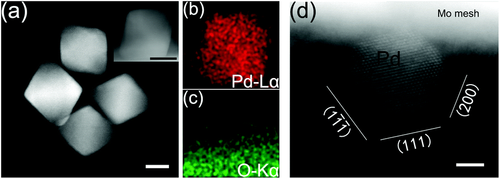 | ||
| Fig. 1 (a) HAADF–STEM characterization of the plasma cleaned octahedral Pd nanocrystal, the inset was the HAADF image for EDS mapping and corresponded to the mapping area, the scale bars are 10 nm. (b) and (c) EDS mapping results, the signal of Pd-Lα and O-Kα, respectively. (d) HAADF–STEM characterization of the plasma cleaned spherical Pd nanoparticle, the scale bar is 2 nm. | ||
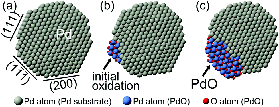
Fig. 2 shows the time sequenced TEM images for the surface oxidation of an octahedral Pd nanocrystal. The images are snapshots from the recording video (Movie S1, ESI†). HRTEM characterization of the same Pd nanocrystal is presented in the ESI (Fig. S2†), where a 3D schematics is shown together with the line profile analysis of the step edge region on the Pd(111) plane. The Pd nanocrystal was enclosed by the {100} and {111} facets, and the measured lattice fringes with a d-spacing of 0.223 nm, which corresponded to the {111} lattice planes of the face-centered cubic (fcc) structure Pd, were in accordance with the results in published papers (Table S3 and the cited references in the ESI†). The nanocrystal had many imperfect lattice planes on the rough surfaces, especially on the {111} surface. It was found that the lattice spacing of surface layers in the step edge region was much bigger than that of inner layers. The interplanar spacing between the topmost and the second topmost surface layers in the step edge region was 0.29 nm; while the interplanar spacing of inner layers of Pd(111) planes was 0.22 nm (Fig. S2†). The closer to the surface, the greater the lattice spacing was.
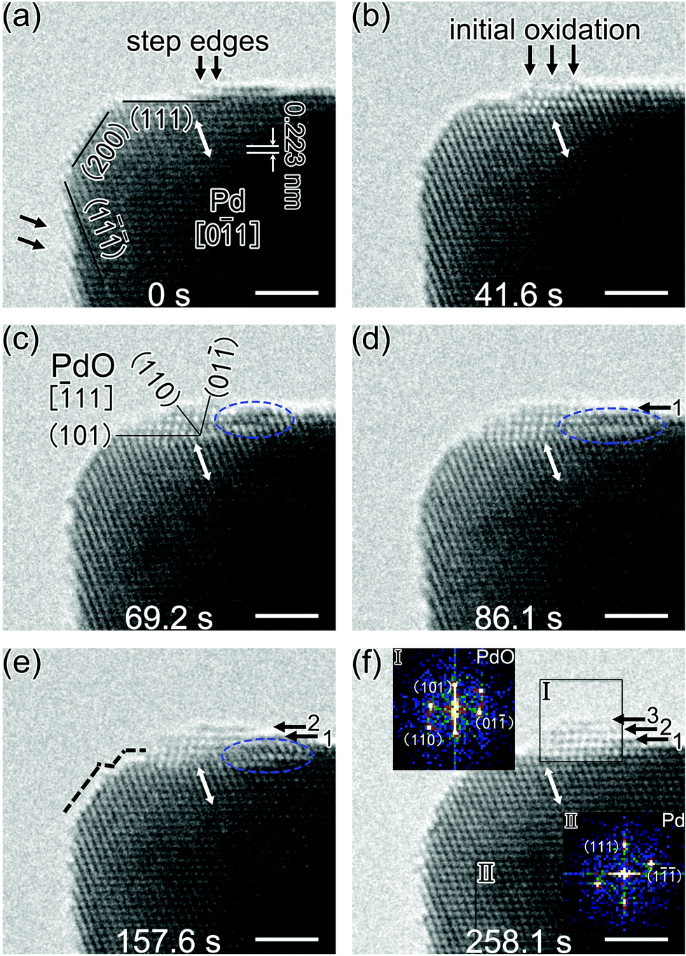 | ||
| Fig. 2 Time sequenced HRTEM images showing the in situ electron beam irradiation induced surface oxidation of octahedral Pd nanocrystal, (a) 0 s, (b) 41.6 s, (c) 69.2 s, (d) 86.1 s, (e) 157.6 s, and (f) 258.1 s. The oxidation initially started at the step edges on Pd(111) planes, then the oxide grew and PdO oxide layers was formed on the (111) surface, and finally the nanometer-sized oxide island was achieved. The insets in (f) are FFTs of the corresponding square areas. The scale bars are 2 nm. | ||
For the in situ electron irradiation experiments, the electron beam intensity was stabilized at 9.5 A cm−2; and the column pressure was controlled at 3.4 × 10⁻⁴ Pa, while the oxygen partial pressure was about 6.8 × 10⁻⁵ Pa. Fig. 2a shows the pristine surface structure of Pd nanocrystals based on the viewing direction of [0![[1 with combining macron]](https://www.rsc.org/images/entities/char_0031_0304.gif) 1]. Step edges standing on the Pd {111} surface are shown by the black arrows. Under an extended period of electron beam irradiation, the step edge region firstly started to change (Fig. 2b). After the reaction evolved further and the newly formed surface product grew bigger (Fig. 2c), the product was identified to be the tetragonal PdO phase, based on the coinciding lattice parameters (Table S4† lists out the commonly known palladium oxides and their corresponding lattice parameters). The PdO oxide phase (viewed in the [11] direction) and the Pd substrate phase appeared in an orientation of PdO(101)∥Pd(111). Accordingly, the Pd nanocrystal had initiated a surface oxidation reaction under the electron beam irradiation; the initial reaction in step edge regions served as the beginning of oxidation evolution. In the initial stage, since the newly formed oxide layers were only 1–2 monolayers, their structures were determined mainly by the interactions with the substrate and surface effects, and distinguished from either Pd or PdO.14 Reacting from the initial activated sites, the oxide on the nanocrystal surface had a fast rate growth on the Pd(111) surface. Due to the mismatch of two phases in lattice parameters, the PdO oxide phase had about 18% expansion compared to the Pd phase. An evident lateral growth of the surface oxide is shown in Fig. 2c and d. When the left side of the growing oxide met the nearest vertex corner of the nanocrystal, the growth stopped and the oxidation began to evolve towards right and vertical direction, and grew to be a nano-sized oxide island eventually (Fig. 2e and f). The insets in Fig. 2f show the Fast Fourier Transform (FFT) analyses of two phases. It clearly showed that the PdO oxide phase was formed on the nanocrystal surface, distinct from the metallic Pd phase. The bulk PdO formation was always accompanied by surface roughening. The white arrows in all six images marked the same Pd(1) planes, from which we could verify the lateral movements of the surface oxide. The vertical growth of the PdO oxide on the nanocrystal surface was marked by the numbered black arrows coplanar to the Pd(111) planes in Fig. 2d–f. The schematic structural model diagrams are given in Fig. 3. Considering the unknown oxygen adsorption sites, the illustration only focused on the edge-site oxidation process. The oxidation initially started in the step edge region; then, the oxide layers grew and the PdO oxide phase was formed on Pd(111) surfaces; and finally, a nanometer-sized oxide (PdO) island was achieved.
1]. Step edges standing on the Pd {111} surface are shown by the black arrows. Under an extended period of electron beam irradiation, the step edge region firstly started to change (Fig. 2b). After the reaction evolved further and the newly formed surface product grew bigger (Fig. 2c), the product was identified to be the tetragonal PdO phase, based on the coinciding lattice parameters (Table S4† lists out the commonly known palladium oxides and their corresponding lattice parameters). The PdO oxide phase (viewed in the [11] direction) and the Pd substrate phase appeared in an orientation of PdO(101)∥Pd(111). Accordingly, the Pd nanocrystal had initiated a surface oxidation reaction under the electron beam irradiation; the initial reaction in step edge regions served as the beginning of oxidation evolution. In the initial stage, since the newly formed oxide layers were only 1–2 monolayers, their structures were determined mainly by the interactions with the substrate and surface effects, and distinguished from either Pd or PdO.14 Reacting from the initial activated sites, the oxide on the nanocrystal surface had a fast rate growth on the Pd(111) surface. Due to the mismatch of two phases in lattice parameters, the PdO oxide phase had about 18% expansion compared to the Pd phase. An evident lateral growth of the surface oxide is shown in Fig. 2c and d. When the left side of the growing oxide met the nearest vertex corner of the nanocrystal, the growth stopped and the oxidation began to evolve towards right and vertical direction, and grew to be a nano-sized oxide island eventually (Fig. 2e and f). The insets in Fig. 2f show the Fast Fourier Transform (FFT) analyses of two phases. It clearly showed that the PdO oxide phase was formed on the nanocrystal surface, distinct from the metallic Pd phase. The bulk PdO formation was always accompanied by surface roughening. The white arrows in all six images marked the same Pd(1) planes, from which we could verify the lateral movements of the surface oxide. The vertical growth of the PdO oxide on the nanocrystal surface was marked by the numbered black arrows coplanar to the Pd(111) planes in Fig. 2d–f. The schematic structural model diagrams are given in Fig. 3. Considering the unknown oxygen adsorption sites, the illustration only focused on the edge-site oxidation process. The oxidation initially started in the step edge region; then, the oxide layers grew and the PdO oxide phase was formed on Pd(111) surfaces; and finally, a nanometer-sized oxide (PdO) island was achieved.
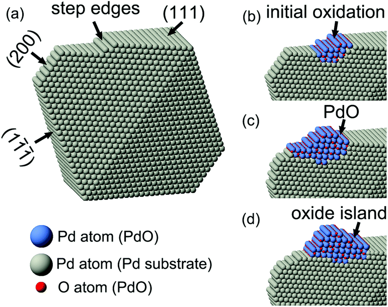 | ||
| Fig. 3 Pictorial illustration of the molecular structure models for the observed oxidation processes of octahedral Pd nanocrystal. The initial oxidation started at the step edges on Pd(111) planes, the PdO oxide layers then grew on the surface, and finally the oxide island was formed. | ||
Spherical Pd nanoparticles were also employed in our investigations to show that the beam induced surface oxidation of octahedral Pd nanocrystals was not an exceptional case. Sequential TEM images showing the structure evolution of a spherical Pd nanoparticle, which was also induced by electron irradiation, are presented in Fig. 4. TEM experiments were carried out using the same procedure as that of the octahedral Pd nanocrystals. Herein, the electron beam intensity was controlled at 3.3 A cm−2 by considering reaction rate control for a much smaller-sized Pd nanoparticle, and the column pressure was stabilized at 9.5 × 10⁻⁴ Pa, with an oxygen partial pressure of about 1.9 × 10⁻⁴ Pa. Fig. 4a shows the Mo mesh supported spherical Pd nanoparticle with a size of about 7 nm in diameter. It had a faceted structure. A few low-index planes were shown based on the viewing direction of [01]. The measured lattice fringes with a d-spacing of 0.224 nm corresponded to the Pd {111} planes. The initial reaction started from the vertex sites of Pd(111) and Pd(1) planes, highlighted by black arrows (Fig. 4b). With further irradiation, the reaction evolution spread from the vertex sites to the Pd(1) surface (Fig. 4c). But this spreading stopped at the other side of Pd(1) planes, marked by black triangles (Fig. 4c and d). In the following stage, the resultant began a three-dimensional growth on the Pd(1) surface (Fig. 4e). As shown in Fig. 4f, the reaction resultant was also confirmed to be PdO based on the interplanar spacing measurements. The d-spacings of 0.263 nm corresponded to the (101) and (10) planes of a tetragonal PdO, in the viewing direction of [00]; and the on-surface PdO oxide was found to be PdO(101)∥Pd(1). Schematic diagrams of the observed oxidation for the spherical Pd nanoparticles are drawn and shown in Fig. 5. The oxidation of faceted Pd nanoparticles started at the vertex sites and PdO oxide was formed on the Pd(1) surface eventually.
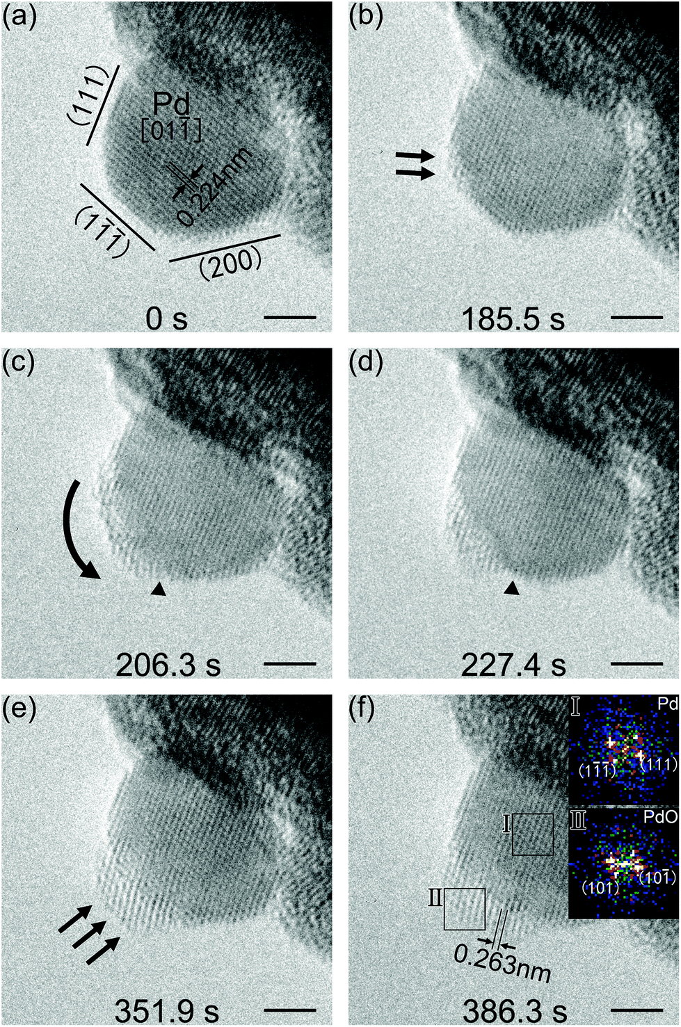 | ||
| Fig. 4 Sequential HRTEM images showing the in situ oxidation of a faceted Pd nanoparticle, (a) 0 s, (b) 185.5 s, (c) 206.3 s, (d) 227.4 s, (e) 351.9 s, and (f) 386.3 s. The oxidation started at the vertex of Pd(111) and Pd(1) planes, then evolved towards the Pd(1) surface, but stopped at the other side of Pd(1) planes. Continuously, the oxide began a three-dimensional growth on the Pd(1) surface and the PdO oxide was formed finally. The scale bars are 2 nm. | ||
 | ||
| Fig. 5 Schematic diagrams for the observed oxidation of a spherical Pd nanoparticle. The oxidation started from the vertex sites of Pd(111) and Pd(1) planes, and the PdO oxide was formed on the Pd(1) surface eventually. | ||
4 Discussions
We firstly discussed the effects of plasma cleaning for the adsorption and subsequent oxidation of Pd nanocrystals. The introduced oxygen would be plasma excited to form different types of radical species, such as O2+, O2−, O2*, O3, O, O+, O−, O*, etc., and some of them could further interact with the surface of nanocrystals, physically and/or chemically.43 For instance, Kim et al. confirmed the formation of an oxygen-enriched surface on the surface of Pt.44 As per our studies, the oxygen adsorption and atom/ion implantation might occur during the plasma treatment and cause weak oxidation on the outermost layers. For the octahedral Pd nanocrystal, we had observed an expansion of about 32% in the outermost layer in the step edge region standing on the Pd(111) surface (Fig. S2†) which was likely exacerbated by the plasma bombardment, and/or the knock-on damage of energetic electrons during TEM imaging. Nevertheless, the adsorption of oxygen onto the Pd surface was reported to be a spontaneous process.22,45 Due to the limitation of our TEM, we were not able to capture the adsorbed oxygen molecules on the surface of Pd nanocrystals.Back to the oxidation evolution, the energetic electron beam and the oxidation mechanism were much relevant. For Pd nanocrystals loaded on the same Mo grid, no obvious oxidation was observed in the absence of the electron beam. Also no palladium oxide was found on the surface before the TEM observations (just after plasma cleaning). Thus, it was concluded that electron irradiation was essential for the oxidation of Pd nanocrystals in this work. Independent experiments were also carried out to verify the effect of residual oxygen inside the TEM chamber, in which we filled the microscope column with pure N2 and kept other experimental parameters (beam dose, electron energy etc.) unchanged. Again, no oxidation of Pd nanocrystals occurred in the N2 enriched environment (Fig. S6†). This helped us to confirm the major contribution of oxygen coming from the residual gases inside the microscope chamber, not from the possible oxide layer on the Mo mesh via surface migration. Since oxidation reactions required a supply of atomic oxygen, together with sufficient mobility of metal atoms on the surfaces, we estimated the effects of electron beam irradiation. A temperature rise on the nanocrystals was expected to occur as a result of electron beam heating, which was proportional to the energy loss of the electron beam.46 The temperature rise was calculated, but due to the excellent thermal conductivity of Pd and Mo, it was less than 1 K and nearly negligible (details for the estimation of beam heating can be found in the ESI†). So, the oxidation was more likely activated non-thermally. As the beam induced oxidations were performed under the irradiation of high energy electrons, the electrons might activate the oxidation reactions directly. In general, two types of electron beam effects were considered in the TEM: knock-on damage and radiolysis. Note that the sputtering and/or beam induced migration of the atoms around the vertex sites was found under an extended period of beam irradiation (Fig. S6†). The interaction between electrons and gas molecules could also lead to the ionization of gas molecules, and the formation of radical species like atomic oxygen, thus promoting the oxidation of nanocrystals.36,47 Herein, it was inferred that after the dissociation of residual oxygen in our microscope column and the adsorbed oxygen on Pd surfaces by the high energy electrons, the atomic oxygen adsorbed on Pd surfaces, further leading to subsequent oxidation.
Regarding the detailed oxidation kinetics, previous studies on the surface oxidation of Pd(111) suggested a two-step process of oxygen adsorption and diffusion at room temperature,23 while the bulk PdO would further form at elevated temperatures.23,24 The oxidation began with oxygen adsorption. During the adsorption, oxygen preferred to bind with surface defects,23,48,49e.g. step edges and vertex sites, due to their unsaturated bonds and high surface energy. Also, we found that the oxidation only occurred on the surface steps of Pd(111) on octahedral Pd nanocrystals as shown in Fig. 2. This position selectivity might be related to the uneven thickness of Pd(111) steps along the beam direction, meaning that thinner Pd(111) sites had a larger ratio of low-coordinated atoms, which were more competitive to form PdO nucleate sites for continuous crystal growth. The oxygen adsorption and incorporation onto the subsurface in the step edge region or vertexes would also make these sites less stable due to the additional cost of distorting the substrate lattice and breaking metal bonds.50 Such defects were well-suited as nucleation centers. Moreover, these sites provided an easier diffusion path for oxygen. Hence, the step edge region with the lattice expansion or the vertex sites initially served as activated sites and nucleation centers for the oxidation of Pd nanocrystals or nanoparticles, respectively. Accordingly, with the initial oxidation sites like step edges or vertex sites, in a low oxygen partial pressure system (10−5 Pa), the oxidation evolution of Pd nanocrystals eventually formed nanometer-sized PdO oxide islands on Pd {111} surfaces.
It was suggested that the precursor state distinct from PdO or meta-stable surface oxides could occur during the Pd(111) oxidation.24,30,31,51 While in this work, despite the ultrathin resultant oxide layers (only 1–2 monolayers) at the initial oxidation stage, whose stoichiometry could not be determined precisely via HRTEM image analysis, only the formation of PdO was observed. The Pd–Pd nearest neighbour distance is 0.305 nm in PdO vs. 0.275 nm in Pd, the oxidation thus requires expansion of the Pd surface. One way for this surface relaxation was through surface reconstruction, e.g. by ejecting Pd atoms outwards. The blue dashed circles had marked the abnormal contrast regions (Fig. 2c–e). On the other hand, at the vertex corner of the octahedral Pd nanocrystal, small nanoscale steps were formed, as pointed by the black dashed lines (Fig. 2e). It revealed a diffusion of surface metal atoms during the oxidation reaction. Hence, both rearranging bulk atoms and the diffusion of the corner/surface atoms supplied the metal atoms needed for the oxide island growth.
The octahedral Pd nanocrystal and spherical Pd nanoparticle displayed similar surface oxidation evolution. However, the reaction rate and the oxidation degree presented here were of great difference. At 157.6 s, the oxidation of octahedral Pd nanocrystals had evolved in about six surface layers; while at 185.5 s, the vertex sites of spherical Pd nanoparticles just began to evolve. After this, the oxidation of spherical Pd nanoparticles had a great extent of oxide formation with about 20.6% area ratio at 386.3 s, compared to the 1.3% area ratio of surface oxide (still six layers) on octahedral Pd nanocrystals (Table S1†), as estimated from their projected areas. This distinction of the reaction rate was mainly concerned with the particle size, the electron beam intensity, and the oxygen partial pressures that we provided (Fig. S3–S5,† more cases of irradiation oxidation on spherical Pd nanoparticles; Tables S1 and S2†). In this work, in spite of the limited samplings, we could still find that smaller sized Pd nanoparticles reacted more rapidly, which might be owing to their higher surface energy. For the spherical Pd nanoparticles (Fig. 3/Movie S2, Fig. S3/Movie S3, and Fig. S4†), the oxide growth was preferential on the Pd {111} surface. On one hand, the {100} facets had a stronger capability of generating active oxygen species than the {111} facets, but molecular O2 was more active on the Pd(100) crystal surface than on Pd(111),22 in other words it was more difficult to dissociate an oxygen molecule on Pd(111). On the other hand, it was found that O atoms were adsorbed on the bridge site on Pd(100) and the fcc site on the Pd(111) surface, and O atoms had much higher adsorption energies on Pd(100) (−4.70 eV) than on the Pd(111) (−4.49 eV) surface.52 The irradiation of high energy electrons not only decomposed oxygen molecules into atomic oxygen promoting the oxidation as mentioned above, but could also desorb oxygen from the metal/metal oxide surfaces due to the knock-on effect and surface sputtering. The balance of the competing effects depended on the partial pressure of gases, the electron current density and the orientation of surfaces with respect to the electron beam.36 Herein, the {111} surface was likely to have higher oxygen coverage under the provided experimental conditions, thus a preferential oxide growth on Pd {111} surfaces was observed on spherical Pd nanoparticles. It would be interesting to control these factors, like oxygen pressure, electron beam intensity and temperature, to identify their contributions. Although here we used an electron beam to decompose O2 and activated the oxidation, the ion diffusion and oxidation features, like the initial reaction at step edges or vertex sites, and the crystallography preference, could offer guidance for understanding the oxidation mechanisms of metals at the nanoscale, especially at low oxygen pressure and low temperature involved oxidation reactions.
5 Conclusions
In summary, we have presented an in situ study on the surface oxidation behaviour of Pd nanocrystals induced by electron beam irradiation using two types of Pd nanocrystals, as octahedral and spherical structures. Valuable insights into the surface oxidation process and surface diffusion are obtained. The observations at the atomic scale showed that the oxidation preferred to launch reactions at the active sites, like the step edges or the vertex sites. The faceted spherical Pd nanoparticles showed a crystallography preference for the surface oxidation, which was on the Pd {111} surface. Both Pd nanocrystals were oxidized and formed nanometer-sized PdO oxide islands. The electron beam in the microscope had promoted the oxidation on Pd nanocrystals. The oxidation layer thickness and/or the island size depend on the oxygen partial pressure in the column, the irradiation time and the e-beam dose on the samples.Acknowledgements
This work was financially supported by the National Natural Science Foundation of China (Grant No. 11227403, 51472215, 51222202 and 91545113), and the Cyrus Tang Center for Sensor Materials and Applications. The work in the UK was supported by Engineering and Physical Sciences Research Council (Grant No. EP/G070326/1). Z. Y. Li thanks the Qiushi Foundation for a visiting Chair Professorship in ZJU. The collaboration between UK and CN side was supported by the 111 project under grant No. B16042. This work made use of the resources of the Center of Electron Microscopy of Zhejiang University.Notes and references
- K. Zhou and Y. Li, Angew. Chem., Int. Ed., 2012, 51, 602–613 CrossRef CAS PubMed.
- J. Park, J. Joo, S. G. Kwon, Y. Jang and T. Hyeon, Angew. Chem., Int. Ed., 2007, 46, 4630–4660 CrossRef CAS PubMed.
- Y. Zhou, Z. Wang and C. Liu, Catal. Sci. Technol., 2015, 5, 69–81 CAS.
- W. Zang, G. Li, L. Wang and X. Zhang, Catal. Sci. Technol., 2015, 5, 2532–2553 CAS.
- Y. Han, Z. Y. He, S. L. Wang, W. Li and J. L. Zhang, Catal. Sci. Technol., 2015, 5, 2630–2639 CAS.
- B. L. Hendriksen and J. W. Frenken, Phys. Rev. Lett., 2002, 89, 046101 CrossRef CAS PubMed.
- H. Over, Y. D. Kim, A. P. Seitsonen, S. Wendt, E. Lundgren, M. Schmid, P. Varga, A. Morgante and G. Ertl, Science, 2000, 287, 1474–1476 CrossRef CAS PubMed.
- D. W. Goodman, C. H. F. Peden and M. S. Chen, Surf. Sci., 2007, 601, L124–L126 CrossRef CAS.
- M. Lyubovsky and L. Pfefferle, Catal. Today, 1999, 47, 29–44 CrossRef CAS.
- J. G. McCarty, Catal. Today, 1995, 26, 283–293 CrossRef CAS.
- M. Lyubovsky, L. Pfefferle, A. Datye, J. Bravo and T. Nelson, J. Catal., 1999, 187, 275–284 CrossRef CAS.
- M. Crespo-Quesada, A. Yarulin, M. Jin, Y. Xia and L. Kiwi-Minsker, J. Am. Chem. Soc., 2011, 133, 12787–12794 CrossRef CAS PubMed.
- E. Antolini, Energy Environ. Sci., 2009, 2, 915–931 CAS.
- D. Ciuparu, M. R. Lyubovsky, E. Altman, L. D. Pfefferle and A. Datye, Catal. Rev.: Sci. Eng., 2002, 44, 593–649 CAS.
- M. Jin, H. Liu, H. Zhang, Z. Xie, J. Liu and Y. Xia, Nano Res., 2010, 4, 83–91 CrossRef.
- Y. Piao, Y. Jang, M. Shokouhimehr, I. S. Lee and T. Hyeon, Small, 2007, 3, 255–260 CrossRef CAS PubMed.
- X. Zhang, H. Yin, J. Wang, L. Chang, Y. Gao, W. Liu and Z. Tang, Nanoscale, 2013, 5, 8392–8397 RSC.
- S. Cheong, J. D. Watt and R. D. Tilley, Nanoscale, 2010, 2, 2045–2053 RSC.
- R. Wang, H. He, L. C. Liu, H. X. Dai and Z. Zhao, Catal. Sci. Technol., 2012, 2, 575–580 CAS.
- B. L. Hendriksen, M. D. Ackermann, R. van Rijn, D. Stoltz, I. Popa, O. Balmes, A. Resta, D. Wermeille, R. Felici, S. Ferrer and J. W. Frenken, Nat. Chem., 2010, 2, 730–734 CrossRef CAS PubMed.
- M. S. Jin, H. Zhang, Z. X. Xie and Y. N. Xia, Energy Environ. Sci., 2012, 5, 6352–6357 CAS.
- R. Long, K. Mao, X. Ye, W. Yan, Y. Huang, J. Wang, Y. Fu, X. Wang, X. Wu, Y. Xie and Y. Xiong, J. Am. Chem. Soc., 2013, 135, 3200–3207 CrossRef CAS PubMed.
- E. H. Voogt, A. J. M. Mens, O. L. J. Gijzeman and J. W. Geus, Surf. Sci., 1997, 373, 210–220 CrossRef CAS.
- G. Zheng and E. I. Altman, Surf. Sci., 2000, 462, 151–168 CrossRef CAS.
- G. Zheng and E. I. Altman, Surf. Sci., 2002, 504, 253–270 CrossRef CAS.
- J. Han, D. Y. Zemlyanov and F. H. Ribeiro, Surf. Sci., 2006, 600, 2752–2761 CrossRef CAS.
- H. H. Kan, R. B. Shumbera and J. F. Weaver, Surf. Sci., 2008, 602, 1337–1346 CrossRef CAS.
- T. W. Orent and S. D. Bader, Surf. Sci., 1982, 115, 323–334 CrossRef CAS.
- F. P. Leisenberger, G. Koller, M. Sock, S. Surnev, M. G. Ramsey, F. P. Netzer, B. Klotzer and K. Hayek, Surf. Sci., 2000, 445, 380–393 CrossRef CAS.
- G. Ketteler, D. F. Ogletree, H. Bluhm, H. Liu, E. L. Hebenstreit and M. Salmeron, J. Am. Chem. Soc., 2005, 127, 18269–18273 CrossRef CAS PubMed.
- H. Gabasch, W. Unterberger, K. Hayek, B. Klötzer, E. Kleimenov, D. Teschner, S. Zafeiratos, M. Hävecker, A. Knop-Gericke, R. Schlögl, J. Han, F. H. Ribeiro, B. Aszalos-Kiss, T. Curtin and D. Zemlyanov, Surf. Sci., 2006, 600, 2980–2989 CrossRef CAS.
- M. K. Rose, A. Borg, J. C. Dunphy, T. Mitsui, D. F. Ogletree and M. Salmeron, Surf. Sci., 2003, 547, 162–170 CrossRef CAS.
- M. K. Rose, A. Borg, J. C. Dunphy, T. Mitsui, D. F. Ogletree and A. Salmeron, Surf. Sci., 2004, 561, 69–78 CrossRef CAS.
- H. Yoshida, Y. Kuwauchi, J. R. Jinschek, K. Sun, S. Tanaka, M. Kohyama, S. Shimada, M. Haruta and S. Takeda, Science, 2012, 335, 317–319 CrossRef CAS PubMed.
- T. Fujita, T. Tokunaga, L. Zhang, D. Li, L. Chen, S. Arai, Y. Yamamoto, A. Hirata, N. Tanaka, Y. Ding and M. Chen, Nano Lett., 2014, 14, 1172–1177 CrossRef CAS PubMed.
- H. Yoshida, H. Omote and S. Takeda, Nanoscale, 2014, 6, 13113–13118 RSC.
- X. Huang, T. Jones, H. Fan and M.-G. Willinger, Adv. Mater. Interfaces, 2016, 3, 1600751 CrossRef.
- Y. Jiang, G. Zhu, F. Lin, H. Zhang, C. Jin, J. Yuan, D. Yang and Z. Zhang, Nano Lett., 2014, 14, 3761–3765 CrossRef CAS PubMed.
- W. Yuan, Y. Wang, H. Li, H. Wu, Z. Zhang, A. Selloni and C. Sun, Nano Lett., 2016, 16, 132–137 CrossRef CAS PubMed.
- W. Liu, K. Sun and R. Wang, Nanoscale, 2013, 5, 5067–5072 RSC.
- X. Xiang, J. Nie, K. Sun, L. Zhang, W. Liu, J. Schwank, S. Wang, M. Zhong, F. Gao and X. Zu, Nanoscale, 2014, 6, 12898–12904 RSC.
- N. Zheng, J. Fan and G. D. Stucky, J. Am. Chem. Soc., 2006, 128, 6550–6551 CrossRef CAS PubMed.
- M. Mozetic, U. Cvelbar, M. K. Sunkara and S. Vaddiraju, Adv. Mater., 2005, 17, 2138–2142 CrossRef CAS.
- S. Y. Kim, K. Hong, K. Kim, H. K. Yu, W.-K. Kim and J.-L. Lee, J. Appl. Phys., 2008, 103, 076101 CrossRef.
- Z. X. Wang, X. F. Jia and R. Wang, J. Chem. Phys. A, 2004, 108, 5424–5430 CrossRef CAS.
- R. F. Egerton, P. Li and M. Malac, Micron, 2004, 35, 399–409 CrossRef CAS PubMed.
- J. B. Wagner, F. Cavalca, C. D. Damsgaard, L. D. Duchstein and T. W. Hansen, Micron, 2012, 43, 1169–1175 CrossRef CAS PubMed.
- M. Okada, L. Vattuone, M. Rocca and Y. Teraoka, J. Chem. Phys., 2012, 136, 094704 CrossRef PubMed.
- L. Li, L. Luo, J. Ciston, W. A. Saidi, E. A. Stach, J. C. Yang and G. Zhou, Phys. Rev. Lett., 2014, 113, 136104 CrossRef PubMed.
- M. Todorova, W. X. Li, M. V. Ganduglia-Pirovano, C. Stampfl, K. Reuter and M. Scheffler, Phys. Rev. Lett., 2002, 89, 096103 CrossRef CAS PubMed.
- J. Klikovits, E. Napetschnig, M. Schmid, N. Seriani, O. Dubay, G. Kresse and P. Varga, Phys. Rev. B: Condens. Matter, 2007, 76, 045405 CrossRef.
- C. Q. Lv, K. C. Ling and G. C. Wang, J. Chem. Phys., 2009, 131, 144704 CrossRef PubMed.
Footnote |
| † Electronic supplementary information (ESI) available. See DOI: 10.1039/c6nr08763a |
| This journal is © The Royal Society of Chemistry 2017 |