
Active magnetoplasmonic split-ring/ring nanoantennas†
Hua Yu
Feng
ab,
Feng
Luo
a,
Raul
Arenal
cd,
Luc
Henrard
e,
Fernando
García
b,
Gaspar
Armelles
*b and
Alfonso
Cebollada
b
aIMDEA Nanoscience, Faraday 9, Ciudad Universitaria de Cantoblanco, Madrid, 28049, Spain
bIMM-Instituto de Microelectrónica de Madrid (CNM-CSIC), Isaac Newton 8, PTM, Tres Cantos, Madrid 28760, Spain. E-mail: gaspar@imm.cnm.csic.es
cLaboratorio de Microscopias Avanzadas (LMA), Instituto de Nanociencia de Aragon (INA), Universidad de Zaragoza, C/ Mariano Esquillor, Zaragoza, 50018, Spain
dFundacion ARAID, Zaragoza, 50018, Spain
eDepartment of Physics & Research Group on Carbon Nanostructures (CARBONNAGe), University of Namur, 61 rue de Bruxelles, 5000 Namur, Belgium
First published on 17th November 2016
Abstract
Here we present a novel active system, which combines the plasmon resonance enhancement of the magneto-optical activity in magnetoplasmonic nanostructures and the strong electromagnetic field localization of split ring resonators. The structures consist of a gold split ring resonator placed on top of a gold nanoring in the section of which a Co nanodot is inserted. By placing the split ring gap on top of the nanodot, and continuously varying the split ring gap opening, we are able to tune and enhance the electromagnetic field intensity in the Co nanodot, as confirmed experimentally by EELS and numerically using DDA simulation methods. In this way we obtain structures with a magneto-optical activity, which is 3 times larger than that of equivalent magnetoplasmonic rings without a split ring on top. These enhanced performances are due to the better control of the positioning, dimensions, and shape of the different components of the system. Such improvements are achieved using hole-mask colloidal lithography technique combined with multiaxial evaporation of the different materials.
Introduction
The optical properties of matter can be controlled by the application of an external magnetic field via the magneto optical (MO) effect. At optical frequencies this effect is normally small, and several approaches have been proposed to increase the MO activity by, for example, using magneto-photonic crystals1,2 or more recently surface plasmon resonances (SPR).3,4 Plasmonic nanostructures allow confining light in subwavelength regions and producing a subsequent enhancement of the electromagnetic (EM) field at resonance. By nanostructure design and engineering of shape, dimensions, and spatial configuration, it is possible to modify the characteristic resonant modes of the system, and consequently control its EM field distribution and intensity.5 In this context, using localized SPR, large enhancements of the MO activity have been reported in a variety of structures.6–11 On the other hand, the alternative use of propagative surface plasmon modes12–14 or Bragg-related excitations15,16 has also led to an enhancement of the MO activity. All these different structures have been revealed as excellent platforms to incorporate plasmonic and MO functionalities, giving rise to the so called magnetoplasmonic systems, where both phenomena coexist and interact, and finding applications for example in sensing,17–19 integrated optics,20 and telecommunications.21–24 In this scenario, exploring innovative routes to further boost this already large MO effect in such systems will allow developing novel concepts and expanding the areas of application in this field.In general, the MO effect in the combined plasmonic and MO (usually ferromagnetic metals) systems is related to the EM field intensity in the MO components.3 However, due to the fact that the optical loss of the ferromagnetic metals is larger than that of the plasmonic noble metals,6 it is not straightforward to spatially localize the plasmon resonance induced EM field enhancement in the MO component. To overcome this limitation, here we propose a novel and strategic approach which represents a quantum leap in the already competitive MO performance of magnetoplasmonic systems by an additional increase, namely, more efficient confinement of the EM field in the MO active component. To do this, we incorporate in a magnetoplasmonic system an additional plasmonic element, which “forces” the EM field into the MO component and thus allows the extra enhancement. For this purpose we have selected a gold split ring nanoantenna, which is well known to produce, in resonance, large EM fields in its gap.25–30 This additional plasmonic element is combined with the iso-morphological magneto-plasmonic structure, a ring, which has previously shown plasmon enhanced MO activity with resonances in the visible and near infrared spectral range.11,31 By further optimizing the split ring gap opening, which is directly deposited on top of an Au ring with a Co nanodot under the split ring gap, a boost in the MO effect of a factor of 3 is obtained in the new structure with respect to the equivalent magnetoplasmonic ring. This result may find direct practical implications, for example by further extending the detection limits in already proposed ultrasensitive magnetoplasmonic gas- or bio-sensors, or increasing the figure of merit of magnetoplasmonic-based optical isolators and light modulators.
Experimental and numerical methods
Considering the fabrication of the proposed nanostructures, the stacking of several planar layers with different shapes (dot, ring, split ring) and accurate positioning on the nanoscale is really a challenge for the current top-down technology, such as electron-beam (E-beam) lithography.32 Therefore the novel bottom-up lithography method, the so-called hole-mask colloidal lithography (HCL)33,34 is chosen in the current work for the nanostructure fabrication, combined with multiaxial deposition under ultra-high vacuum, which allows precise control of the individual elements in their specific dimensions, shapes and relative positions.Typical HCL templates were fabricated on glass substrates as follows: a 200 nm PMMA resist layer was first spin-coated on the BK7 glass substrate, followed by the incubation of polystyrene (PS) spheres with 124 nm diameter with the PDDA polymer as an adhesive layer on the PMMA. Then, a 30 nm Au film was sputter-deposited over the whole template. Afterwards, the PS spheres were removed by tape-stripping, obtaining a perforated Au film mask on the PMMA layer. The unprotected PMMA was then etched away with oxygen plasma to allow enough space for the deposition of the structures under the Au film mask. As it can be estimated, in this way the HCL template is an easy-to-use, low-cost but large-area (over cm2) method and provides versatile control of the nanostructures to be fabricated.
The as-prepared templates were introduced through a load-lock into an ultra-high vacuum deposition chamber where Ti, Co, and SiO2 were deposited by electron beam evaporation, and Au was evaporated from an effusion cell. The multi-axial control of the sample holder in the chamber during the deposition allows the fabrication of complex shaped structures with different materials located at positions selected at will.35,36
After deposition, the template was eliminated by lift-off in acetone for 2 h in an ultrasonic bath, leaving the final structures on the glass substrates.
The structural morphology was characterized with both an atomic force microscope (AFM) and transmission electron microscope (TEM). The plane-view TEM sample was prepared by mechanical thinning from the back side with a dimple grinder to a thickness of ∼10 μm and then ion milling with low energy Ar+ ions. The ion beams were directed at a glancing angle onto the back side of the sample to minimize beam damage and preserve the surface volume of the film.
The optical response in the visible and near infrared range (400 nm–1500 nm) of the nanostructures was characterized with a spectroscopic ellipsometer (SE, M200Fi J. A. Woollam Co.™) in transmission mode. The magneto-optical (MO) activity was measured with a polar MO Kerr (p-MOKE) spectroscopy setup at 1.1 T magnetic field, which is described elsewhere.37 The purpose of the p-MOKE characterization with a static magnetic field is to show the maximum potential of our nanostructure with the saturated magnetization. However, it is easy to extend the static magnetic field to dynamic operation21 by simply alternating the magnetic field which will make our devices active.
To model and better understand the optical behaviour of the nanostructures, numerical simulations were performed using discrete dipole approximation (DDA) as implemented in the DDSCAT 7.3.0 software.38 The DDA method has been extensively used for the plasmonic response of nanoparticles. In brief, the optical responses of the nanoparticles are described by their bulk dielectric functions, assuming a discretization of the system by a set of dipoles on a cubic grid. The optical extinction is the sum of the total scattering and absorption cross section. The maps are generated with the Mayavi free software. The convergence with the number of dipoles (the discretization length) has been carefully checked. The distance between dipoles is 1.5 nm for all calculations and the total number of dipoles is ∼500![[thin space (1/6-em)]](https://www.rsc.org/images/entities/char_2009.gif) 000. Tabulated dielectric functions of Au39 and Co40 are used.
000. Tabulated dielectric functions of Au39 and Co40 are used.
Besides, for experimental confirmation of the electromagnetic field distribution around the nanostructure, spatially-resolved (SR) high-resolution electron energy loss spectroscopy (EELS) was performed. STEM-EELS data were obtained using a probe-corrected FEI Titan Low-Base 60–300 kV STEM instrument, operated at 80 kV and equipped with a Cs probe corrector, a high-brightness X-FEG gun, a monochromator and a Gatan Tridiem 866 ERS energy filter. Fifteen EEL spectra (of 30 ms each) were acquired for each probe position following a two-dimensional (2D) region across the nano-object. The convergence and collection angle were 25 and 35 mrad, respectively. Typical energy resolutions (full-width at half-maximum of the zero-loss peak (ZLP)) of the measurements were better than 250 meV. EEL spectra were acquired using the spectrum-imaging (SPIM) mode.41,42 After collecting the data, each EEL spectrum was aligned along the ZLP, whose tail was removed using a power law subtraction method.43,44
Results and discussion
The deposition process is schematically shown in Fig. 1(a) and the different structures considered in this work are shown in Fig. 1(b) and (c). First, the bottom Au rings (with a thin Ti ring layer underneath to improve adhesion to the substrate) are easily obtained by off-normal deposition (θ, polar angle) and continuous rotation of the substrate about its surface normal (φ, azimuthal angle). Thereafter, Co dots can be placed in specific locations on top of the Au rings (left in Fig. 1(a)) by selecting specific azimuthal angles (e.g. φ = 0° and 180° for dots at opposite positions on top of the Au bottom ring) at off-normal deposition. The remaining space between the Co dots can be filled by subsequent off-normal deposition of Au and continuous azimuthal oscillation of the substrate with the adequate angle spanning and deposition time (right in Fig. 1(a)). A final Au ring is deposited on top repeating the first off-normal, continuous azimuthal rotation step. Following this method, it is possible to select different configurations of Co nanostructures embedded in Au rings, such as continuous rings, opposite sectors or dots (Fig. 1(b)). This control on the structure can also be applied to the upper Au component, in order to deposit an Au split ring with the gap on top of a Co dot (Fig. 1(c)).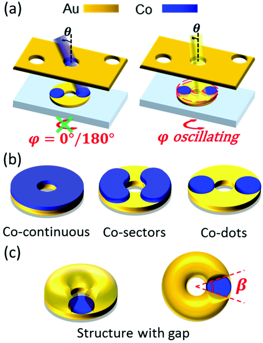 | ||
| Fig. 1 Schematics of the deposition process and of the different structures considered in this work. (a) Adequate control of the off-normal deposition angle (θ) and rotation angle (φ) about the surface normal allows obtaining a variety of structures. Left: Co dots at opposite positions on the bottom Au ring. Right: Gaps (dashed red contours) between the Co dots are filled with Au by azimuthal oscillation during the deposition. (b) Sketches of the intermediate states of the nanostructures with continuous Co rings, opposite Co sectors, and Co dots from left to right. (c) Sketches of structure with a tunable gap on top of a Co dot on a continuous bottom Au ring. β is the gap opening angle. | ||
Two series of structures were fabricated. First, in order to analyze the effect of redistributing the Co from a continuous Co ring towards a Co dot inclusion in an Au ring (Fig. 1(b)), a series of Au/Co/Au ring structures was grown in which the Co is distributed in the form of a continuous ring, two opposite sectors, two opposite dots and only one single dot. Then, the second series was based on the single Co dot structure, with Au split rings with gaps of different opening angles (β in Fig. 1(c)) on top of the Co dot. To avoid the possible oxidation of the exposed Co surface in the second case, the gaps in these split-ring/ring structures were filled with SiO2.
In Fig. 2 we show several representative AFM images of different structures fabricated in this way, including a collection of standard Au/Co/Au full rings (Fig. 2(a)), the intermediate state after the deposition of two Co dots on top of an Au ring (Fig. 2(b), corresponding to the last sketch in Fig. 1(b)), and a split-ring/ring structure with a 120° gap (Fig. 2(c), unfilled with SiO2). For this last type of structure, the profiles along a direction crossing the gap and the direction perpendicular are shown in Fig. 2(d). For both series, the relevant dimensions are: inner diameter: 60 nm; outer diameter: 300 nm; Ti adhesion ring thickness: 1–2 nm; bottom Au ring thickness: 7 nm; Co dot diameter: ∼120 nm, similar to the width of the ring; Co sectors span angle: 120°; Co dots/sectors/ring thickness: 5 nm for structures with two Co dots, Co sectors and Co ring, and 7 nm for structures with only one Co dot; top Au full ring and split ring thickness: ∼13 nm; split ring gap opening: β = 0°, 30°, 60°, 90°, 120°.
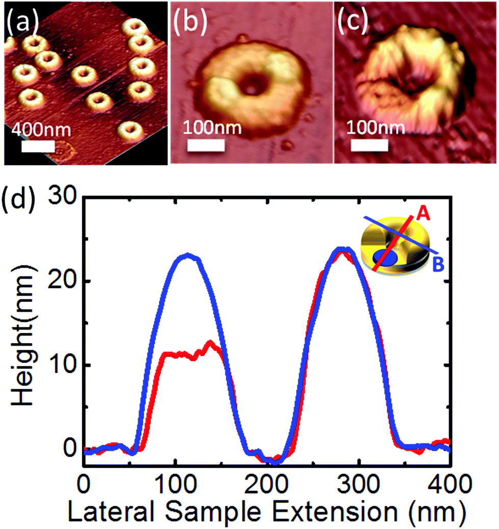 | ||
| Fig. 2 AFM images of (a) a complete Au/Co/Au trilayer ring structure, (b) intermediate stage in the fabrication process showing two Co dots on top of an Au ring and corresponding to the rightmost sketch in Fig. 1(b), (c) a gapped structure with a gap angle of β = 120°. After the ultimate covering process, all the structures have similar morphologies to that in (a) for structures without gap, or as in (c) for structures with gaps. (d) AFM profiles along (A direction in the inset, red line) and perpendicular to (B, blue line) the gap opening. Data are averaged from ten different structures of the same sample. Apart from the gap region, the contours show great similarity, implying the homogeneous deposition of the material and good reproducibility of the fabrication technique. | ||
We will first study the effect of redistributing Co in a full (Au ring)/(Co–Au ring)/(Au ring) structure on the optical resonances and MO activity. In Fig. 3(a), we show extinction spectra for two different light polarizations, parallel (continuous lines, x-polarization) and perpendicular (circles, y-polarization) to the direction along Co dots/sectors. Overall, the two high energy (HE) and low energy (LE) resonant modes typically observed in plasmonic nanorings11,31 are also visible here for both polarizations. As the amount of Co reduces from a continuous ring to a single dot, the extinction peak is becoming sharper, implying a smaller damping effect from the lossy Co component.6 In particular, a clear optical anisotropy in the LE peak is found for the sectors, dots and single dot structures. Moreover, for the sector and dot structures the spectral position of the LE peak for the x-polarized light is located at a higher energy than that for the y-polarized light. All these behaviors are very well reproduced qualitatively in the theoretically simulated extinction spectra (Fig. 3(b)), although the spectral positions of the plasmonic modes appear blue-shifted and the HE peak intensity is smaller with respect to the experimental spectra due to the different environments considered in the simulations (the Ti adhesive film and the SiO2 in the gap are not considered in the simulations). The optical anisotropy can be understood with the inhomogeneous in-plane EM field distribution at the plasmonic resonance induced by the Co compositions (Fig. S1†).
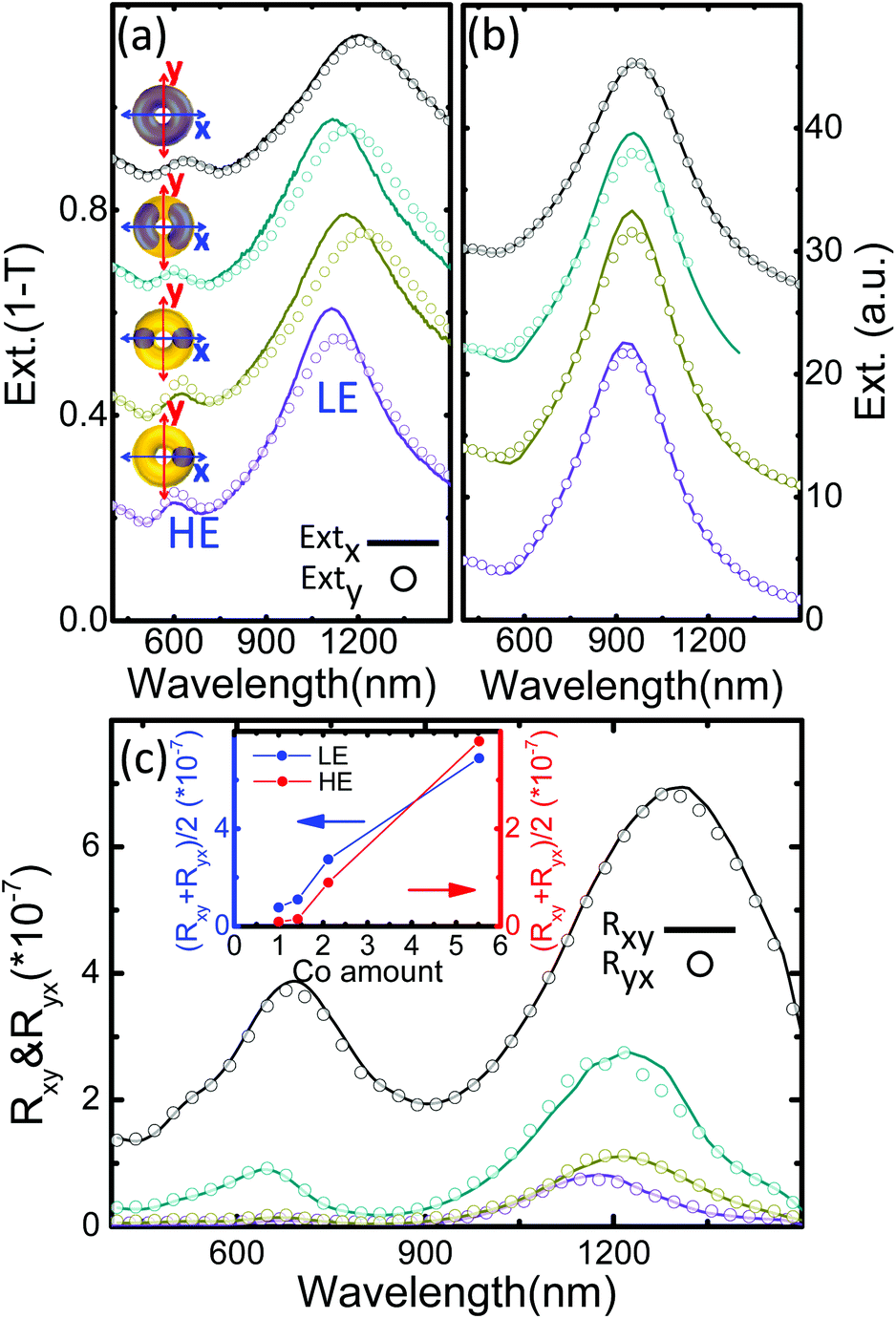 | ||
| Fig. 3 Optical and magneto-optical response for the series of full ring structures with varied Co inclusions (from Co dot to Co full ring). Experimental (a) and simulated (b) optical extinction for light polarizations along the dot/sector axis (x-polarization, solid lines) and perpendicular to this axis (y-polarization, circles). Spectra in (a) are shifted upwards for better clarity by 0, 0.2, 0.45, and 0.6 from Co dot to Co full ring, respectively. Spectra in (b) are also shifted upwards differently. Two plasmon modes in the low energy (LE) and high energy (HE) ranges are clearly observed for all the structures. The inclusion of the Co causes the optical anisotropy in them. (c) Pure magneto-optical components (Rxy and Ryx) for the same structures and light polarizations. Note here these spectra are not shifted upwards. Inset: averaged pure magneto-optical components ((Rxy + Ryx)/2) for HE and LE modes as a function of the amount of Co normalized to the Co dot sample (1 stands for 1 Co dot). The MO effect shows a strong dependence on the Co amount. | ||
The variation of the Co amount and shape in such structures also results in the evolution of the MO effects. The measurable values in the polar MO Kerr effect are the Kerr rotation θx,y and ellipticity εx,y, which are related to the Fresnel coefficients of the reflectivity matrix 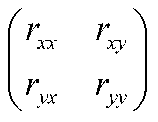 as follows:
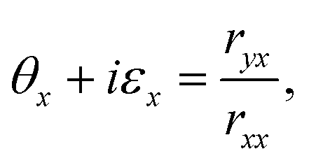
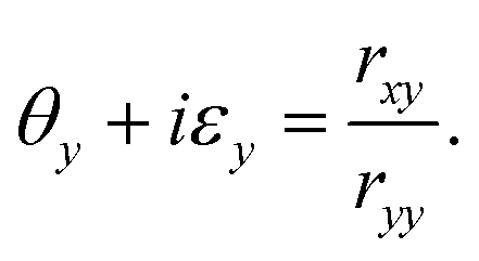 | (1) |
The modulus of the measured complex Kerr rotation is defined as the magneto-optical activity (MOA), expressed as
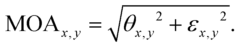 | (2) |
The MOA for this series of structures is shown in Fig. S2 in the ESI.† For convenience, we extract the pure MO contribution (polarization conversion) of the structures, Rxy and Ryx, as shown in Fig. 3(c), according to eqn (1) and (2), which are the squared moduli of the off-diagonal elements of the reflectivity matrix 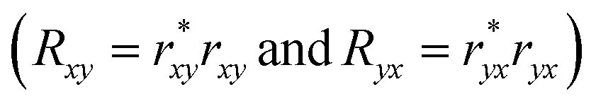 . Two peaks are observed and located in the spectral regions of the extinction peaks, implying the plasmonic resonance enhancement on the MO effects. The intensities of these two peaks increase as the structure evolves from one Co dot towards a complete Co ring. In the inset of Fig. 3(c), this evolution of the averaged peak magnitudes of Rxy and Ryx, as a function of the Co amount normalized to the individual Co dot is presented. As can be seen, a nearly linear increase of the pure MO response versus the amount of Co is observed, irrespective of the Co disposition within the structure.
Subsequently, we fix the amount of Co in the nanoring structure as a single Co dot, but a gap (or, in other words, a split ring nanoantenna) with a tunable angle is introduced on top of the Co dot. In Fig. 4, the results for these (Au split ring)/(Co dot in Au ring)/(Au ring) structures are shown. In the optical extinction spectra (Fig. 4(a)), the two HE and LE modes are observed for all the structures, the LE one being more intense. This LE mode exhibits a redshift as the gap opens up, especially when the light is polarized along the y-direction. Meanwhile, optical anisotropy is already present in the structure with 0° gap opening (no gap) as discussed above. Once the gap is introduced, the optical anisotropy is largely increased (from 0° gap to 30°). As the gap opens up, this optical anisotropy is being even larger. All these behaviours are qualitatively reproduced by the simulation (Fig. 4(b)). Again, due to the different environment considered in the theory the extinction peaks in the simulation appear blue-shifted with respect to the experimental ones. Obviously, the shift of LE modes and the increasing optical anisotropy as the gap opens up can be easily understood with the morphological modification of the gap and the subsequently induced redistribution of the EM field on the localized plasmon excitation (Fig. 5).
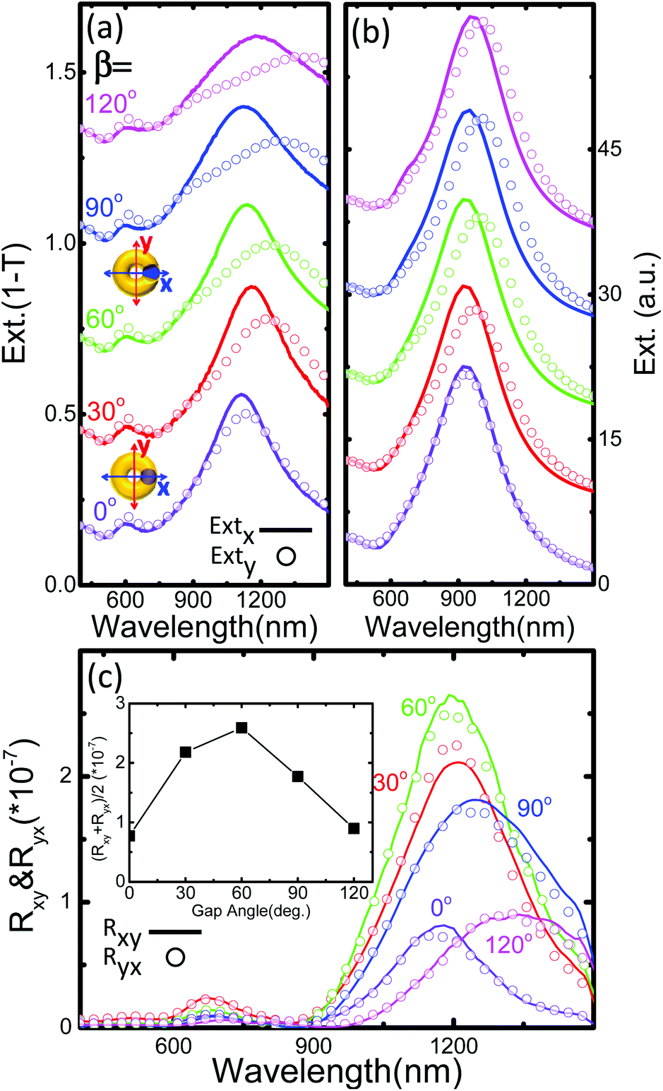 | ||
| Fig. 4 Optical and magneto-optical responses for the series of gapped structures with different gap openings and a single Co dot below the gap. Experimental (a) and simulated (b) optical extinction spectra for light polarizations along the dot/gap axis (x-polarization, solid lines) and perpendicular to this axis (y-polarization, circles). Spectra in (a) are shifted upwards for better clarity by −0.05, 0.15, 0.50, 0.85, and 1.15 from 0° to 120° gap sample, respectively. Spectra in (b) are also shifted upwards differently. The LE and HE plasmon modes are also available here, with an increasing optical anisotropy as the gap opens up. (c) Pure MO components Rxy and Ryx for the same structures and light polarizations. Inset: the Gap angle dependence of the averaged pure MO components ((Rxy + Ryx)/2) at LE peak positions. The MO effects in these samples are controlled dominantly by the gap angles, exhibiting a maximum for the structure with a 60° gap. | ||
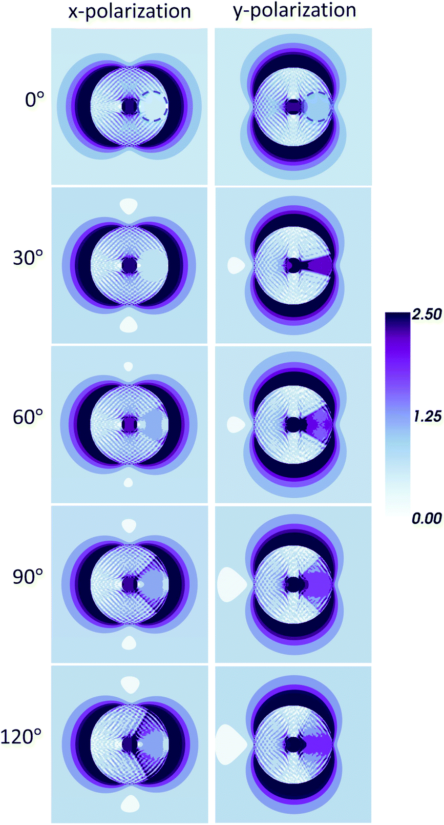 | ||
| Fig. 5 Electric field magnitude distribution in the central plane of Co dot for the gapped structures, corresponding to the LE extinction peaks in Fig. 4(b) obtained from the DDA simulations. For x- and y-polarized light, the Ex (left) and Ey (right) components are shown, respectively. The standing-wave-like distribution of the field is due to the discretization of the dipoles in the simulation method (the oscillation period is close to the discretization step). The dashed blue circles in the first row correspond to the position of the Co dot. Outside the structure, the field distribution shows a typical dipole character. Inside the structure, the field is more intense in the Au region for the structure without gap (0° gap). After the gap is introduced, the field is more intense in the Co region, especially for y-polarization, and is controlled by the gap angle. | ||
Due to the simple plasmon enhanced mechanism of the MO effect, two HE and LE peaks are observed in all the corresponding MO activities (Fig. S3 in the ESI†) as well as in the extracted pure MO effect, Rxy and Ryx (Fig. 4(c)) for all the structures. The redshift behaviour of the LE plasmonic modes as the gap opens up results in a redshift of the LE MO peaks. More importantly, the intensity of the LE MO peak shows a very strong dependence on the gap angle, exhibiting a maximum for an intermediate angle around 60°. This is clearly shown as an evolution in the inset of Fig. 4(c), where we present the averaged intensities of Rxy and Ryx at peak positions as a function of the gap angle. The maximum value at the intermediate angle (60°) exhibits an enhancement by a factor of 3 with respect to the 0° gap (no gap). A qualitatively similar behavior is also observed for the weaker HE mode. To further confirm this gap-enhanced MO effect, another structure with the Co dot in the opposite position to the gap region was fabricated (Fig. S4 in the ESI†), with a reduction in the MO activity by a factor of two.
The MO effect in such an Au/Co/Au nanostructure is related to the MO constant εMO,Co (off-diagonal elements in the dielectric tensor) of the Co material, as well as the field intensities Ex and Ey inside the Co region.12,45 Therefore, it is reasonable to assume that the observed behavior in the gapped structures, with a strong dependence of the MO effect on the gap angle is due to the efficient localization of the EM field in the Co dot. To confirm this assumption in Fig. 5 we present the electric field distributions in the central plane of the Co dot for all the gapped structures and both light polarizations. As it can be clearly seen, outside the nanostructure, the electric field distributions show the typical dipolar character. However, inside the ring, for x-polarization we observe a gradual increase of the intensity of the electric field inside the Co dot with the increasing gap angle. On the other hand, for y-polarization, the electric field in the Co exhibits maximum values for gap openings between 30° and 60°, being less intense for larger opening angles. This dependence on the gap opening angle for y-polarization is identical to that observed for the MO activity, therefore confirming the gap antenna effect as being responsible for the observed enhancement in the MOA.
This EM field localization in the Co dot area was further confirmed experimentally in this work by spatially-resolved (SR) high-resolution electron energy loss spectroscopy (EELS), which is a very powerful technique to experimentally obtain the in-plane electromagnetic field distribution at plasmon resonances.46,47 The SR-EELS analyses are performed on the (Au split ring)/(Co dot in Au ring)/(Au ring) structure with a 60° gap, which exhibits the maximum pure MO component. Fig. 6(a) displays the high-angle annular dark field (HAADF)-STEM micrograph of this nanostructure, in which the gap of the top Au split ring is clearly visible. In Fig. 6(b), we show the sum of the EELS spectra obtained from the area marked with the blue square (i) in Fig. 6(a), along with the unpolarized optical extinction spectrum measured for the same sample, using wavelengths as the horizontal axis for easier comparison. As can be seen, there is a remarkable similarity between the two spectra, with both HE and LE modes clearly observed in the EELS spectra, but with different relative intensities due to the different excitation mechanisms involved in the two measurements.46,48 Finally, the EEL signal map corresponding to the EM field intensity distribution of the LE mode is displayed in Fig. 6(c). There is a clear increase in the EM field in the region surrounding the split ring gap. We should clarify here that the map in Fig. 6(c) corresponds to the field distribution induced by the unpolarized light, therefore this field map can be considered as a combined Ex and Ey field distribution in Fig. 5 for the 60° gap structure. In this way, both the experiments and simulations confirm the presented argument for the physical mechanism of the further enhanced MOA by the introduction of a gap.
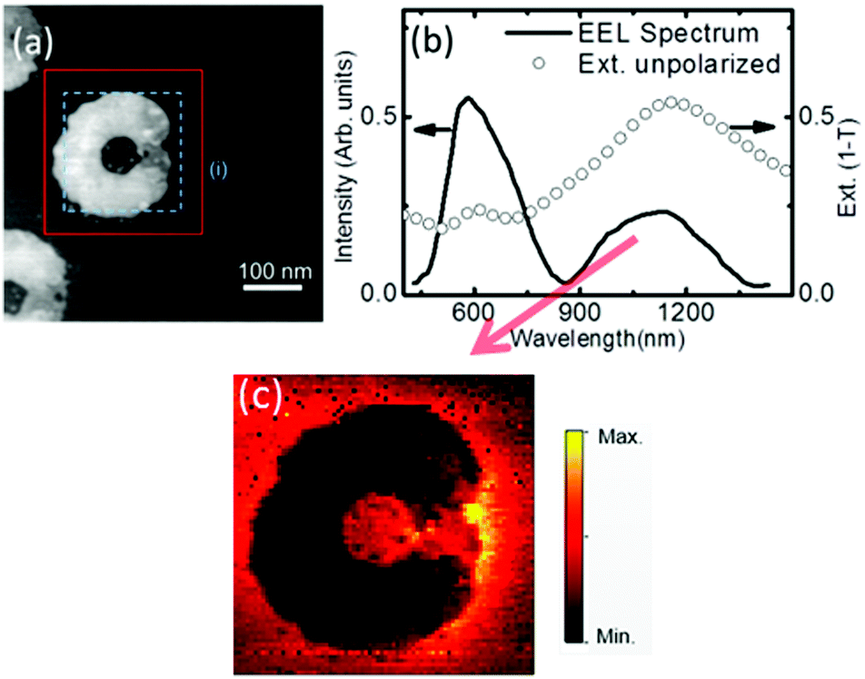 | ||
| Fig. 6 (a) HAADF-STEM image of a gapped nanostructure with a 60° gap angle, where the EELS SPIM (c) has been recorded in the area marked with red square. The gap region is clearly seen on the right side of the structure. (b) EEL spectrum, after background subtraction, corresponding to the sum of 400 spectra collected from the blue marked area (i) in (a), together with the extinction spectrum of the same sample for unpolarized light. The two spectra show very similar shapes with different relative intensities between LE and HE peaks. (c) The EEL intensity map showing the spatial distribution for the LE mode (red arrow) for this nanostructure. Remarkable enhancement is observed in the gap region, corresponding to the EM field enhancement in this region at the LE plasmon resonance. | ||
This result illustrates how, by combining magnetoplasmonic elements and plasmonic nanoantennas (split ring), it is possible to further confine and increase the EM field in specific locations, even in the regions with a larger optical loss. This way, the MOA of the whole structure can be greatly improved due to the further confinement of the EM field in the MO active material (Co), surpassing the already excellent performance of the initial magnetoplasmonic single element. Obviously further studies can be performed by increasing the complexity of the system, as for example by inserting a dielectric ring between the Au split ring and the magnetoplasmonic element, in order to explore even further EM field enhancements. In this case, parameters such as the separation between the Au split ring and the magnetoplasmonic ring, the gap opening, etc. must be explored in detail to determine the maximum MOA optimization that can be achieved. On the other hand, as a strategy, further enhancement of the EM field by the additional gap is not only suited for the applied structure model with only a Co dot inside. Very intuitively, as we show in the first series of structures with different shapes of Co inclusions where the MO effect is more related to the Co amount, further enhancement in the MO effect should be expected by opening a gap (or in other words, to generate a split ring nanoantenna) on top of one of the Co sectors or the Co continuous ring.
Conclusions
To summarize, in the current work we present a proof of concept, which demonstrates the strategic route to maximize the EM field in desired regions where MO-active elements with a higher optical loss are placed and yield outstanding results in terms of further enhanced MO activity. The complex structures studied in this work are realized, thanks to the developed hole-mask colloidal lithography (HCL) combined with multiaxial deposition techniques, which allows the accurate control of the component shape and position. A series of structures consisting of a split ring nanoantenna placed directly on top of a magnetoplasmonic ring element are fabricated and studied. An extra EM field localization is generated in the split ring gap, which “forces” the EM field to penetrate into the lossy Co nanodot in a more efficient way. In addition to the intrinsic plasmon enhanced MO activity of the magnetoplasmonic ring, the MO activity is further enhanced by this extra EM field localization. Furthermore, by considering different gap openings, a fine tuning and optimization of the extra EM field localization is obtained, resulting in a further increase of the pure MO effect by a factor of 3 with respect to the equivalent magnetoplasmonic ring without an additional split ring.The presented concept and the obtained boost in the MO activity may find rapid and direct practical implications, for example by further extending the detection limits in already proposed ultrasensitive magnetoplasmonic gas- or bio-sensing platforms, or increasing the figure of merit of magnetoplasmonic based optical isolators and light modulators. As a strategy, this proposed method by an additional plasmonic antenna to confine the EM field in a specific position, even in the region with a larger optical loss, can also find applications in the other areas related to the plasmon enhanced light–matter interactions, such as surface enhanced Raman spectroscopy,49 upconversion photoluminescence (PL),50etc., to obtain a further enhanced sensitivity or luminescence and improve their utilities. Moreover, since our nanoring structures exhibit the bimodal resonance behavior with the ratio of the resonant wavelengths very close to the factor of 2, it makes the structures ideal candidates for nonlinear plasmonics such as second harmonic generation (SHG), where the linear plasmonic field enhancement can be fully utilized. Indeed, when exciting at an infrared wavelength of 1300 nm (which matches the strongest resonance) the resulting optical second harmonic will be further enhanced by the second weaker resonance around 650 nm. By further optimization of the nanostructure morphology, this match in the wavelengths could be even improved. Taking into account the discussed double-resonant behavior of linear magneto-plasmonic signals, the potential application of these structures in nonlinear magnetoplasmonics should be stressed.51,52 The sensitivity of the linear extinction spectra to different light polarization makes these structures even more ideal candidates to study nonlinear magneto-optics in great detail.
Acknowledgements
We acknowledge funding from the Spanish Ministry of Economy and Competitiveness (CSD2008-00023, MAT2011-29194-C02-01, FIS2013-46159-C3-3-P, and MAT2014-58860-P), the EU 7th Framework Program (Grant Agreement 312483), and the EU-H2020 project (grant number 642742). H. Y. Feng acknowledges funding from CSC (Chinese Scholarship Council), grant no. 201206220112. F. Luo would like to acknowledge the support of NSFC (No. 51002003 & 11090332) as well as Ramon y Cajal grant RYC-2012-11954. The TEM measurements were performed in the Laboratorio de Microscopias Avanzadas (LMA) at the Instituto de Nanociencia de Aragon (INA) - Universidad de Zaragoza (Spain). This research used resources of the “Plateforme Technologique de Calcul Intensif (PTCI)” located at the University of Namur, Belgium, which is supported by the F.R.S.-FNRS under the convention no. 2.5020.11. The PTCI is the member of the “Consortium des Équipements de Calcul Intensif (CÉCI)”. R. A. gratefully acknowledges the support from the Government of Aragon and the European Social Fund under the project “Construyendo Europa desde Aragon” 2014–2020 (grant number E/26).References
- M. Inoue, R. Fujikawa, A. Baryshev, A. Khanikaev, P. B. Lim, H. Uchida, O. Aktsipetrov, A. Fedyanin, T. Murzina and A. Granovsky, J. Phys. D: Appl. Phys., 2006, 39, 151 CrossRef.
- M. Inoue, M. Levy and A. Baryshev, Magnetophotonics: From theory to applications, Springer, 2013 Search PubMed.
- G. Armelles, A. Cebollada, A. García-Martín and M. U. González, Adv. Opt. Mater., 2013, 1, 10 CrossRef; I. S. Maksymov, Rev. Phys., 2016, 1, 36 CrossRef.
- K. Lodewijks, N. Maccaferri, T. Pakizeh, R. K. Dumas, I. Zubritskaya, J. Åkerman, P. Vavassori and A. Dmitriev, Nano Lett., 2014, 14, 7207 CrossRef CAS PubMed.
- S. A. Maier, Plasmonics: Fundamentals and applications, Springer, New York, USA, 2007 Search PubMed.
- J. González-Díaz, A. García-Martín, J. M. García-Martín, A. Cebollada, G. Armelles, B. Sepúlveda, Y. Alaverdyan and M. Käll, Small, 2008, 4, 202 CrossRef PubMed; J. C. Banthí, D. Meneses-Rodríguez, F. García, M. U. González, A. García-Martín and G. Armelles, Adv. Mater., 2012, 24, OP36 Search PubMed.
- B. Toal, M. McMillen, A. Murphy, W. Hendren, M. Arredondo and R. Pollard, Nanoscale, 2014, 6, 12905 RSC.
- P. K. Jain, Y. Xiao, R. Walsworth and A. E. Cohen, Nano Lett., 2009, 9, 1644 CrossRef CAS PubMed.
- L. Wang, C. Clavero, Z. Huba, K. J. Carroll, E. E. Carpenter, D. Gu and R. A. Lukaszew, Nano Lett., 2011, 11, 1237 CrossRef CAS PubMed.
- V. Valev, A. Silhanek, W. Gillijns, Y. Jeyaram, H. Paddubrouskaya, A. Volodin, C. Biris, N. Panoiu, B. Clercq, M. Ameloot, O. Aktsipetrov, V. Moshchalkov and T. Verbiest, ACS Nano, 2011, 5, 91 CrossRef CAS PubMed.
- H. Y. Feng, F. Luo, R. Kekesi, D. Granados, D. Meneses-Rodríguez, J. García, A. García-Martín, G. Armelles and A. Cebollada, Adv. Opt. Mater., 2014, 2, 612 CrossRef CAS.
- C. Hermann, V. A. Kosobukin, G. Lampel, J. Peretti, V. I. Safarov and P. Bertrand, Phys. Rev. B: Condens. Matter, 2001, 64, 235422 CrossRef.
- V. I. Belotelov, I. A. Akimov, M. Pohl, V. A. Kotov, V. Kasture, D. R. Yakovlev, A. K. Zvezdin and M. Bayer, Nat. Nanotechnol., 2011, 6, 370 CrossRef CAS PubMed.
- J. Chin, T. Steinle, T. Wehlus, D. Dregely, T. Weiss, V. Belotelov, B. Stritzker and H. Giessen, Nat. Commun., 2013, 4, 1599 CrossRef PubMed.
- A. V. Chetvertukhin, A. A. Grunin, T. V. Dolgova, M. Inoue and A. Fedyanin, J. Appl. Phys., 2013, 113, 17A942 CrossRef.
- M. Kataja, T. Hakala, A. Julku, M. Huttunen, S. van Dijken and P. Törmä, Nat. Commun., 2015, 6, 7072 CrossRef CAS PubMed.
- B. Sepúlveda, A. Calle, L. M. Lechuga and G. Armelles, Opt. Lett., 2006, 31, 1085 CrossRef CAS; M. G. Manera, G. Montagna, E. Ferreiro-Vila, L. González-García, J. R. Sánchez-Valencia, A. R. González-Elipe, A. Cebollada, J. M. García-Martín, A. García-Martín, G. Armelles and R. Rella, J. Mater. Chem., 2011, 21, 16049 RSC.
- K. Kämpf, S. Kübler, F. W. Herberg and A. Ehresmann, J. Appl. Phys., 2012, 112, 034505 CrossRef.
- N. Maccaferri, K. E. Gregorczyk, T. V. A. G. de Oliveira, M. Kataja, S. van Dijken, Z. Pirzadeh, A. Dmitriev, J. Åkerman, M. Knez and P. Vavassori, Nat. Commun., 2015, 6, 6150 CrossRef CAS PubMed.
- D. Nikolova and A. J. Fisher, Phys. Rev. B: Condens. Matter, 2013, 88, 125136 CrossRef CAS; C. J. Firby and A. Y. Elezzabi, Optica, 2015, 2, 598 CrossRef; A. Davoyan and N. Engheta, Nat. Commun., 2014, 5, 5250 CrossRef PubMed; B. Spulveda, L. M. Lechuga and G. Armelles, J. Lightwave Technol., 2006, 24, 945 CrossRef.
- V. Temnov, G. Armelles, U. Woggon, D. Guzatov, A. Cebollada, A. Garcia-Martin, J. M. Garcia-Martin, T. Thomay, A. Leitenstorfer and R. Bratschitsch, Nat. Photonics, 2010, 4, 107 CrossRef CAS.
- V. Zayets, H. Saito, K. Ando and S. Yuasa, Materials, 2012, 5, 857 CrossRef CAS PubMed.
- H. Shimizu, Proc. SPIE, 2013, 8813, 88132C–1 CrossRef.
- D. Floess, J. Y. Chin, A. Kawatani, D. Dregely, H. U. Habermeier, T. Weiss and H. Giessen, Light: Sci. Appl., 2015, 4, e284 CrossRef CAS.
- Y. Lu, G. L. Liu, J. Kim, Y. X. Mejia and L. P. Lee, Nano Lett., 2005, 5, 119 CrossRef CAS PubMed.
- J. S. Shumaker-Parry, H. Rochholz and M. Kreiter, Adv. Mater., 2005, 17, 2131 CrossRef CAS.
- A. W. Clark, A. Glidle, D. R. Cumming and J. M. Cooper, J. Am. Chem. Soc., 2009, 131, 17615 CrossRef CAS PubMed; A. Clark and J. Cooper, Adv. Mater., 2010, 22, 4025 CrossRef PubMed.
- R. Jiang, F. Qin, Y. Liu, X. Ling, J. Guo, M. Tang, S. Cheng and J. Wang, Adv. Mater., 2016, 28, 6322 CrossRef CAS PubMed.
- P. Yu, S. Chen, J. Li, H. Cheng, Z. Li and J. Tian, Opt. Express, 2013, 21, 20611 CrossRef PubMed.
- Z. Tang and A. Wei, ACS Nano, 2012, 6, 998 CrossRef CAS PubMed.
- H. Y. Feng, F. Luo, D. Meneses-Rodríguez, G. Armelles and A. Cebollada, Appl. Phys. Lett., 2015, 106, 083105 CrossRef.
- N. Liu, H. Guo, L. Fu, S. Kaiser, H. Schweizer and H. Giessen, Nat. Mater., 2007, 7, 31 CrossRef PubMed.
- H. Fredriksson, Y. Alaverdyan, A. Dmitriev, C. Langhammer, D. Sutherland, M. Zäch and B. Kasemo, Adv. Mater., 2007, 19, 4297 CrossRef CAS.
- S. Cataldo, J. Zhao, F. Neubrech, B. Frank, P. Braun and H. Giessen, ACS Nano, 2011, 6, 979 CrossRef PubMed.
- J. Zhao, C. Zhang, P. Braun and H. Giessen, Adv. Mater., 2012, 24, OP247 CrossRef CAS PubMed.
- J. Zhao, B. Frank, F. Neubrech, C. Zhang, P. V. Braun and H. Giessen, Beilstein J. Nanotechnol., 2014, 5, 577 CrossRef PubMed.
- W. S. Kim, M. Aderholz and W. Kleemann, Meas. Sci. Technol., 1993, 4, 1275 CrossRef CAS.
- http://www.ddscat.org/ CrossRef CAS; B. T. Draine and P. J. Flatau, J. Opt. Soc. Am., 1994, 11, 1491 CrossRef CAS; P. J. Flatau and B. T. Draine, Opt. Express, 2012, 20, 1247 CrossRef PubMed.
- P. B. Johnson and R. W. Christy, Phys. Rev. B: Solid State, 1972, 6, 4370 CrossRef CAS.
- P. B. Johnson and R. W. Christy, Phys. Rev. B: Solid State, 1974, 9, 5056 CrossRef CAS.
- C. Jeanguillaume and C. Colliex, Ultramicroscopy, 1989, 28, 252 CrossRef.
- R. Arenal, F. De la Pena, O. Stephan, M. Walls, M. Tence, A. Loiseau and C. Colliex, Ultramicroscopy, 2008, 109, 32 CrossRef CAS PubMed.
- R. F. Egerton, Electron Energy-Loss Spectroscopy in the Electron Microscope, Plenum, New York, USA, 1996 Search PubMed.
- L. Francis, A. Mayoral and R. Arenal, Advanced Transmission Electron Microscopy: Applications to Nanomaterials, Springer, 2015 Search PubMed.
- D. Meneses-Rodríguez, E. Ferreiro-Vila, P. Prieto, J. Anguita, M. González, J. García-Martín, A. Cebollada, A. García-Martín and G. Armelles, Small, 2011, 7, 3317 CrossRef PubMed.
- M. Kociak and O. Stéphan, Chem. Soc. Rev., 2014, 43, 3865 RSC; M. Prieto, R. Arenal, L. Henrard, L. Gomez, V. Sebastian and M. Arruebo, J. Phys. Chem. C, 2014, 118, 28804 CrossRef CAS.
- R. Arenal, L. Henrard, L. Roiban, O. Ersen, J. Burgin and M. Treguer, J. Phys. Chem. C, 2014, 118, 25643 CrossRef CAS.
- F. J. Garcia de Abajo, Rev. Mod. Phys., 2010, 82, 209 CrossRef CAS.
- C. Haynes, A. McFarland and R. Duyne, Anal. Chem., 2005, 77, 338A CrossRef CAS.
- Y.-L. Wang, N. Estakhri, A. Johnson, H.-Y. Li, L.-X. Xu, Z. Zhang, A. Alù, Q.-Q. Wang and C.-K. Shih, Sci. Rep., 2015, 5, 1 CAS.
- I. Razdolski, D. Makarov, O. Schmidt, A. Kirilyuk, T. Rasing and V. Temnov, ACS Photonics, 2016, 3, 179 CrossRef CAS.
- V. Temnov, I. Razdolski, T. Pezeril, D. Makarov, D. Seletskiy, A. Melnikov and K. Nelson, J. Opt., 2016, 18, 093002 CrossRef.
Footnote |
| † Electronic supplementary information (ESI) available. See DOI: 10.1039/c6nr07864h |
| This journal is © The Royal Society of Chemistry 2017 |