
 Open Access Article
 This Open Access Article is licensed under a Creative Commons Attribution-Non Commercial 3.0 Unported Licence
Dry writing of highly conductive electrodes on papers by using silver nanoparticle–graphene hybrid pencils†
Jun-Ho
Park‡
,
Myung-Joo
Park‡
and
Jang-Sik
Lee
 *
*
Department of Materials Science and Engineering, Pohang University of Science and Technology (POSTECH), Pohang 37673, Korea. E-mail: jangsik@postech.ac.kr
First published on 2nd December 2016
Abstract
The development of paper electronics would enable realization of extremely cheap devices for portable, disposable, and environmentally-benign electronics. Here, we propose a simple dry-writing tool similar to a pencil, which can be used to draw electrically conducting lines on paper for use in paper-based electronic devices. The fabricated pencil is composed of silver nanoparticles decorated on graphene layers to construct layered hybrid nanostructures. This pencil can draw highly conductive lines that are flexible and foldable on conventional papers. Electrodes drawn using this pencil on conventional copy paper are stable during repetitive mechanical folding and highly resistant to moisture/chemicals. This pencil can draw a conductive line where its resistance can be tuned by changing the amount of nanoparticles. A nonvolatile memory device is realized on papers by hand written lines with different resistance. All memory elements are composed of carbons on papers, so complete data security can be achieved by burning the memory papers. This work will provide a new opportunity to fabricate electronic devices on real papers with good conductivity as well as robust mechanical/chemical stability.
Introduction
For many years, research on paper-based electronics has been actively conducted and its following development provides opportunities to realize lightweight, foldable, portable, low cost, and environmentally friendly devices.1 Owing to these beneficial characteristics of papers, lots of work have been introduced by adopting paper substrates for electronic devices such as transistors,2–6 RFID,7 solar cells,8,9 batteries,10,11 touch pads,12,13 antennas,14,15 sensors16,17 and also memory.18 To enable inexpensive, mass production at low temperatures many researchers have focused on solvent-based printing technologies.19–25 However, unlike other organic substrates paper is very permeable regardless of the solvent's polarity; consequently, the device properties can be degraded when the solvent wicks into the paper.22A pencil is a familiar writing tool that consists of a graphite-based solid core with a protective casing. Distinct from other writing implements that use inks to stain the paper, a pencil leaves a graphite layer on the paper surface by mechanical abrasion. It is possible because graphite has a 2-dimensional (2D) planar structure combined with weak van der Waals interactions, which can be separated layer-by-layer under smooth friction. Despite this characteristic, little attention has been paid to pencils as printing tools for the fabrication of paper devices.16,17,26,27 To our knowledge, there is no previous report on designing a pencil as a printing tool to draw conductive electrodes for the fabrication of paper-based electronic devices.
In this work we introduce a new dry printing method to draw conductive lines by simple ‘pencil-like’ mechanical drawing on paper. Printing silver nanoparticles (AgNPs) is a promising way to deposit metallic conductive lines due to their high conductivity and stability, but ‘pencil-like’ drawing on paper cannot be achieved using pure metal NPs on paper. The newly-designed pencil is composed of AgNPs decorated on graphene sheets to construct a layered nanostructure. Thus, conductive lines can be drawn on conventional papers by simple abrasion on paper, with graphene as the writing medium and AgNPs as the electrical current paths. Also, due to graphene's unique 2D network properties the resulting drawn line retains its conductivity after repeated folding, bending and exposure to various chemicals. Moreover, we posed the possibility of applying a facile dry writing method to fabricate an electronic device, especially a memory device. So far, research studies have been about graphene-based memory devices.28,29 But they need a complicated and difficult preparation process to fabricate the whole device. On the other hand, our device could be made by a simple method, hand writing. By adopting drawn conductive lines as electrodes and by modifying the quantity of silver to make the active layer of the memory device, it is found that the device can be operated successfully as a resistive switching nonvolatile memory device. It could be assumed that when an electric field is applied silver, which is known for being easily transportable inside an insulating layer,30,31 moves actively to construct a metallic filament inside the pencil trace. It is also tested to retain memory properties using several bending cycles to certify the effectiveness as a paper-based flexible electronic device.
Results and discussion
To construct a writable, conductive pencil material we develop a hybrid 2D structure that consists of reduced graphene oxide layers decorated with AgNPs which is a chemically-bonded structure. Fig. 1a shows a schematic synthesis procedure with microstructure design. Graphene oxide (GO) can be synthesized by using a modified Hummers’ method32 from the oxidation of pure graphite. This functionalized graphite was used because it can be easily exfoliated by simple ultrasonication, and its high surface hydrophilicity can induce thermodynamically favorable hetero-nucleation sites for adsorption and growth of AgNPs. We covered graphene surfaces with dense AgNPs which are sufficient to ensure that the drawn lines were electrically conductive. To realize this designed structure, we use a synthesis method based on a highly-concentrated AgNO3 solution, and use an organic reductant to slowly and efficiently reduce silver salts on the reduced GO (rGO) surfaces. After the centrifugation of the solution and drying to obtain powder, pressing is needed to fabricate a pencil-like pellet. The measured Vickers hardness of this pellet is ca. 0.85 HV. The SEM images of pure rGO (Fig. 1b) and AgNPs/rGO hybrid (Fig. 1c) powders show that the surface of the rGO was covered with high-density AgNPs. The proposed pencil can draw conductive lines on papers by simple handwriting (Fig. 1d). The inset shows a hand-writing process with a fabricated pellet. Friction-induced shear stress can break the inter-planar bonding in between graphene layers; the resulting separated sheets are dropped, pressed, and stuck on the paper surface. This conductive hybrid pencil can draw lines or write letters just as a conventional graphite-based pencil does. We drew lines on a commercially-available A4-size copy/print paper which has a rough and porous surface. We also measured the sheet resistance of the hybrid pencil trace and pure rGO of ca. 0.32 Ω □−1 and ca. 1.446 kΩ □−1, respectively. The big difference of the sheet resistance between the hybrid pencil and rGO is thought to be due to the contribution of AgNPs embedded in rGO layers.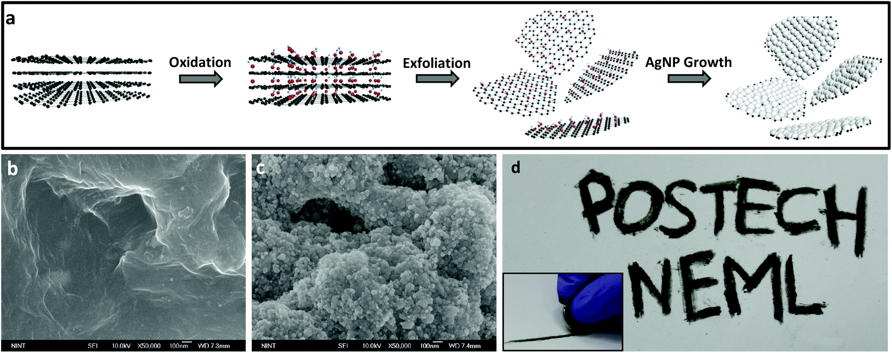 | ||
| Fig. 1 (a) Schematic images depicting the procedure of fabricating conductive AgNPs/rGO hybrid powder. SEM images of (b) pure rGO and (c) synthesized AgNPs/rGO hybrid powders. (d) Letters drawn with the AgNPs/rGO pellet. Inset shows a drawing process. | ||
As we draw a trace on paper with a fabricated hybrid AgNPs/rGO pencil, it could be depicted schematically (Fig. 2a) and this trace is composed of many layers of rGO and agglomerated AgNPs (Fig. 2b). In comparison to the conventional pencil trace, which consists of graphite, this hybrid structured pencil trace has a difference in the conduction path. In the case of graphite (Fig. 2c), there is only conduction through π–π bonding between carbons and the conduction between the upper and lower layers is nearly insulating because of the weak bonding of van der Waals forces. On the other hand, the AgNP/rGO composite has a connected structure between the rGO layers due to the bridging of AgNPs. Fig. 2d shows the schematic microstructure of this hybrid metal nanoparticle-embedded graphene layer. There are additional paths for electron transporting, which are the metallic path in silver nanoparticles and the junction path between graphene and silver nanoparticles. By using these paths electrons could be easily passed from one layer to the other layer so that it is possible to draw conductive lines with a low resistance.
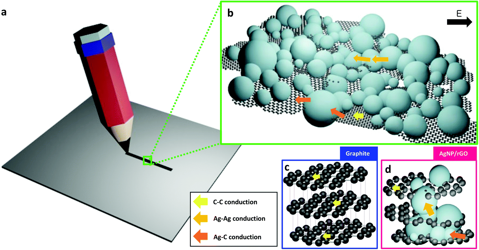 | ||
| Fig. 2 (a) Schematic images of a pencil-drawn line. (b) Schematic illustration describing a detailed conduction mechanism of the AgNPs/rGO-drawn trace. Three different colored arrows are to explain three different paths for electron transport. Electrical conduction of (c) graphite and (d) AgNPs/rGO could be compared. | ||
Simple handwriting can produce quite uniform, well-adhered lines on the surface of paper (Fig. 3a) even though it is bent or folded. This was observed at a higher resolution with scanning electron microscopy (SEM) and transmission electron microscopy (TEM). In Fig. 3b, the line maintained its adhesion to paper even after folding (Fig. 3c) verifying graphene's unique mechanical properties33 and metallic adhesive strength of AgNPs. A cross-sectional image was also obtained (Fig. 3d). To observe more accurately, a field-emission transmission electron microscope (FE-TEM) is used to show fully aggregated AgNPs on rGO sheets (Fig. 3e). TEM images provided the connected and aggregated chunk of AgNPs and this could contribute to the conduction process. EDS mapping was carried out to clearly separate rGO sheets from AgNPs (Fig. 3f). Green color represents carbon from rGO sheets and purple color represents AgNPs. High-resolution TEM images were also obtained to confirm that the AgNPs are attached to the rGO layer (Fig. 3g). The diffraction pattern of AgNPs featured a lattice parameter of 0.247 nm (Fig. 3h). Raman spectra are also obtained to clarify the modification of the chemical structure during the synthesis (ESI Fig. S1a†). There are two representative band shifts in graphite-related compounds, a D band and a G band.34,35 The two peaks are located at 1371 cm−1 and 1603 cm−1, each. The D band at 1371 cm−1 represents defects inside the graphite or graphene. When impurities or defects are present in the material, the sp3 bond of carbon atoms is vibrated so it draws a peak position at the D band. The G band is at 1603 cm−1 and it stands for the in-plane sp2 vibration in the material. The graphite sample has a very low ID/IG ratio which means that it has little defect inside. After it was oxidized to graphene oxide, lots of oxidation spots appeared and this led to an increase of ID/IG ratio. When it was reduced to rGO, oxidation sites would diminish. But the defects still persisted and increased during the reaction process so that the ID/IG ratio increased by about 10% compared to GO. Finally, the Raman spectrum of AgNP/rGO has a much higher intensity than that of rGO, which is due to surface-enhanced Raman scattering (SERS) which is originated from the intensified electromagnetic fields of AgNPs within the rGO. This high peak denotes that AgNPs are successfully synthesized within the rGO platelets.
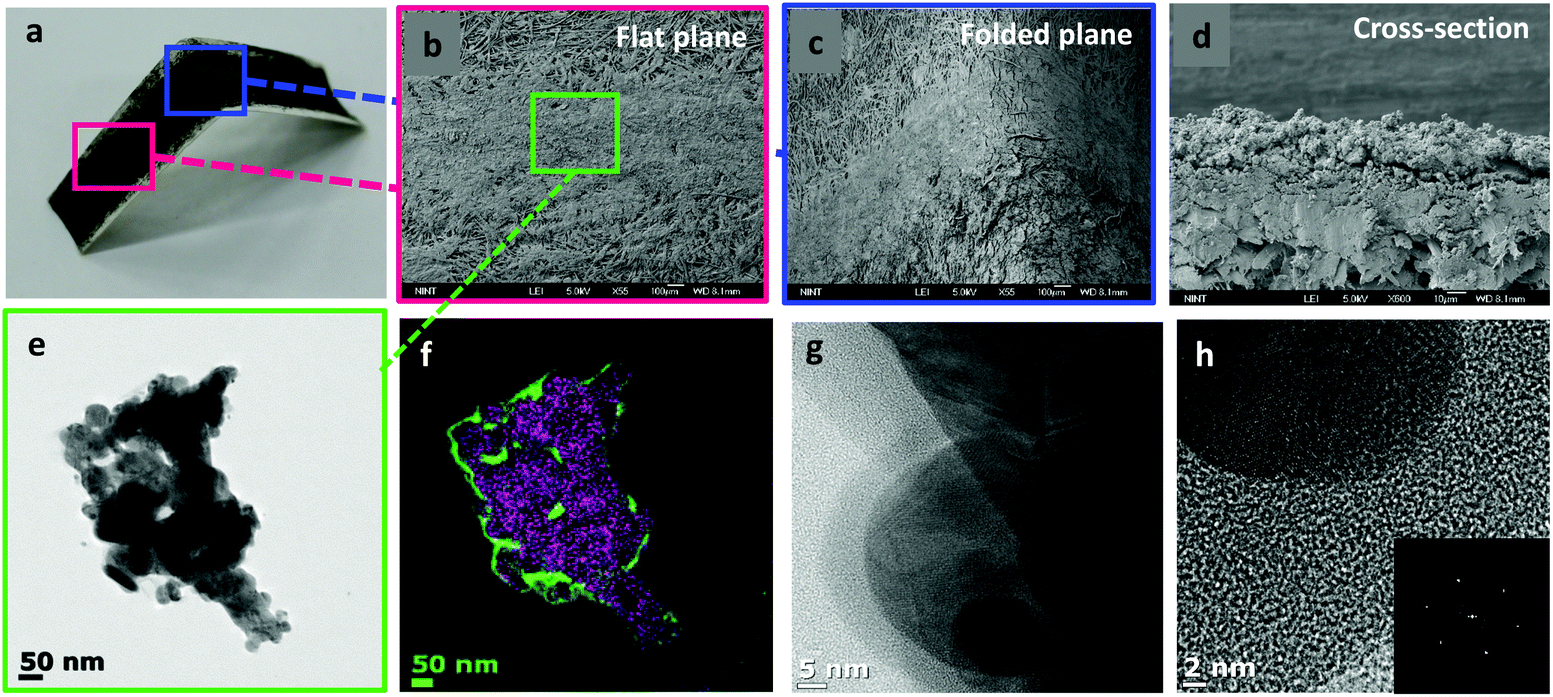 | ||
| Fig. 3 Images of the pencil track with various resolution. (a) The optical image of the 90° folded pencil trace and its SEM image at (b) a flat plane, (c) a folded plane and (d) a cross-sectional image of the drawn line. The pencil trace is also observed by TEM images. (e) Agglomerated silver nanoparticles on graphene sheets. For more clarity, (f) an EDS mapped image is obtained with distinctive color for silver and carbon atoms (green for carbon, purple for silver atoms). The HRTEM images of the AgNPs/rGO trace (g) with aggregated silver particles and (h) a single silver nanoparticle on graphene sheet with the diffraction pattern. | ||
For further application of pencil drawing on various electronic devices, its mechanical and chemical stability in a diverse environment should be confirmed. To improve the conductivity of the pencil-drawn line, the drawn lines were annealed after drawing. In this process, AgNPs are induced to aggregate and make stronger adherence in between the rGO layers. Due to the flexible nature of the paper substrate, the fabricated AgNPs/rGO electrode or device could be easily folded and bent. In Fig. 4a, resistance variance on different folded states (non-folded, 90° and 180° folded) is measured. Insets show a probing process of the pencil track with a multi-meter. There is a slight increase in resistance when folded, but it is still low enough for practical use. On several folding cycles the changes in resistance are recorded (Fig. 4b) and its value in the unfolded state was altered from 0.6 Ω to 1.4 Ω after 35 folding cycles. The inset shows a schematic view of unfolded and folded AgNPs/rGO electrodes. The resistance is almost recovered to its original value when the folded paper is open or unfolded. To prove its real time feasibility, we employed an oriental fan as an electrode with LED lights (Fig. 4c). We could freely draw an aesthetic illustration and Chinese letters on a fan composed of a paper. After attaching three LED lights and a pencil-drawn electrode, the fan was continually folded and unfolded. During several folding times, LED lights were consistently lightened. When the paper was merely bent (a radius of curvature of 5 mm) there was almost no change in resistance (Fig. S2†). Even when the line is folded, due to a unique mechanical property of graphene and AgNPs embedded stably on the folded graphene layer, it can provide a sufficient electrical pathway to conduct along the folded line.
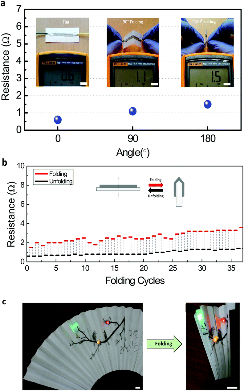 | ||
| Fig. 4 Electrical and mechanical properties of conductive lines drawn by a hand-written conductive pencil on papers. (a) Resistance measurement of the drawn conductive line (length of 4 cm and width of 3 mm) for unfolded, 90°-folded, and entirely-folded (180°) states. (b) Measured resistance data with multiple folding cycles. Both unfolded (black line), and folded (red line) resistances were measured with the number of folding cycles. (c) Pencil drawing art on a handheld folding fan. The optical images of electronic art on the paper folding fan; drawn oriental painting named ‘Mae-hwa’. Red, blue, and green LEDs emitted light with an attached battery in a, unfolded and b, folded states. The electrical current flows through the drawn conductive lines. | ||
These AgNPs/rGO electrodes are likely to be exposed to various wet spills in real life. Paper-based devices might not be economical if they are actually sensitive to chemicals/moisture and should be handled with great care. Electrodes introduced in this paper were reliable after soaking in various solvents including deionized (DI) water, ethanol, and toluene (Fig. 5a). Although the paper with the electrode was completely soaked in certain solvents (Fig. 5b), the electrical resistance was almost not changed for 6 h in both hydrophilic and hydrophobic solvents. This stable operation results from unique chemical properties of graphene, which ensure that the Ag/rGO structure has high chemical stability.36 To confirm the proper operation of conductive lines under wet conditions we drew a simple circuit that connected an LED and a 3 V battery, and then soaked the test circuit on paper in DI water. LED light is still on with a hybrid pencil drawn circuit after immersion in water (Fig. 5c). This result might verify the fact that the hybrid pencil-drawn circuit can endure an extreme condition such as being wet with water, ethanol and toluene. Also a long-term stability test under an ambient atmosphere (an average relative humidity of 62% and a temperature of 27 °C) was conducted to check its electrical properties for more than a month (Fig. S3†).
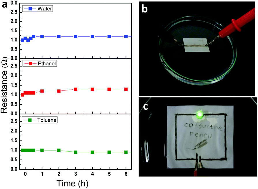 | ||
| Fig. 5 Stability of drawn conductive lines on copy paper under wet conditions. (a) Resistance change according to time under various chemical solvent wetting; in DI water (blue), ethanol (red), and toluene (green). (b) The optical image of the measured configuration. The paper with a drawn conductive line is completely soaked in water, ethanol, or toluene in the glass petri dish. (c) The optical image of LED lighting with a hybrid pencil drawn conductive line under water wetting. | ||
For further application of hybrid pencils to practical electronic device fabrication, we demonstrated pencil-drawn memory devices drawn with a hybrid AgNPs/rGO pencil (Fig. 6a–c). The whole process to produce a pencil-drawn memory device is just to draw three lines, two for electrodes and one for the resistive switching layer. The resistive switching layer is made with a pencil containing less AgNPs. I–V characteristics were measured under a dc voltage bias sweep (0 → −1.5 → 0 → 1.5 → 0) on the electrode (Fig. 6d). During 38 cycles, the device showed self-compliance and a quite clear set and reset process with a consistent on/off ratio of about 100 (Fig. 6e). Owing to its flexible nature, a paper-based electronic device can be operated under bent conditions. Finally, we ignited this paper-based memory to permanently eliminate the information stored in the device (Fig. S4†). It took 20 s for data to be totally removed after it was lit.
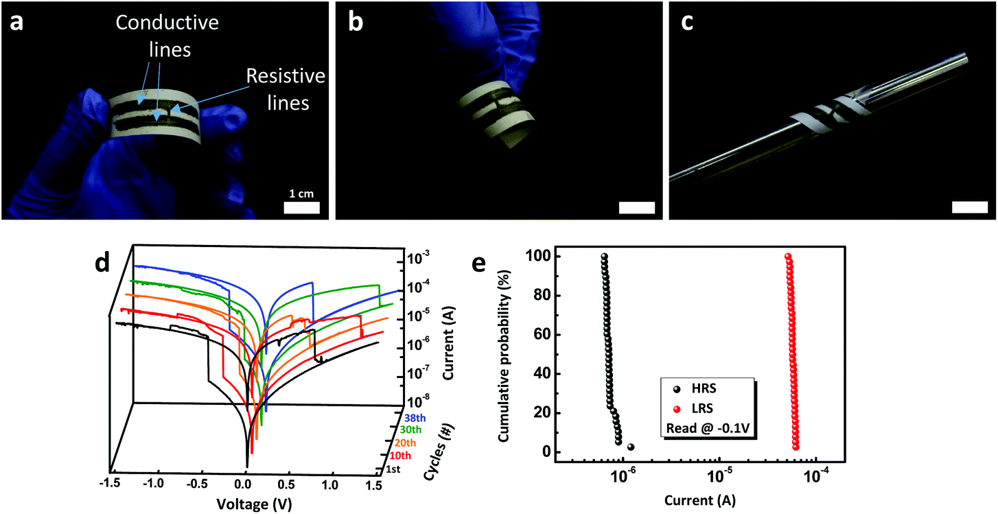 | ||
| Fig. 6 Resistive switching memory devices fabricated by pencil writing. (a–c) The optical images of pencil-drawn memory devices on papers (Scale bar: 1 cm). Memory devices are fabricated on papers, so folding, bending, or wrapping can be done. (d) I–V characteristics of the memory device on paper. (e) Cumulative probability of high resistance state (HRS) and low resistance state (LRS) current through 38 cycles. | ||
Conclusions
We have suggested a novel and facile method to fabricate electronic devices on papers by hand drawing using an AgNPs/rGO hybrid pencil. This pencil was fabricated by a solution synthesis process, which is composed of rGO layers with a high density of AgNPs. The pencil prints AgNPs/rGO hybrids; the AgNPs/rGO hybrid layer provides a conductive pathway and mechanical flexibility. This method of drawing electrical circuits has numerous advantages including dry-printability, simple process, high electrical conductivity, mechanical foldability, and chemical stability. This metal nanoparticle-based pencil drawing method as a new concept of printed electronics can be a viable technology to fabricate reliable electronic devices on papers. In this context, our fabrication of memory devices is an introductory remark on research about resistive switching memory devices which are made by hand, without using expensive and complicated equipment. In addition, devices can be fabricated on untreated, conventional papers with all components composed of carbons, so this will provide a new technology to fabricate devices for environmentally friendly products and manufacturing.Methods
Materials
All devices were fabricated using commercial copy/print papers (double A, 80 g m−2) without any treatment. Pure graphite powders (an average powder size of 30 μm) were purchased from Bay Carbon Inc. Diethanolamine (DEA) was purchased from Sigma Aldrich. Silver nitrate (AgNO3) powders (99.9% purity) were purchased from Kojima Chemicals. Ethyl alcohol (94.5% concentration), ethylene glycol (99.5% purity), sodium nitrate (99% purity), potassium permanganate (99.9% purity), and hydrochloric acid (35–37% concentration) were purchased from Samchun Chemicals. Toluene (99.5% purity), hydrogen peroxide (30% concentration) and sulfuric acid (95% concentration) were purchased from Daejung Chemicals. All materials were used without further purification.Synthesis of AgNPs/rGO hybrid nanocomposites
Graphene oxide (GO) powders were synthesized using a modified Hummers’ method as described previously.32 Nano-dispersed GO solution was prepared by mixing 0.27 g GO powder in 30 mL DI water with ultrasonication for 3 h. Then 18 g AgNO3 powder dispersed in 13.5 mL DI water was added to the exfoliated GO aqueous solution, and stirred for 2 h. To control the amount of silver inside the rGO layers, different amounts of silver nitrate were dissolved in the as-prepared solution; the solution for conductive electrodes contains 18 g of silver nitrate and the solution for resistive switching layers involves 9 g of silver nitrate. Then 40 mL DEA was injected while vigorously stirring. The reaction continued for 22 h to yield Ag-based nanocomposites. To remove the remaining DEA, the obtained colloidal solution was centrifuged at 8000 rpm for 20 min, three times; the used DI water was removed, the solutes were re-dispersed in new DI water, and repeatedly centrifuged each time. The resulting sediment was dried under ambient conditions to remove residual solvents. For comparison, pure rGO was prepared using the same method but without AgNO3.Fabrication of pencil pellet
The dried AgNPs/rGO powder was mixed with ethylene glycol to enhance the writing quality. Pellet-type pencils were fabricated by loading the prepared powder into a 20 mm-diameter cylindrical pellet die and compressing the powder by applying a 22 MPa force for a few seconds using a Hydraulic Press (Daejin Hydraulic Machinery Co., Ltd, THP 2A). To compare with a general graphite pencil, a pure graphite-based pellet was prepared using an analogous method.Pencil-drawn conductive lines
Conductive lines on paper were drawn using the pellet by physical abrasion with an applied force of 3–5 N measured using an analytical balance. A single drawing pass was sufficient to obtain pencil-like trace lines, but to obtain good conductivity several superimposed strokes were required. Drawn lines can be thermally annealed at elevated temperatures to improve the conductivity.Square circuit with LED light to test stability under wet conditions
To fabricate simple LED circuits on the paper, an 8 mm-diameter green LED and 3 V battery were attached using silver paste (Elcoat P-100, CANS) to a prepared pencil drawn circuit on paper. A square-shaped circuit with a dimension of 7 × 7 cm2 was drawn using the hybrid pencil pellet (Fig. 5c) before soaking in water. The paper was annealed at 150 °C for 3 h to optimize the device capability.Foldable electronic art
To fabricate an electronic foldable fan, 8 mm-diameter red, blue, and green LEDs were attached to a prepared oriental painting that had been drawn on a foldable fan. To prepare this conductive art painting on a handheld folding fan, we drew pencil painting on the copy paper first. The drawing was attached to the fan's wooden frame. The paper was annealed at 100 °C for 3 h.Fabrication of memory devices
To fabricate a resistive switching memory device with a pencil trace, two identical electrodes were drawn with a width of 3 mm. The gap between these electrodes is 3 mm. The 3 mm gap was used for subsequent resistive switching layer drawing. Each electrode was made with a pencil pellet containing 18 g of silver nitrate and 0.27 g of GO. A resistive switching layer was made with a pencil pellet with 9 g of silver nitrate and 0.27 g of GO.Characterization
Optical images were obtained using a digital camera. Microstructure images were obtained using field-emission scanning-electron microscopy (JSM-7401F, JEOL) and transmission-electron microscopy (JEM-2200FS, JOEL). Sheet resistance is measured using a four-point probe (2450 SourceMeter, Keithley). Mechanical folding tests were conducted by folding and unfolding a prepared conductive pencil line (length L = 40 mm, width W = 3 mm) drawn on paper connected with wires (Fig. 4a). The resistance changes were monitored using a multi-meter (Fluke-115). To analyze chemical stability the resistance of the drawn conductive lines using the hybrid pencil was measured after placing the test papers in glass petri dishes filled with DI water, ethanol, and toluene for 6 h (Fig. 5). Resistance under ambient conditions was measured daily for 35 days (Fig. S3†). The temperature, relative humidity, and resistance were recorded at the same time, every day. Raman shift spectra were obtained by using a Raman spectrometer (Ram II-Senterra, Bruker). Vickers hardness was measured using a Micro Vickers hardness tester (FM-700, Future Tech). Resistive switching properties of memory devices were investigated using a semiconductor parameter analyzer (4200-SCS, Keithley).Acknowledgements
This work was supported by the National Research Foundation of Korea (NRF-2016M3D1A1027663, NRF-2015R1A2A1A15055918). This work was also supported by the Future Semiconductor Device Technology Development Program (10045226) funded by the Ministry of Trade, Industry & Energy (MOTIE)/Korea Semiconductor Research Consortium (KSRC). In addition, this work was partially supported by the Brain Korea 21 PLUS project (Center for Creative Industrial Materials).References
- D. Tobjork and R. Osterbacka, Adv. Mater., 2011, 23, 1935–1961 CrossRef PubMed.
- D. H. Kim, Y. S. Kim, J. Wu, Z. J. Liu, J. Z. Song, H. S. Kim, Y. G. Y. Huang, K. C. Hwang and J. A. Rogers, Adv. Mater., 2009, 21, 3703–3707 CrossRef CAS.
- Y. Fujisaki, H. Koga, Y. Nakajima, M. Nakata, H. Tsuji, T. Yamamoto, T. Kurita, M. Nogi and N. Shimidzu, Adv. Funct. Mater., 2014, 24, 1657–1663 CrossRef CAS.
- G. Grau, R. Kitsomboonloha, S. L. Swisher, H. K. Kang and V. Subramanian, Adv. Funct. Mater., 2014, 24, 5067–5074 CrossRef CAS.
- S. Thiemann, S. J. Sachnov, F. Pettersson, R. Bollstrom, R. Osterbacka, P. Wasserscheid and J. Zaumseil, Adv. Funct. Mater., 2014, 24, 625–634 CrossRef CAS.
- U. Zschieschang and H. Klauk, Org. Electron., 2015, 25, 340–344 CrossRef CAS.
- V. Sanchez-Romaguera, S. Wunscher, B. M. Turki, R. Abbel, S. Barbosa, D. J. Tate, D. Oyeka, J. C. Batchelor, E. A. Parker, U. S. Schubert and S. G. Yeates, J. Mater. Chem. C, 2015, 3, 2132–2140 RSC.
- M. C. Barr, J. A. Rowehl, R. R. Lunt, J. J. Xu, A. N. Wang, C. M. Boyce, S. G. Im, V. Bulovic and K. K. Gleason, Adv. Mater., 2011, 23, 3500–3505 CrossRef CAS PubMed.
- L. Leonat, M. S. White, E. D. Glowacki, M. C. Scharber, T. Zillger, J. Ruhling, A. Hubler and N. S. Sariciftci, J. Phys. Chem. C, 2014, 118, 16813–16817 CAS.
- L. B. Hu, H. Wu, F. La Mantia, Y. A. Yang and Y. Cui, ACS Nano, 2010, 4, 5843–5848 CrossRef CAS PubMed.
- J. S. Qian, H. Y. Jin, B. L. Chen, M. Lin, W. Lu, W. M. Tang, W. Xiong, L. W. H. Chan, S. P. Lau and J. K. Yuan, Angew. Chem., Int. Ed., 2015, 54, 6800–6803 CrossRef CAS PubMed.
- A. D. Mazzeo, W. B. Kalb, L. Chan, M. G. Killian, J. F. Bloch, B. A. Mazzeo and G. M. Whitesides, Adv. Mater., 2012, 24, 2850–2856 CrossRef CAS PubMed.
- A. Mignani, B. Ballarin, E. Boanini and M. C. Cassani, Electrochim. Acta, 2014, 115, 537–545 CrossRef CAS.
- A. Russo, B. Y. Ahn, J. J. Adams, E. B. Duoss, J. T. Bernhard and J. A. Lewis, Adv. Mater., 2011, 23, 3426–3430 CrossRef CAS PubMed.
- T. Inui, H. Koga, M. Nogi, N. Komoda and K. Suganuma, Adv. Mater., 2015, 27, 1112–1116 CrossRef CAS PubMed.
- K. A. Mirica, J. G. Weis, J. M. Schnorr, B. Esser and T. M. Swager, Angew. Chem., Int. Ed., 2012, 51, 10740–10745 CrossRef CAS PubMed.
- C. W. Lin, Z. B. Zhao, J. Kim and J. X. Huang, Sci. Rep., 2014, 4, 3812 Search PubMed.
- D. H. Lien, Z. K. Kao, T. H. Huang, Y. C. Liao, S. C. Lee and J. H. He, ACS Nano, 2014, 8, 7613–7619 CrossRef CAS PubMed.
- H. Park, H. Kang, Y. Lee, Y. Park, J. Noh and G. Cho, Nanotechnology, 2012, 23, 344006 CrossRef PubMed.
- B. Kang, W. H. Lee and K. Cho, ACS Appl. Mater. Interfaces, 2013, 5, 2302–2315 CAS.
- B. Kang, H. Min, U. Seo, J. Lee, N. Park, K. Cho and H. S. Lee, Adv. Mater., 2013, 25, 4117–4122 CrossRef CAS PubMed.
- J. Lessing, A. C. Glavan, S. B. Walker, C. Keplinger, J. A. Lewis and G. M. Whitesides, Adv. Mater., 2014, 26, 4677–4682 CrossRef CAS PubMed.
- J. T. Li, M. M. Naiini, S. Vaziri, M. C. Lemme and M. Ostling, Adv. Funct. Mater., 2014, 24, 6524–6531 CrossRef CAS.
- A. A. Bessonov, M. N. Kirikova, D. I. Petukhov, M. Allen, T. Ryhanen and M. J. A. Bailey, Nat. Mater., 2015, 14, 199–204 CrossRef CAS PubMed.
- K. Yamada, T. G. Henares, K. Suzuki and D. Citterio, Angew. Chem., Int. Ed., 2015, 54, 5294–5310 CrossRef CAS PubMed.
- N. Kurra and G. U. Kulkarni, Lab Chip, 2013, 13, 2866–2873 RSC.
- H. T. Mitchell, I. C. Noxon, C. A. Chaplan, S. J. Carlton, C. H. Liu, K. A. Ganaja, N. W. Martinez, C. E. Immoos, P. J. Costanzo and A. W. Martinez, Lab Chip, 2015, 15, 2213–2220 RSC.
- S. K. Hong, J. E. Kim, S. O. Kim and B. J. Cho, J. Appl. Phys., 2011, 110, 044506 CrossRef.
- H. Jeon, J. Park, W. Jang, H. Kim, S. Ahn, K. J. Jeon, H. Seo and H. Jeon, Carbon, 2014, 75, 209–216 CrossRef CAS.
- B. Cho, J. M. Yun, S. Song, Y. Ji, D. Y. Kim and T. Lee, Adv. Funct. Mater., 2011, 21, 3976–3981 CrossRef CAS.
- Q. Liu, J. Sun, H. B. Lv, S. B. Long, K. B. Yin, N. Wan, Y. T. Li, L. T. Sun and M. Liu, Adv. Mater., 2012, 24, 1844–1849 CrossRef CAS PubMed.
- A. Rani, J.-M. Song, M. Jung Lee and J.-S. Lee, Appl. Phys. Lett., 2012, 101, 233308 CrossRef.
- W. J. Hyun, O. O. Park and B. D. Chin, Adv. Mater., 2013, 25, 4729–4734 CrossRef CAS PubMed.
- J. Yang, C. Zang, L. Sun, N. Zhao and X. Cheng, Mater. Chem. Phys., 2011, 129, 270–274 CrossRef CAS.
- W. Yuan, Y. Gu and L. Li, Appl. Surf. Sci., 2012, 261, 753–758 CrossRef CAS.
- Y. Su, V. G. Kravets, S. L. Wong, J. Waters, A. K. Geim and R. R. Nair, Nat. Commun., 2014, 5, 4843 CrossRef CAS PubMed.
Footnotes |
| † Electronic supplementary information (ESI) available: Raman spectra of graphite/GO/rGO/(AgNPs/rGO) samples (Fig. S1); the mechanical bending stability of conductive lines drawn on paper (Fig. S2); the long-term stability of a conductive line drawn on paper (Fig. S3); optical images of data removal by burning (Fig. S4). See DOI: 10.1039/c6nr07616e |
| ‡ These authors contribute equally. |
| This journal is © The Royal Society of Chemistry 2017 |