
 Open Access Article
 This Open Access Article is licensed under a Creative Commons Attribution-Non Commercial 3.0 Unported Licence
One-atom-thick 2D copper oxide clusters on graphene†
Emi
Kano
 *ab,
Dmitry. G.
Kvashnin
cd,
Seiji.
Sakai
be,
Leonid. A.
Chernozatonskii
d,
Pavel. B.
Sorokin
*cdf,
Ayako
Hashimoto
ab and
Masaki
Takeguchi
ab
*ab,
Dmitry. G.
Kvashnin
cd,
Seiji.
Sakai
be,
Leonid. A.
Chernozatonskii
d,
Pavel. B.
Sorokin
*cdf,
Ayako
Hashimoto
ab and
Masaki
Takeguchi
ab
aGraduate School of Pure and Applied Sciences, University of Tsukuba, Tsukuba, 305-8573, Japan. E-mail: e.kano0727@gmail.com
bNational Institute for Materials Science, Tsukuba, 305-0047, Japan
cNational University of Science and Technology MISIS, Moscow, 119049, Russia. E-mail: pbsorokin@misis.ru
dEmanuel Institute of Biochemical Physics RAS, Moscow, 119334, Russia
eNational Institutes for Quantum and Radiological Science and Technology, Tokai, 310-1106, Japan
fTechnological Institute of Superhard and Novel Carbon Materials, Moscow, 142190, Russia
First published on 7th March 2017
Abstract
The successful isolation and remarkable properties of graphene have recently triggered investigation of two-dimensional (2D) materials from layered compounds; however, one-atom-thick 2D materials without bulk layered counterparts are scarcely reported. Here we report the structure and properties of novel 2D copper oxide studied by experimental and theoretical methods. Electron microscopy observations reveal that copper oxide can form monoatomic layers with an unusual square lattice on graphene. Density functional theory calculations suggest that oxygen atoms at the centre of the square lattice stabilizes the 2D Cu structure, and that the 2D copper oxide sheets have unusual electronic and magnetic properties different from 3D bulk copper oxide.
Introduction
Two-dimensional (2D) and quasi-2D materials have attracted increasing attention since the discovery of graphene, a one-atom-thick carbon sheet with a honeycomb structure, obtained by exfoliation of bulk graphite.1,2 Single-layer graphene can maintain its structure because of strong covalent bonding within a layer, whereas the weak van der Waals forces acting between the layers allow its isolation. In the same way, 2D hexagonal boron nitride (h-BN)3,4 and quasi-2D sheets of transition metal dichalcogenides (TMDs)5 and metal oxides, including perovskite-based oxides,6,7 have been found so far, and reported to exhibit unique and attractive properties. These materials have their bulk counterparts with layered structures.In contrast to the above reports, non-layered materials with wurtzite8 and cubic9 crystal structures were theoretically predicted to form 2D layers, and this possibility is important as it significantly widens the range of potential 2D materials. Recently, graphene-like 2D zinc oxide clusters10 and 2D iron clusters with a square lattice11 have been observed by aberration-corrected transmission electron microscopy (TEM). In both cases the 2D layers were in the small pores in graphene, and their edges can be stabilized by bonding with carbon, whereas such geometry limits the size and properties of 2D materials.11,12 On the other hand, 2D zinc oxide sheets were also observed on metal surfaces by scanning tunnelling microscopy,13,14 indicating that large 2D sheets without bulk layered counterparts can be grown on a suitable substrate.
Here we report the structure and properties of a novel 2D material, copper oxide on graphene, studied by experimental and theoretical methods. The sample was prepared by the conventional deposition technique, and observed by aberration-corrected scanning transmission electron microscopy (STEM) combined with electron energy loss spectroscopy (EELS). In contrast to TEM images using bright field phase contrast,10,11 annular dark-field (ADF) STEM images are directly interpretable and useful for determining the chemical species and number of atoms. In STEM images, we observed one-atom-thick Cu clusters with a square lattice, while EELS analysis revealed that the 2D clusters contain oxygen. Density functional theory (DFT) calculations indicate that oxygen atoms play a key role in stabilizing the square 2D Cu lattice. We also predict that 2D copper oxide sheets have unusual electronic and magnetic properties, namely, wide band gap and antiferromagnetic ground state, as opposed to the semiconducting and paramagnetic behaviours of bulk copper oxides.
Results
STEM-EELS observations
Fig. 1a and b show the ADF-STEM images of Cu clusters and atoms on graphene observed at room temperature; we coloured the STEM images to enhance the intensity contrast. The darker blue area corresponds to single-layer graphene, brighter blue area corresponds to graphene with amorphous carbon contamination, isolated red dots are Cu atoms, and yellow to white parts correspond to 3D nanoparticles. The intensity of ADF-STEM images increases with the atomic number Z as about Z1.5–1.8 and is proportional to the sample thickness.15 In our images, Cu atoms were ∼12 times brighter than C atoms of graphene. All atoms in the thinnest Cu clusters, highlighted by the yellow box in Fig. 1a and the green arrow in Fig. 1b, had almost the same intensity as single Cu atoms dispersed on graphene. This indicates that the clusters are composed of a 2D Cu sheet with one-atom thickness. | ||
| Fig. 1 STEM-EELS analysis of 2D copper oxide on a graphene sheet. (a, b) Coloured STEM images of 3D nanoparticles, 2D clusters, and single Cu atoms on a graphene sheet. The white dashed curve in (b) indicates boundaries between the clean and contaminated (with amorphous carbon) areas of graphene. (c, d) Magnified and low-pass-filtered images of the 2D clusters marked by the yellow and light blue boxes in (a). (e) Line-profiles with schematic illustration of the 2D copper oxide and graphene sheet taken through the white lines marked in (c) and (d). (f) The top green EEL spectrum was obtained from the 2D copper oxide cluster marked by the green arrow in (b), and the second black spectrum was obtained from pure copper nanoparticles. The bottom two spectra are the reference spectra of copper oxide and pure copper.16 | ||
Fig. 1c and d show the low-pass filtered images as the yellow and light-blue boxed areas in Fig. 1a, respectively. The intensity line-profiles shown in Fig. 1e were taken along the white dashed lines in Fig. 1c and d. As illustrated in Fig. 1e, the 2D cluster in Fig. 1d had several additional Cu atoms on the top of Cu atoms in the first Cu layer, judging from the fact that the intensities of the brighter dots on the dashed line were twice as large as that of the single Cu atom. In addition, a part of the edge of the 2D cluster in Fig. 1b is arranged along the edge of the thin amorphous carbon layer on graphene (white dashed curve). Such edges or defects in graphene could have acted as a nucleation site of the 2D clusters, although further research is required to make their roles clear.
We performed EELS analysis for the 2D copper oxide cluster marked by the green arrow in Fig. 1b. Fig. 1f shows the experimental spectra of the 2D copper oxide cluster (green) and 3D Cu nanoparticle (black), together with the reference spectra of bulk CuO and Cu.16 In the green spectra, we can see the oxygen K-edge and sharp copper L2 and L3 threshold peaks. Such sharp Cu threshold peaks, so-called white lines, indicate a partial emptying of the Cu 3d band caused by chemical bonds with oxygen.17,18 Although the black spectra of pure Cu also contain small oxygen peaks originated from residues, they do not show sharp Cu threshold peaks. It is also noteworthy that the carbon K-edge was detected in the same areas, and it exhibited the typical features of sp2 coordinated carbon. These results allow us to conclude that the 2D clusters consist of one-atom-thick copper oxide supported on a graphene sheet.
We measured the distances between the Cu atoms in the 2D cluster in Fig. 1a. The 2D clusters had a square lattice with a different lattice spacing from that of a top-left 3D nanoparticle. The Cu–Cu distance in the 2D copper oxide cluster (yellow square in Fig. 1a) was 2.83 ± 0.06 Å, while that of the 3D nanoparticle was 2.13 ± 0.01 Å. The latter value is identical to the lattice spacing of the (200) plane of bulk Cu2O; hence we identify it as Cu2O. Meanwhile the former value does not fit into any lattice spacing of bulk Cu, Cu2O or CuO.
Structural determination by DFT calculation and image simulation
DFT calculations were performed to further investigate the structure and stability of 2D clusters. We designed models of 2D copper oxide, pure copper, and copper carbide with square lattices according to the experimental STEM image in Fig. 1b. DFT calculations revealed that only the copper oxide cluster could maintain its square lattice on graphene (Fig. 2a), while other structures collapsed into an amorphous state even at 0 K (further details are given in ESI Fig. S1†). The Cu–Cu distance in the relaxed 2D copper oxide model was 2.76 ± 0.02 Å, in excellent agreement with the experiment.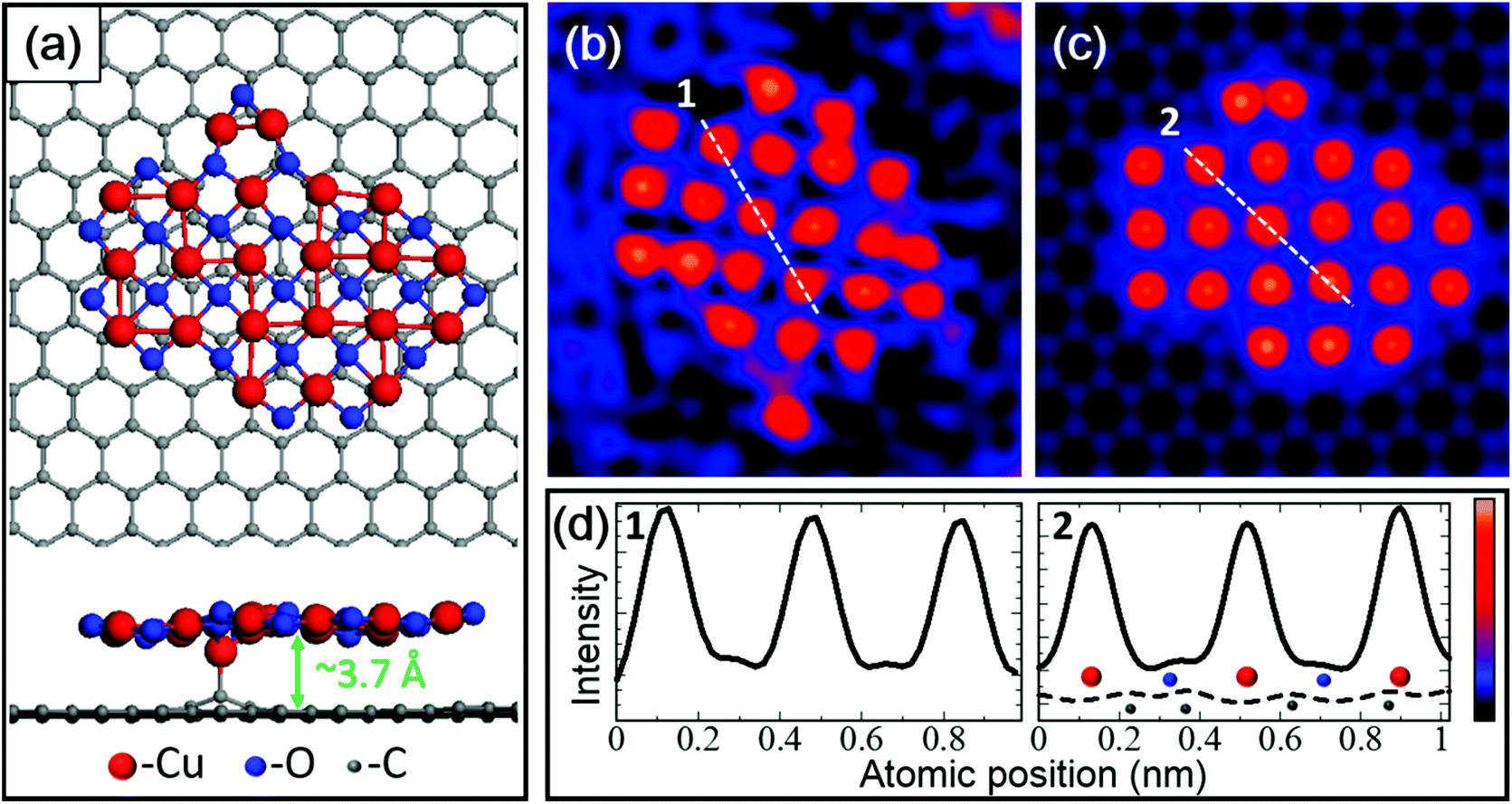 | ||
| Fig. 2 Comparison between the experimental and simulated data for the 2D copper oxide cluster. (a) Top and side views of the atomic model of the 2D copper oxide cluster after the DFT relaxation at 0 K. (b) Magnified and low-pass-filtered STEM images of the 2D cluster in Fig. 1b. (c) Simulated STEM image using the model of (a). (d) Line-profiles through the white lines marked in (b) and (c). In the simulated line profiles, the positions of Cu, O, and C atoms are illustrated by red, blue, and gray balls, respectively. The dashed line profile in (d) indicates the intensity of the separately simulated image of the graphene sheet without the 2D cluster. | ||
Our calculations show that the oxygen atoms tend to locate at the centre of the Cu squares; they strengthen the square lattice and suppress out-of-plane distortion. This configuration is unusual and might be intrinsic to 2D metal oxides. The position of oxygen atoms in 2D copper oxide was also confirmed by STEM. Fig. 2b and c are the experimental and simulated ADF-STEM images, and the intensity line profiles in Fig. 2d were obtained along the white dashed lines. The experimental line profile agrees well with the simulated one both for Cu and O atoms represented by the large and small peaks, respectively.
We calculated the activation energy and total energy change for the transformation between the 2D infinite sheets of copper oxide and pure copper (see ESI Fig. S2†), and found that oxygen atoms can easily fill in the square Cu lattice without an energy barrier, whereas desorption of oxygen requires huge energy penalty. These results explain how oxygen can stabilize 2D copper oxide, although we used simplified models not taking into account the effect of the underlying graphene substrate. DFT calculations further suggest that oxygen atoms at the cluster edges additionally stabilize the 2D square lattice. The edges of the 2D copper oxide cluster bind with graphene only when the graphene sheet has vacancy defects, and even in that case the other parts of the cluster can maintain its structure without strong bonding with graphene. This is in contrast to the edges of pure copper and copper carbide clusters, which are unstable and bind with the underlying graphene surface by distorting their structures.
Properties of 2D copper oxide
The unusual atomic geometry of 2D copper oxide leads to unexpected electronic and magnetic properties. 2D copper oxide is predicted to have semiconducting properties with a band gap of 2.7 eV, and major contributions of Cu states at the bottom of the conduction band and O states at the top of the valence band (see ESI Fig. S3†). In contrast, bulk CuO is a semiconductor with a band gap of ∼1.5 eV.19 Furthermore, 2D copper oxide has an antiferromagnetic ground state (see ESI Fig. S4†), whereas bulk Cu and CuO are paramagnetic.We also estimated the in-plane stiffness of 2D copper oxide to be 123.7 N m−1 by ab initio calculation, which is lower than that of graphene (340 N m−1),20 but comparable to those of TMD materials (123–180 N m−1 for single-layer MoS2 and WS2).21–23 2D copper oxide has a high stiffness because Cu and O atoms in the 2D sheet form strong covalent bonds with the binding energy of 4.07 eV. In addition, the mechanical stability of the 2D cluster against bending was examined by comparing the total energy of flat 2D copper oxide with copper oxide nanotubes and was studied at the DFT-PBE level (see ESI Fig. S5a and b†). Calculations by this approach show that the copper oxide nanotube with a finite radius (>0.5 nm) is energetically more stable than the 2D sheet, implying the necessity of graphene as a supporting material of the 2D copper oxide.
Molecular dynamics (MD) simulations further suggest that a small 2D copper oxide cluster (∼1.4 nm in lateral size) on graphene has a curved structure slightly displaced from the graphene surface by keeping its square lattice at 300 K (see ESI Fig. S5c†). The MD simulation at 600 K also shows that 2D copper oxide cluster on graphene started to melt in a short time (∼0.25 ns). These results explain the experimental fact that the 2D copper oxide clusters were observed in the present study at room temperature, but not observed when the sample was heated at 300 °C.
Conclusions
We have demonstrated and characterized one-atom-thick 2D copper oxide clusters with an unusual square lattice on graphene. STEM-EELS observations and DFT modelling reveal that oxygen is located at the centre of the square Cu lattice and thereby stabilizes it. Calculations show that 2D copper oxide has wide-gap semiconducting properties and antiferromagnetic spin ordering different from bulk copper oxide. We believe that the present results will pave the way for the investigation of novel 2D nanostructures with an unusual lattice geometry.Methods
Sample preparation
Single-layer graphene on Cu foil was transferred onto TEM grids using the previously reported poly(methyl methacrylate) support method.24,25 The grids were made of gold covered with an amorphous carbon film with 2 µm diameter holes (Quantifoil®, Quantifoil Micro Tools GmbH). To avoid metallic impurities we etched the Cu foil with a metal-free (NH4)2S2O8 solution. Cu was then deposited using an ion beam etching system (PECS, Gatan Inc.). The samples were exposed to the atmosphere before STEM experiments, which consequently leads to incorporations of oxygen and hydrocarbon species. These were attracted as contamination to the region where the focused electron beam was irradiated, therefore, further contamination was suppressed by wide-area electron-beam irradiation of the sample inside the microscope prior to high-resolution observations. The number of graphene layers was confirmed by dark-field TEM imaging26 prior to STEM, and we selected the single-layer region.STEM-EELS experimental conditions
An aberration-corrected microscope (JEM-ARM200F, JEOL Ltd) was operated at a low voltage of 80 kV to reduce knock-on damage to the sample. The angular range of electrons collected in the ADF detector was about 46–161 mrad. The incident beam current was ∼55 pA, and a typical dose was ∼105 electrons per Å2 per image. All the results about 2D copper oxide were obtained at room temperature, while the EEL spectrum of 3D pure Cu in Fig. 1f was obtained at 300 °C in TEM-mode (beam irradiated area was ∼20 nm in diameter). Such annealing reduced oxygen and led most of the Cu aggregates into 3D nanoparticles (∼5 nm in diameter). To improve the signal-to-noise ratio, STEM images shown in Fig. 1c, d, and 2b were low-pass filtered, and the green EEL spectrum of 2D copper oxide in Fig. 1f was spatially averaged.STEM image simulation
Image simulation was performed using multislice software (xHREM™, HREM Research Inc.) under the following conditions: the aperture radius (convergence semi-angle) 28.4 mrad, third- and fifth-order spherical aberration coefficients 5 µm, ADF detector angle 46–161 mrad, and probe size 0.8 Å. Simulations included thermal diffuse scattering absorption with the Debye–Waller factors of each element taken from the literature.27–29First-principles calculations
All calculations of the atomic structure and stability of the 2D copper oxide were performed using DFT within the Perdew–Burke–Ernzerhof (PBE) functional.30 We used the projector augmented wave method31 approximation with the periodic boundary conditions and a Vienna Ab initio Simulation Package.32–35 The plane-wave energy cut-off was set to 450 eV. To calculate the equilibrium atomic structures, the Brillouin zone was sampled according to the Monkhorst–Pack scheme36 with a 16 × 16 × 1 grid in the k space. The structural relaxation was performed until the forces acting on each atom became less than 0.001 eV Å−1. The model of the 2D copper oxide cluster on graphene consisted of 161 carbon atoms, 22 copper atoms and 24 oxygen atoms, including atoms at the cluster edges. The cell size was larger than 15 Å to avoid the interaction between the clusters. The evolution of the CuO cluster structure at the finite constant temperature was described in the framework of the MD simulations using the Nosé–Hoover thermostat.37,38 The temperature was set at 300 K and 600 K to match the experimental conditions. The total time of the simulations was 0.45 ns with a time step of 1 fs. The atomic structure was written after every ionic step. For investigation of the stability, elastic, electronic and magnetic properties, we used infinite models with the unit cell consisted of 4 copper atoms and 4 oxygen atoms. The electronic properties of the CuO layer were studied using the DFT+U approach suggested by Dudarev et al.39Note added in proof
After the work was submitted, the paper dealing with CuO monolayer observation appeared. Yin et al.40 independently investigated the specific atomic structure of the 2D CuO using STEM and DFT methods with results generally supporting our conclusions.Acknowledgements
We thank Dr P. V. Avramov, Dr K. Iakoubovskii, Dr L. Yu. Antipina, Dr Z. I. Popov and Dr H. Naramoto for fruitful discussions. A part of this work was supported by the ‘Nanotechnology Platform Project’ and ‘MEXT Program for Development of Environmental Technology using Nanotechnology’ sponsored by the Ministry of Education, Culture, Sports, Science and Technology (MEXT), Japan, and JSPS KAKENHI Grant Numbers 15J04118, 25390035 and 16H03875, Japan. D. G. K., S. S and P. B. S. gratefully acknowledge the financial support of the Ministry of Education and Science of the Russian Federation in the framework of Increase Competitiveness Program of NUST “MISiS” (no. K2-2015-033). D. G. K. and P. B. S. are grateful to the supercomputer cluster “Cherry” provided by the Materials Modelling and Development Laboratory at NUST “MISIS” (supported via the Grant from the Ministry of Education and Science of the Russian Federation no. 14.Y26.31.0005), to the cluster computer ‘Lomonosov’ provided by Moscow State University and to the Joint Supercomputer Center of the Russian Academy of Sciences. L. A. C. acknowledges the financial support of the Russian Science Foundation (project no. 14-12-01217). P. B. S. acknowledges the financial support of the RFBR, according to the research project no. 16-32-60138 mol_a_dk.References
- K. S. Novoselov, A. K. Geim, S. V. Morozov, D. Jiang, Y. Zhang, S. V. Dubonos, I. V. Grigorieva and A. A. Firsov, Science, 2004, 306, 666–669 CrossRef CAS PubMed.
- A. K. Geim and K. S. Novoselov, Nat. Mater., 2007, 6, 183–191 CrossRef CAS PubMed.
- N. Alem, R. Erni, C. Kisielowski, M. D. Rossell, W. Gannett and A. Zettl, Phys. Rev. B: Condens. Matter, 2009, 80, 155425 CrossRef.
- L. Song, L. Ci, H. Lu, P. B. Sorokin, C. Jin, J. Ni, A. G. Kvashnin, D. G. Kvashnin, J. Lou, B. I. Yakobson and P. M. Ajayan, Nano Lett., 2010, 10, 3209–3215 CrossRef CAS PubMed.
- Q. H. Wang, K. Kalantar-Zadeh, A. Kis, J. N. Coleman and M. S. Strano, Nat. Nanotechnol., 2012, 7, 699–712 CrossRef CAS PubMed.
- M. Osada and T. Sasaki, Adv. Mater., 2012, 24, 210–228 CrossRef CAS PubMed.
- R. Mas-Ballesté, C. Gómez-Navarro, J. Gómez-Herrero and F. Zamora, Nanoscale, 2011, 3, 20–30 RSC.
- C. L. Freeman, F. Claeyssens, N. L. Allan and J. H. Harding, Phys. Rev. Lett., 2006, 96, 66102 CrossRef PubMed.
- P. B. Sorokin, A. G. Kvashnin, Z. Zhu and D. Tománek, Nano Lett., 2014, 14, 7126–7130 CrossRef CAS PubMed.
- H. T. Quang, A. Bachmatiuk, A. Dianat, F. Ortmann, J. Zhao, J. H. Warner, J. Eckert, G. Cunniberti and M. H. Rümmeli, ACS Nano, 2015, 9, 11408–11413 CrossRef CAS PubMed.
- J. Zhao, Q. Deng, A. Bachmatiuk, G. Sandeep, A. Popov, J. Eckert and M. H. Rummeli, Science, 2014, 343, 1228–1232 CrossRef CAS PubMed.
- Y. Shao, R. Pang and X. Shi, J. Phys. Chem. C, 2015, 119, 22954–22960 CAS.
- C. Tusche, H. L. Meyerheim and J. Kirschner, Phys. Rev. Lett., 2007, 99, 26102 CrossRef CAS PubMed.
- J. Lee, D. C. Sorescu and X. Deng, J. Phys. Chem. Lett., 2016, 7, 1335–1340 CrossRef CAS PubMed.
- O. L. Krivanek, M. F. Chisholm, V. Nicolosi, T. J. Pennycook, G. J. Corbin, N. Dellby, M. F. Murfitt, C. S. Own, Z. S. Szilagyi, M. P. Oxley, S. T. Pantelides and S. J. Pennycook, Nature, 2010, 464, 571–574 CrossRef CAS PubMed.
- C. C. Ahn, Transmission Electron Energy Loss Spectrometry in Materials Science and the EELS Atlas, 2006 Search PubMed.
- R. D. Leapman, L. A. Grunes and P. L. Fejes, Phys. Rev. B: Condens. Matter, 1982, 26, 614–635 CrossRef CAS.
- S. L. Hulbert, B. A. Bunker, F. C. Brown and P. Pianetta, Phys. Rev. B: Condens. Matter, 1984, 30, 2120–2126 CrossRef CAS.
- M. Heinemann, B. Eifert and C. Heiliger, Phys. Rev. B: Condens. Matter, 2013, 87, 115111 CrossRef.
- C. Lee, X. Wei, J. W. Kysar and J. Hone, Science, 2008, 321, 385–388 CrossRef CAS PubMed.
- Z. Fan, Z. Wei-Bing and T. Bi-Yu, Chin. Phys. B, 2015, 24, 97103 CrossRef.
- J. Kang, S. Tongay, J. Zhou, J. Li and J. Wu, Appl. Phys. Lett., 2013, 102, 12111 CrossRef.
- D. Çakır, F. M. Peeters and C. Sevik, Appl. Phys. Lett., 2014, 104, 203110 CrossRef.
- E. Kano, M. Takeguchi, J. Fujita and A. Hashimoto, Carbon, 2014, 80, 382–386 CrossRef CAS.
- E. Kano, A. Hashimoto, T. Kaneko, N. Tajima, T. Ohno and M. Takeguchi, Nanoscale, 2016, 8, 529–535 RSC.
- P. Y. Huang, C. S. Ruiz-Vargas, A. M. van der Zande, W. S. Whitney, M. P. Levendorf, J. W. Kevek, S. Garg, J. S. Alden, C. J. Hustedt, Y. Zhu, J. Park, P. L. McEuen and D. A. Muller, Nature, 2011, 469, 389–392 CrossRef CAS PubMed.
- J. S. Reid, Acta Crystallogr., Sect. A: Found. Crystallogr., 1983, 39, 1–13 CrossRef.
- V. F. Sears and S. A. Shelley, Acta Crystallogr., Sect. A: Found. Crystallogr., 1991, 47, 441–446 CrossRef.
- H. X. Gao and L.-M. Peng, Acta Crystallogr., Sect. A: Found. Crystallogr., 1999, 55, 926–932 CrossRef.
- J. P. Perdew, K. Burke and M. Ernzerhof, Phys. Rev. Lett., 1996, 77, 3865–3868 CrossRef CAS PubMed.
- P. E. Blöchl, Phys. Rev. B: Condens. Matter, 1994, 50, 17953–17979 CrossRef.
- G. Kresse and J. Furthmüller, Comput. Mater. Sci., 1996, 6, 15–50 CrossRef CAS.
- G. Kresse and J. Furthmüller, Phys. Rev. B: Condens. Matter, 1996, 54, 11169–11186 CrossRef CAS.
- G. Kresse and J. Hafner, Phys. Rev. B: Condens. Matter, 1993, 47, 558–561 CrossRef CAS.
- G. Kresse and J. Hafner, Phys. Rev. B: Condens. Matter, 1994, 49, 14251–14269 CrossRef CAS.
- H. J. Monkhorst and J. D. Pack, Phys. Rev. B: Condens. Matter, 1976, 13, 5188–5192 CrossRef.
- W. G. Hoover, Phys. Rev. A, 1985, 31, 1695–1697 CrossRef.
- S. Nosé, J. Chem. Phys., 1984, 81, 511–519 CrossRef.
- S. L. Dudarev, G. A. Botton, S. Y. Savrasov, C. J. Humphreys and A. P. Sutton, Phys. Rev. B: Condens. Matter, 1998, 57, 1505–1509 CrossRef CAS.
- K. Yin, Y.-Y. Zhang, Y. Zhou, L. Sun, M. F. Chisholm, S. T. Pantelides and W. Zhou, 2D Mater., 2017, 4, 11001 CrossRef.
Footnote |
| † Electronic supplementary information (ESI) available: Additional calculated data of pure Cu and carbide, energy diagram of simplified transformation, and electronic, magnetic and bending properties. See DOI: 10.1039/c6nr06874j |
| This journal is © The Royal Society of Chemistry 2017 |