
 Open Access Article
 This Open Access Article is licensed under a
 Creative Commons Attribution 3.0 Unported Licence
Controlling electronic access to the spin excitations of a single molecule in a tunnel junction†
Ben
Warner
ab,
Fadi
El Hallak‡
a,
Henning
Prüser
a,
Afolabi
Ajibade
ab,
Tobias G.
Gill
ac,
Andrew J.
Fisher
ab,
Mats
Persson
 de and
Cyrus F.
Hirjibehedin
*abc
de and
Cyrus F.
Hirjibehedin
*abc
aLondon Centre for Nanotechnology, University College London (UCL), London WC1H 0AH, UK. E-mail: c.hirjibehedin@ucl.ac.uk
bDepartment of Physics & Astronomy, UCL, London WC1E 6BT, UK
cDepartment of Chemistry, UCL, London WC1H 0AJ, UK
dSurface Science Research Centre and Department of Chemistry, University of Liverpool, Liverpool, L69 3BX, UK
eDepartment of Applied Physics, Chalmers University of Technology, SE-412 96, Göteborg, Sweden
First published on 6th March 2017
Abstract
Spintronic phenomena underpin new device paradigms for data storage and sensing. Scaling these down to the single molecule level requires controlling the properties of current-carrying molecular orbitals to enable access to spin states through phenomena such as inelastic electron tunnelling. Here we show that the spintronic properties of a tunnel junction containing a single molecule can be controlled using the local environment as a pseudo-gate. For tunnelling through iron phthalocyanine (FePc) on an insulating copper nitride (Cu2N) monolayer above Cu(001), we find that spin transitions may be strongly excited depending on the binding site of the central Fe atom. Different interactions between the Fe and the underlying Cu or N atoms shift the Fe d orbitals with respect to the Fermi energy and control the relative strength of the spin excitations; this effect is captured in a simple co-tunnelling model. This work demonstrates the importance of the atomic-scale environment for the development of single molecule spintronic devices.
The ability to manipulate the energy levels of a quantum mechanical system facilitates control over its properties. For example, gating controls energy level alignment in systems such as quantum dots or single molecule junctions,1,2 enabling electronic transport to be tuned between different regimes, such as a Coulomb blockade and Kondo screening.2,3 At the atomic scale, it has recently been shown that such gating effects also can be manipulated through the precise positioning of charged dopants.4–6
In electronic transport through a single molecule, the energy of the molecular orbitals can also control how the transport properties couple to local electronic or magnetic excitations of the molecule. Spintronic coupling can be demonstrated, for example, through inelastic spin transitions excited by a tunnelling current.7–9 The coupling of the spin to the tunnel current also enables spin excitation spectroscopy, in which inelastic tunnelling processes appear as steps in the differential conductance dI/dV at voltages corresponding to the energy of the excitations.9 This allows for the identification of spin excitation energies as in other spectroscopic techniques such as electron spin resonance, but with single-atom resolution. Such experiments allow for the measurement of g-factors,7 magnetic anisotropy.10 spin coupling energies,11 and spin dynamics12,13 in atomically precise spin systems.
The local environment significantly affects the magnetic properties of a single atom.14–16 This can be controlled by placing magnetic atoms in a molecular framework. Spin excitations in such magnetic molecules have been observed in nanojunctions,17,18 including those formed using a scanning tunnelling microscope.19–21
The factors controlling the strength of the spin excitations (i.e. the fraction of tunnelling electrons that result in inelastic excitations) have only begun to be explored experimentally.22 This is a significant limitation in advancing the measurement of spin excitations in nanojunctions, and therefore atomic-scale spintronic applications. The strength of the spin excitations can vary dramatically, from a few percent to well over 50 percent,11 and changes from molecule to molecule even on the same surface; for example, on the thin insulator boron nitride, spin excitations are observed for Mn12![[thin space (1/6-em)]](https://www.rsc.org/images/entities/char_2009.gif) 23 but not for CoPc.24 Developing an understanding of when and how strongly spin excitations are manifested in the tunnel current is therefore crucial.
23 but not for CoPc.24 Developing an understanding of when and how strongly spin excitations are manifested in the tunnel current is therefore crucial.
Here we report how the local environment can be used to modify the spintronic properties of a tunnel junction containing a single iron phthalocyanine (FePc) molecule on an insulating copper nitride (Cu2N) monolayer above Cu(001). Using scanning tunnelling microscopy (STM), we observe that spin transitions are strongly excited based on the binding site of the central Fe atom. We use both density functional theory and a co-tunnelling model to show that the striking difference in the strength of the spin excitations results from the modification of energy of the Fe d orbitals with respect to the Fermi energy due to the different interaction strength between the Fe and the underlying Cu or N atom.25 This work demonstrates that atomic scale molecule–substrate coupling could play a vital role in the development of spintronic devices26,27 based on single molecules.
In this experiment (see ESI†), FePc molecules were sublimed onto a room temperature Cu(001) substrate on which a Cu2N monolayer had been prepared.28 A low temperature scanning tunnelling microscopy topograph of the surface is shown in Fig. 1a, and in it the FePc molecules can be seen at the center of a large Cu2N island. The molecules are observed to bind in various locations on the surface, including next to step edges and defects, but here we focus on molecules near the centre of the islands. The FePc is observed to bind at all rotational angles, with preferences for 0°, 18°, 45° from the major crystal axis (Fig. S1†). DFT calculations of FePc molecules on the Cu2N monolayer show that there is little difference in the binding energy between different binding angles (<0.15 eV).28
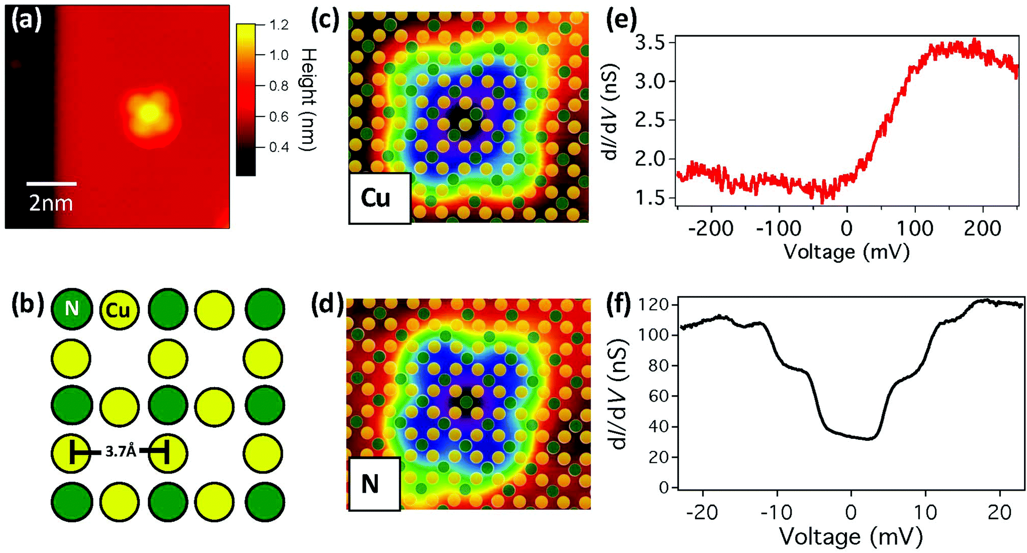 | ||
| Fig. 1 Single FePc molecule junction. (a) STM topograph of FePc on a Cu2N monolayer on Cu(001) (Vset = −1 V, Iset = 0.1 nA). (b) Illustration of the Cu2N surface, with Cu (yellow) and N (green) atoms. (c) STM topograph of FePc-Cu molecule on Cu2N. Yellow and greed dots indicate the positions of the underlying Cu and N atoms respectively, as determined from atomic resolution images of the surrounding Cu2N area (4.5 nm × 3.7 nm; Vset = 0.5 V, Iset = 0.5 nA). (d) Same as (c) for FePc-N on Cu2N. (e) dI/dV measurements above the central Fe atom in FePc-Cu, showing an onset in LDOS (Vset = −0.25 V, Iset = 0.5 nA). (f) dI/dV measurements above the central Fe atom in FePc-N, showing IET steps (Vset = −22 mV, Iset = 1.5 nA, B = 0.5 T). | ||
In the Cu2N surface, the N atoms form a c(2 × 2) reconstruction in the hollow sites of the Cu(001) surface, as shown in Fig. 1b. Previous work on Cu2N has shown that it is possible to resolve the atomic lattice of the surface with STM, and that the appearance varies with the applied bias voltage Vb.29 Using atomically resolved images of FePc on Cu2N, we observe that molecules bind exclusively with the central Fe atom either on top of Cu (FePc-Cu) or N (FePc-N) sites, as shown in Fig. 1c and d respectively. No substantial difference is apparent in the distribution of binding angles between FePc-Cu and FePc-N (Fig. S1†).
However, in differential conductance dI/dV measurements at low bias, a striking difference is observed between molecules on the two binding sites, as shown in Fig. 1c and d. For FePc-Cu, a feature in dI/dV is observed at a voltage of approximately 150 mV, with a width of approximately the same voltage. In sharp contrast, for FePc-N steps in dI/dV appear symmetrically at positive and negative bias at voltages in the ±20 mV regime. As seen in Fig. S2,† the dI/dV spectrum for FePc-Cu does not vary significantly from molecule to molecule. On the other hand, the steps observed in dI/dV for FePc-N molecules do vary in number (with two to three steps being clearly visible) and in energy but are always present (Fig. S2†). No systematic dependence on either of these changes has been correlated with binding angle or distance from the boundaries of the Cu2N islands, suggesting that they may arise from small changes in the local environment of the FePc (e.g. as seen in ref. 14).
The broad feature observed in the low bias spectroscopy of FePc-Cu can be associated with features in the local density of states (LDOS). On the other hand, symmetric steps in dI/dV are naturally associated with inelastic electron tunnelling (IET),9 which can arise from vibrational,30 rotational,31,32 or spin and orbital7,10,11,13,16 excitations. The shift of the FePc-N excitations with magnetic field (Fig. S3†) suggests that they arise from magnetic excitations (see ESI†). Similar IET due to spin excitations has also been observed when FePc is deposited on copper oxide surfaces.20
An isolated FePc molecule has been shown to have S = 1,33 and prior measurements of FePc on CuO indicate that the molecule retains its spin on the surface.20 DFT calculations for FePc on Cu2N have shown that the spin of the Fe atom is S = 1 for both FePc-Cu and FePc-N.28 This suggests that changes in net spin of the molecule cannot explain the difference observed in the spectroscopic measurements on the different Cu2N binding sites (i.e. that IET steps are not absent in FePc-Cu because the total spin has changed).
Although simple transition matrix elements can be utilized to calculate the relative intensities of inelastic spin transitions,10 calculations have shown that the overall magnitude relative to elastic tunnelling depends on the energy of the orbitals involved in the multistep IET processes with respect to the Fermi energy EF.25 Therefore, we carried out detailed DFT calculations (see ESI†) to investigate the effect of binding site on the orbital energies. In DFT calculations for a given binding site, we observe minimal change with rotation angle in the energy of the orbitals and the magnetic moment. Therefore, here we only consider the effect of changing the binding site on the properties of the molecule.
As shown in Fig. 2d, the partial density of states (PDOS) of the orbitals with d-character for the isolated FePc show strong exchange splitting with a large gap between occupied and unoccupied levels. Interestingly, similar results are also observed for FePc-Cu (Fig. 2e). The interaction with the surface results in a slight broadening of the levels and a shift in the position of the orbitals with respect to EF. Furthermore, the Fe atom is 3.2 Å above the Cu atom in the surface, suggesting that FePc-Cu is physisorbed and only weakly interacting with the surface.
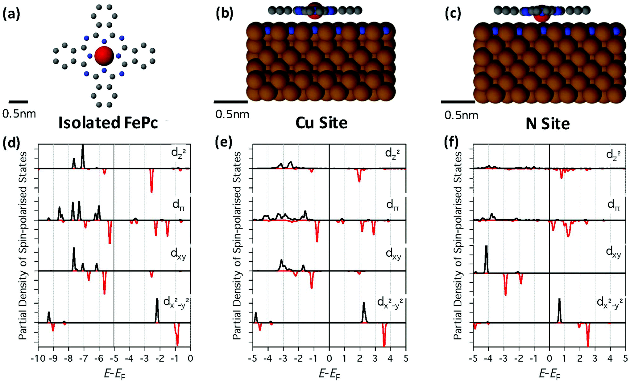 | ||
| Fig. 2 Calculated structure and orbital DOS for FePc on Cu2N. (a) Atomic structure of isolated FePc as calculated using DFT; C, N, and Fe atoms are shown in grey, blue, and red respectively, while H atoms are not shown for clarity. (b) Atomic structure of FePc-Cu at 0° from the [100] axis as calculated by DFT; Cu atoms are shown in brown. (c) Same as (b) for FePc-N. (d) PDOS for spin-polarized states as projected onto the Fe d-orbitals (as labeled) of an isolated FePc for majority (black) and minority (red) spin states. A large gap in the PDOS is seen around EF. (e) Same as (d) for FePc-Cu. The states are essentially aligned to the vacuum level and some are also slightly broadened. This suggests that the molecule is only weakly interacting with the surface. Note that the maximum energy corresponds to the vacuum level. (f) Same as (e) for FePc-N. In this case, the orbitals are shifted closer to EF, and this is due to the stronger interaction of FePc-N with the surface than FePc-Cu. Note that the PDOS are Gaussian-broadened by 0.1 eV. | ||
In dramatic contrast, for FePc-N the Fe atom is pulled down to 2.03 Å above the N and the N atom in the surface is also shifted upwards by 0.76 Å, suggesting the FePc-N is chemisorbed and interacting with the surface more strongly than FePc-Cu. As seen in Fig. 2f, this strong interaction results in an overall downward shift in the molecular orbitals with respect to EF as well as a noticeable broadening.
This difference in bonding character between the two sites results in the Fe d-orbitals being much closer to EF for FePc-N than for FePc-Cu, as shown in Fig. 3, where the calculated LDOS at 0.62 nm above the Fe atom are compared to dI/dV measurements obtained above the respective molecules. We observe that the calculated LDOS is dominated by the contribution from states with dz2 character. Fig. 3a shows that for FePc-Cu there is almost no LDOS around EF. In sharp contrast, however, for FePc-N (Fig. 3b) strong features are clearly seen close to EF both in the DFT calculations and in the measured dI/dV spectra.
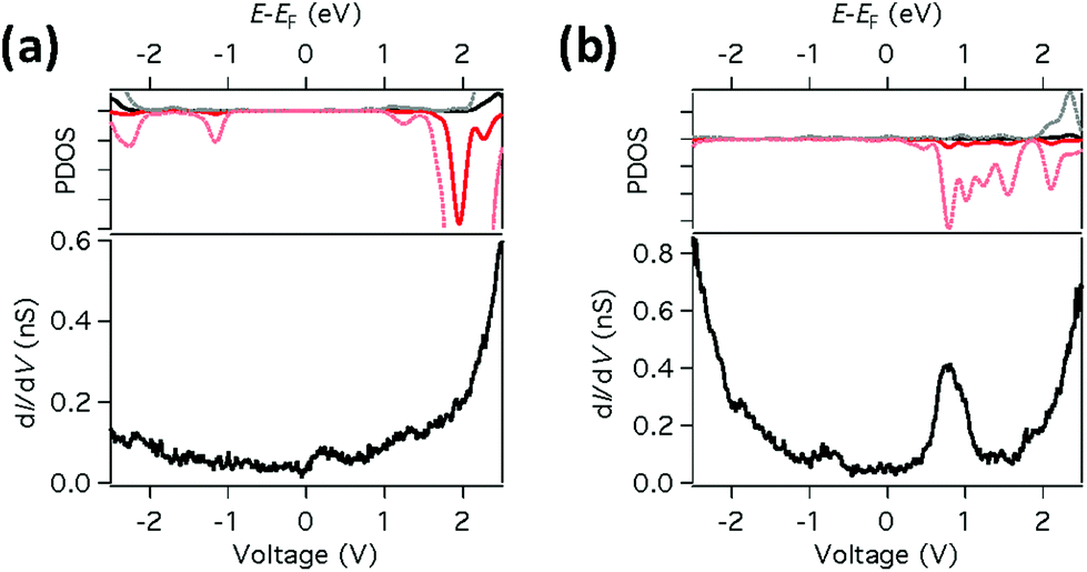 | ||
| Fig. 3 Comparison of calculated LDOS with dI/dV spectroscopy. (a) Calculated LDOS and high voltage dI/dV spectroscopy taken on top of the Fe atom in FePc-Cu (Vset = 2.5 V, Iset = 0.5 nA). No distinct features are seen between ±2 V in the PDOS or dI/dV. The dashed lines correspond a magnification of 10 times. The LDOS was calculated at a tip-Cu surface distance of 0.62 nm on top of the Fe atom. (b) Same as (a) for FePc-N. Here, distinct spin-polarized states appear in the LDOS near +1.0 V; corresponding features are also seen in dI/dV. | ||
For both binding sites (i.e. FePc-Cu and FePc-N) there is some variation in the measured high voltage spectra (see Fig. S4†). This variation may be due to the atomic-scale environment on which each molecule sits (e.g. nearby step edges and defects). However, the main features of the two sites are consistent and we do not observe any systematic changes due to binding angle. This suggests that the ligands are not playing a significant role in determining the characteristics of the tunnelling through the Fe atom.
To understand the relationship of the spin-dependent tunnelling to the electronic structure, we analysed a simple co-tunnelling model25 (see ESI†). In addition to the direct tunnelling between tip and surface, we considered electrons tunnelling via a molecular system containing a localized spin with S = 1; this co-tunnelling process occurs via an (n + 1)-electron (excited) intermediate molecular state; hole transport via the (n − 1)-electron state is neglected for simplicity. While in the virtual intermediate state, the tunnelling electron interacts with the localized spin via an exchange interaction, characterized by an exchange constant J. As a result, the tunnelling process can change the spin state of the molecular system, giving rise to spin-dependent transport. We note that this model is only valid in the limit of virtual transitions, and therefore is not quantitatively valid when the affinity levels are close to the Fermi energy EF (i.e. when the strongest enhancement of the inelastic transition rate is expected). However, the general trends observed in this model when these levels are far from the Fermi energy should continue when they approach the Fermi energy.
As seen in Fig. 4, as the excitation energy for the charging process increases (corresponding to the virtual orbitals moving further from EF) all co-tunnelling processes (labeled CT1 and CT2) are suppressed while the direct tunnelling (DT) processes remain unaffected. However, we find that the terms describing spin-dependent co-tunnelling transport (CT2), including inelastic transport, decay more quickly than those that describe spin-independent co-tunnelling transport (CT1); these different decays correspond to the appearance of different powers of the molecular charging energy in the relevant energy denominators (see ESI†). We note that co-tunnelling terms that involve other orbitals (e.g. s and p orbitals) would not be affected by the changes in energy of the d orbitals, and therefore would produce a constant elastic tunnelling contribution similar to DT.
 | ||
| Fig. 4 Co-tunnelling model. (a) Schematic of the co-tunnelling model, in which three processes can occur: spin independent co-tunnelling (CT1), spin dependent co-tunnelling (CT2), and direct tunnelling (DT). The charging energy U represents the central energy of the set of molecular levels Ei, eV is the shift in energy from the applied bias voltage Vb with e being the electronic charge, and Ef is the Fermi energy. (b) Representation of the tunnelling as the molecule level moves away from the Fermi energy. A sharper drop occurs with U − Ef in CT2 than CT1, with no change in DT. | ||
Hence, for FePc-Cu, where the affinity levels are far from EF (Fig. 3a), the spin-dependent transport is strongly suppressed, both relative to direct tunnelling and relative to spin-independent co-tunnelling contributions. However, for the case of FePc-N, where the orbitals are closer to EF owing to the molecule's stronger interaction with the surface (Fig. 3b), we expect not only stronger tunnelling overall but also a significantly larger spin-dependent inelastic fraction, favouring the observation of spin excitations in IET spectroscopy.
As seen in Fig. 1c, for FePc-Cu we do observe a small feature in the dI/dV spectra at low bias. Since no d-DOS is observed near the Fermi energy in our DFT calculations, we assign this feature to a many-body bonding state between the d states and the ligand states.34 It is interesting to note that the IET transition intensities are low for FePc-Cu even though this resonance is close to the Fermi energy. This suggests that this state does not play a significant role in the IET spin excitation process.
This experiment demonstrates that surface interactions can be used to manipulate the strength of the exchange coupling between tunnelling electrons and a molecular spin in a single molecule junction by changing the relative energy of the relevant orbitals. Since the energy levels of the molecule can be controlled by choosing the appropriate materials that compose the junction, these surface interactions can be used as an effective gate at the atomic scale. Furthermore, it may be possible to modify the energy level alignment in a controlled manner and also to select a preferred binding site for the molecule on the surface through the additional functionalization of the molecule. This highlights the fact that atomic-scale control of a tunnel junction is useful when developing viable single molecule spintronic devices, just as surface and interface bonding can control spin-dependent tunnelling in planar magnetic35 and multiferroic tunnel junctions.36
Acknowledgements
We acknowledge Joaquín Fernández Rossier, Sebastian Loth, Matteo Mannini, and Shichao Yan for stimulating discussions. B. W., F. E. H., H. P., A. A., A. J. F., and C. F. H. acknowledge financial support from the EPSRC [EP/H002367/1, EP/D063604/1, and EP/G036675/1] and the Leverhulme Trust [RPG-2012-754]. M. P. is grateful for allocations of computer resources at HECToR through the Materials Chemistry Consortium funded by EPSRC [EP/L000202/1] and at PDC through SNIC.References
- A. Riss, et al. , ACS Nano, 2014, 8, 5395 CrossRef CAS PubMed.
- M. L. Perrin, E. Burzuri and H. S. van der Zant, Chem. Soc. Rev., 2015, 44, 902 RSC.
- G. D. Scott and D. Natelson, ACS Nano, 2010, 4, 3560 CrossRef CAS PubMed.
- D. H. Lee and J. A. Gupta, Science, 2010, 330, 1807 CrossRef CAS PubMed.
- C. Uhlmann, I. Swart and J. Repp, Nano Lett., 2013, 13, 777 CrossRef CAS PubMed.
- J. Martínez-Blanco, et al. , Nat. Phys., 2015, 11, 640 CrossRef.
- A. J. Heinrich, J. A. Gupta, C. P. Lutz and D. M. Eigler, Science, 2004, 306, 466 CrossRef CAS PubMed.
- F. Delgado and J. Fernández-Rossier, Phys. Rev. B: Condens. Matter, 2010, 82, 134414 CrossRef.
- M. Ternes, New J. Phys., 2015, 17, 063016 CrossRef.
- C. F. Hirjibehedin, et al. , Science, 2007, 317, 1199 CrossRef CAS PubMed.
- C. F. Hirjibehedin, C. P. Lutz and A. J. Heinrich, Science, 2006, 312, 1021 CrossRef CAS PubMed.
- S. Loth, M. Etzkorn, C. P. Lutz, D. M. Eigler and A. J. Heinrich, Science, 2010, 329, 1628 CrossRef CAS PubMed.
- A. A. Khajetoorians, et al. , Phys. Rev. Lett., 2011, 106, 037205 CrossRef CAS PubMed.
- B. Bryant, A. Spinelli, J. J. T. Wagenaar, M. Gerrits and A. F. Otte, Phys. Rev. Lett., 2013, 111, 127203 CrossRef CAS PubMed.
- J. C. Oberg, et al. , Nat. Nanotechnol., 2014, 9, 64 CrossRef CAS PubMed.
- I. G. Rau, et al. , Science, 2014, 344, 988 CrossRef CAS PubMed.
- M.-H. Jo, et al. , Nano Lett., 2006, 6, 2014 CrossRef CAS PubMed.
- E. A. Osorio, et al. , Nano Lett., 2010, 10, 105 CrossRef CAS PubMed.
- X. Chen, et al. , Phys. Rev. Lett., 2008, 101, 197208 CrossRef PubMed.
- N. Tsukahara, et al. , Phys. Rev. Lett., 2009, 102, 167203 CrossRef PubMed.
- B. W. Heinrich, L. Braun, J. I. Pascual and K. J. Franke, Nat. Phys., 2013, 9, 765 CrossRef CAS.
- B. Bryant, et al. , Nano Lett., 2015, 15, 6542 CrossRef CAS PubMed.
- S. Kahle, et al. , Nano Lett., 2012, 12, 518 CrossRef CAS PubMed.
- F. Schulz, R. Drost, S. K. Hämäläinen and P. Liljeroth, ACS Nano, 2013, 7, 11121 CrossRef CAS PubMed.
- F. Delgado and J. Fernández-Rossier, Phys. Rev. B: Condens. Matter, 2011, 84, 045439 CrossRef.
- C. Chappert, A. Fert and F. N. Van Dau, Nat. Mater., 2007, 6, 813 CrossRef CAS PubMed.
- A. D. Kent and D. C. Worledge, Nat. Nanotechnol., 2015, 10, 187 CrossRef CAS PubMed.
- B. Warner, et al. , Nat. Nanotechnol., 2015, 10, 259 CrossRef CAS PubMed.
- T. Choi, C. Ruggiero and J. Gupta, Phys. Rev. B: Condens. Matter, 2008, 78, 035430 CrossRef.
- B. C. Stipe, M. A. Rezaei and W. Ho, Science, 1998, 280, 1732 CrossRef CAS PubMed.
- S. Li, et al. , Phys. Rev. Lett., 2013, 111, 146102 CrossRef PubMed.
- F. D. Natterer, F. Patthey and H. Brune, Phys. Rev. Lett., 2013, 111, 175303 CrossRef PubMed.
- J. Bartolomé, et al. , Phys. Rev. B: Condens. Matter, 2010, 81, 195405 CrossRef.
- J. Kügel, et al. , Nano Lett., 2014, 14, 3895 CrossRef PubMed.
- E. Y. Tsymbal, et al. , Prog. Mater. Sci., 2007, 52, 401 CrossRef CAS.
- J. P. Velev, S. S. Jaswal and E. Y. Tsymbal, Phil. Trans. R. Soc., A, 2011, 369, 3069 CrossRef CAS PubMed.
Footnotes |
| † Electronic supplementary information (ESI) available: Experimental, calculational, and computational details, including discussion of variations in tunnelling spectroscopy. See DOI: 10.1039/c6nr06469h. Additional experimental data can be found online. See DOI: 10.6084/m9.figshare.c.3699211 |
| ‡ Present address: Seagate Technology, Derry BT48 0BF, UK. |
| This journal is © The Royal Society of Chemistry 2017 |