
 Open Access Article
 This Open Access Article is licensed under a
 Creative Commons Attribution 3.0 Unported Licence
Self-directing chiral information in solid–solid transformation: unusual chiral-transfer without racemization from amorphous silica to crystalline silicon†
Xin-Ling
Liu
,
Seiji
Tsunega
and
Ren-Hua
Jin
 *
*
Department of Material and Life Chemistry, Kanagawa University, 3-27-1 Rokkakubashi, Kanagawa-ku, Yokohama 221-8686, Japan. E-mail: rhjin@kanagawa-u.ac.jp
First published on 26th January 2017
Abstract
Constructing novel chiral inorganic nanomaterials is an emerging branch in chirality research. In this work, by employing a solid magnesiothermic reaction at 500–600 °C, we reduced chiral SiO2 nanofibers with average diameter ∼10 nm into chiral Si nanoplates with a size of about several hundred nm. The chirality of the as-prepared Si was judged by the pair of signals with a mirror relationship between 400–500 nm that appeared on the solid-state diffuse reflectance circular dichroism (DRCD) spectra for the L- and D-form Si. Furthermore, the chirality was also confirmed by induced vibrational circular dichroism (VCD) signals corresponding to the absorption bands in the infrared range of achiral organics (polyvinylpyrrolidone K90 and trimethoxyphenylsilane) absorbed onto chiral Si. The as-used SiO2 nanofibers possessed an ultra high-temperature (up to 900 °C) resistant chirality, which would be due to the asymmetric arrangement of Si and O atoms in small chiral domains (<10 nm) on the Si–O–Si network of SiO2. During the removal of oxygen atoms from Si–O–Si by Mg atoms, the arrangement of newly formed Si–Si bonds as well as the growth of Si crystals were still templated without racemization from the chiral information in SiO2. Consequently, the subnano/nano-scale (<10 nm) chiral information was in situ transferred via the so-called self-transfer mechanism, even though there was no retention of the outward shapes of the length-scale nanofiber SiO2 reactants in the Si products. This work offers a feasible chemical method to prepare chiral Si using abundant SiO2 raw materials.
Conceptual insightsInorganic materials with chirality have been receiving increasing attention in the chirality research area. Most reported chiral inorganic materials are prepared by using helix-shaped organic (or inorganic) templates with helical pitch sizes over tens of nm. Such a chiral transfer is accomplished by copying the helical shapes, therefore, the destruction of them may lead to the disappearance of chirality. Herein, we propose a new concept of self-transfer of chiral information without racemization in solid–solid transformation similar to the molecular-scale, as demonstrated by the chemical reduction of chiral SiO2 nanofibers into chiral Si nanoplates at 500–600 °C. It was inferred that there are chiral domains (<7 nm) existing on the Si–O–Si network of the as-used SiO2, where the atomic arrangement of Si/O atoms is asymmetric and also high-temperature (up to 900 °C) resistant. Consequently, the formation of Si–Si bonds and the growth of the crystalline phase were regulated in situ by the chiral information of Si–O bonds, thus making Si chiral with the formation of defects. It is apparent in this process that neither additional chiral templates nor an outward chiral (helical) shape are necessary. This concept will open new avenues to understanding the origin of chirality and to promote the chiral design on inorganic nanomaterials. |
Introduction
Chirality is well known in organic chemistry as most biomolecules (L-amino acids, D-sugars, cholesterol, etc.) which are essential for our bodies, drugs, natural photosynthesis and optical display are chiral.1 On the other hand, chirality can also be found in some inorganic crystals and minerals (e.g., quartz and zeolite).2 In this regard, chirality is considered to be a fundamental property of the universe. However, research on the mutual chirality transfer between organic and inorganic systems is still limited. In addition, compared with chiral organic systems, less attention has been paid to chiral inorganic systems which should bring about new perspectives for the origin and universality of chirality and also chirality-related technologies.3 For chirality in inorganic crystals, chiral crystal structures can occur in the 65 types of the Sohncke crystallographic space groups. Even in metal crystals (e.g., Cu and Ag) with high symmetry, there are chiral crystal faces such as the fcc (643) and fcc (![[6 with combining macron]](https://www.rsc.org/images/entities/char_0036_0304.gif)
![[4 with combining macron]](https://www.rsc.org/images/entities/char_0034_0304.gif)
![[3 with combining macron]](https://www.rsc.org/images/entities/char_0033_0304.gif) ).4 Besides the intrinsic chirality of chiral crystal structures and/or the surfaces above, chirality can be acquired by designing various chiral appearances through site-selective chemical etching or high-temperature deposition, which usually need precise control, time-consuming steps or expensive equipment.5 Alternatively, chiral inorganic nanomaterials can easily be achieved by using chiral organics in three different fashions: (1) as chiral additives (Scheme 1a) to regulate the nucleation and growth of inorganic crystals, thus leading to the formation of intrinsically chiral phases, the preferable growth of chiral crystal faces and morphologies, or the production of chiral defects (e.g., screw dislocation);6 (2) as chiral binders (Scheme 1b) to modify the surface of inorganic nanoparticles (e.g., Au, Ag and CdSe) or connect these nanoparticles into special chiral configurations such as an asymmetric tetrahedron or helix;7 (3) as chiral shape templates (Scheme 1c), among which a series of helical organic assemblies have been used to prepare helical outward-forms of metal oxides (e.g., SiO2, TiO2, ZrO2) with observable pitches (within over tens of nanometers and micrometers).8 In these three cases, the chirality in the first is mainly from the intrinsic chirality present in these inorganic products, however, for the latter two, the chirality is greatly dependent on the existence of chiral organics, which is caused by the absorbed chiral molecules, the organic–inorganic interaction on the interfaces, or the chiral configurations/outward shapes maintained by these organics. Therefore, it may be roughly considered that the chirality transfer in these methods proceeds on the organic–inorganic heterogeneous interfaces (as shown in Scheme 2a), where the achiral inorganic clusters are arranged around the chiral organic surface to form geometrically asymmetric structures. When the organics are removed such as by heating, the deterioration of these chiral surfaces/interfaces, configurations and shapes may occur and then result in the disappearance of chirality. Hence, it is still a big challenge to maintain the chirality in the final inorganic systems.
).4 Besides the intrinsic chirality of chiral crystal structures and/or the surfaces above, chirality can be acquired by designing various chiral appearances through site-selective chemical etching or high-temperature deposition, which usually need precise control, time-consuming steps or expensive equipment.5 Alternatively, chiral inorganic nanomaterials can easily be achieved by using chiral organics in three different fashions: (1) as chiral additives (Scheme 1a) to regulate the nucleation and growth of inorganic crystals, thus leading to the formation of intrinsically chiral phases, the preferable growth of chiral crystal faces and morphologies, or the production of chiral defects (e.g., screw dislocation);6 (2) as chiral binders (Scheme 1b) to modify the surface of inorganic nanoparticles (e.g., Au, Ag and CdSe) or connect these nanoparticles into special chiral configurations such as an asymmetric tetrahedron or helix;7 (3) as chiral shape templates (Scheme 1c), among which a series of helical organic assemblies have been used to prepare helical outward-forms of metal oxides (e.g., SiO2, TiO2, ZrO2) with observable pitches (within over tens of nanometers and micrometers).8 In these three cases, the chirality in the first is mainly from the intrinsic chirality present in these inorganic products, however, for the latter two, the chirality is greatly dependent on the existence of chiral organics, which is caused by the absorbed chiral molecules, the organic–inorganic interaction on the interfaces, or the chiral configurations/outward shapes maintained by these organics. Therefore, it may be roughly considered that the chirality transfer in these methods proceeds on the organic–inorganic heterogeneous interfaces (as shown in Scheme 2a), where the achiral inorganic clusters are arranged around the chiral organic surface to form geometrically asymmetric structures. When the organics are removed such as by heating, the deterioration of these chiral surfaces/interfaces, configurations and shapes may occur and then result in the disappearance of chirality. Hence, it is still a big challenge to maintain the chirality in the final inorganic systems.
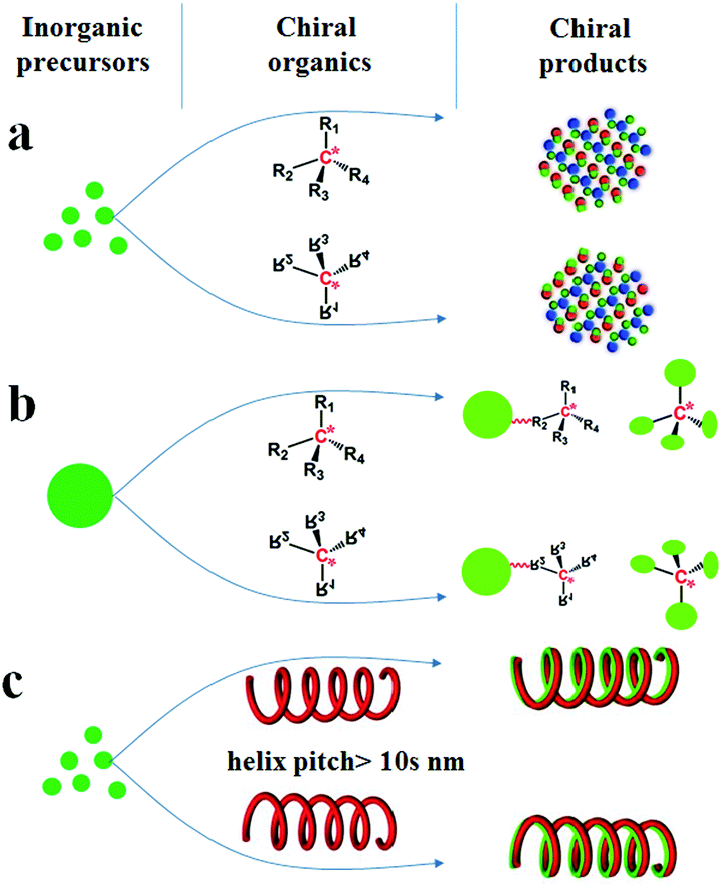 | ||
| Scheme 1 Three methods to prepare chiral inorganic nanomaterials by using chiral organic substances in three different fashions: (a) as chiral additives; (b) as chiral binders; (c) as chiral shape templates. | ||
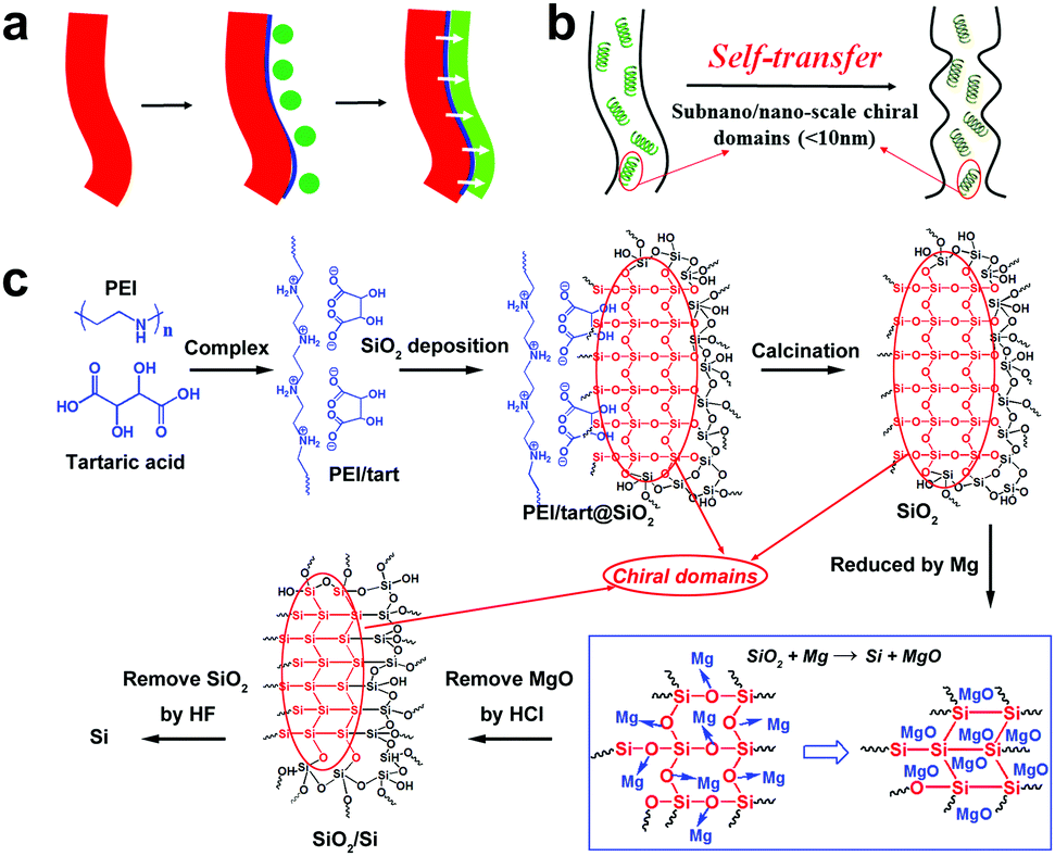 | ||
| Scheme 2 The schematic representation of (a) chirality transfer through heterogeneous interfaces (red parts represent the chirality sources, blue lines represent heterogeneous interfaces, green balls represent the precursors of newly-formed chiral products (green line), the white arrows show the chirality transfer); (b) the self-transfer of chiral information; (c) the formation process of chiral Si using PEI-(chiral tartaric acids) complexes (PEI/tart) as catalytic templates and chirality sources, and the areas marked with red ellipses correspond to the chiral domains shown in b. | ||
Compared to chiral transfer from organics to inorganics, the chirality transfer from the as-obtained chiral inorganics is also limited. Typically, they are used as (1) hard-templates to transfer the chiral shapes9 and (2) chiral hosts to produce inductive chirality on achiral guests.10 Usually, in of the both cases above, no chemical reactions occur on the chiral inorganic sources unless in order to remove them from the final products. The chirality transfer is also considered to be achieved on the heterogeneous interfaces (Scheme 2a). However, if these chiral inorganics were used as reactants, the chemical reactions occurring on themselves would lead to the destruction of chiral shapes and structures. In this way, it is difficult to maintain the chirality transfer in the solid–solid transformation from reactants to products. For example, despite the success in the template-assisted preparation of various helix-shaped chiral SiO2, there are seldom reports on their transformation into chiral Si. Recently, MacLachlan et al. showed a magnesiothermic reduction (Mg + SiO2 → Si + MgO) of a chiral nematic mesoporous SiO2 film into a mesoporous Si film.11 Unfortunately, no further optical characterizations such as circular dichroism (CD) spectra were conducted on the Si film to judge the chirality of Si. Nonetheless, after reduction, the initial chiral nematic order of SiO2 is destroyed, which means the failure of shape-chirality preservation in the final Si is possible. This is because this kind of chirality is based on the helical pitch at a larger length-scale (>tens of nm) but not on the asymmetric arrangement of atoms on a smaller molecular-like cluster length-scale. Therefore, the development of novel chirality transfer pathways is necessary. These pathways are especially desirable in the case of chiral inorganics themselves working as reactants to produce new chiral products via chemical reactions. Herein, we propose a new chirality transfer concept, namely the self-transfer (or chiral template-free) of chiral information in a solid–solid phase transformation without racemization on the molecular-like scale, which is shown in Scheme 2b. In this concept, there are many subnano/nano-scale (<10 nm) chiral domains distributed on chiral sources. In these domains, the arrangement of atoms can show some asymmetric features (e.g., molecular-like scaled helix). During the reaction, the chiral information (i.e., the asymmetric atomic arrangement) in these domains is also transferred in situ to the final products even if the outward shape of reactants is destroyed, which therefore regulates the breakage and formation of the chemical bonds in the chiral domains. In this case, additional chirality sources (shown in Scheme 2a) such as soft helical organic templates or hard helical inorganic templates are not necessary.
In this work, we used the chemical transformation of chiral SiO2 nanofibers into chiral Si to clarify this new chirality transfer mode. Although Si is an abundant element on earth, its crystalline form with a cubic structure shows high symmetry, which makes it difficult to construct chiral Si. Indeed, there are only several limited reports on chiral Si: (1) the absorption of chiral organic molecules on the surface of Si, yet the chirality is still from chiral organic molecules; (2) the growth of Si nanowires with transverse asymmetry on a Ag(110) surface by the deposition of Si atoms under vacuum and high temperature; (3) the selective-etching of Si wafers into various asymmetric-shaped Si products with shape-chirality on the length-scale of over tens of nm; (4) theoretical calculations on chiral Si wires, which demonstrate remarkable changes in atomic structures, electronic properties and energetic stability.12 Those chiral Si products produced above were obtained by using Si wafers or Si atoms as raw materials. However, to the best of our knowledge, there is no report on the self-transfer of chiral information (on the molecular-like scale) from silica (solid) to silicon (solid) via the direct chemical reduction of Si–O–Si bonds.
As pointed out above, it does not seem easy to obtain chiral Si using previously prepared helix-shaped chiral SiO2. Therefore, to fulfil the chirality transfer from SiO2 to Si, the chiral SiO2 sources are especially important. Recently, we established a convenient way to prepare chiral SiO2 by using crystalline chiral complexes as catalytic templates (Scheme 2c).13 The complexes consisted of polyethyleneimine (PEI) and chiral acids (e.g., tartaric acid and glucaric acid), and were self-assembled into one-dimensional structures in solution. Nanofiber-based chiral SiO2 was then produced by simply mixing the crystalline chiral complexes with the SiO2 source of tetramethoxysilane in an aqueous medium at room temperature for 1–2 h. The chirality of the silica remained after removing the organic components even by calcination at the high temperature of 900 °C. Different to the observable helix-shape chirality on chiral SiO2 reported by many groups, our chiral SiO2 has no outward helical shapes with ordered pitches. The former is produced via the conventional sol–gel process in which non-templated silica sols formed in the continuous phase deposited on helical templates to give outward helical shapes, while in the latter case, we propose that the silicification occurs directly around the chiral catalytic templates to give a chiral silica frame (i.e. chiral silica domain). Although the detailed reasons for the chirality on our SiO2 is not clear yet, it is considered that the subnano/nano-scale (ca. 5 nm) chiral domains (see the red domains marked with red ellipses in Scheme 2c) are randomly and densely distributed throughout the SiO2 network where the Si and O atoms arrange into an asymmetric cluster which displays a large chiroptical effect and high thermal-stability.13a Therefore, we expect that such chiral SiO2 would be an ideal candidate as the chiral source to prepare chiral Si via a direct chemical reduction process. Previously, we have succeeded in reducing SiO2 nanowires (obtained only by PEI template) into nano-structured Si via a low-temperature solid-state magnesiothermic reaction.14 Here, this method was further extended to reduce chiral SiO2, and the as-obtained reduced SiO2 was finally transformed into chiral Si by etching residual SiO2 with HF solution. Indeed, the solid-state diffuse reflectance circular dichroism (DRCD) spectra confirmed that the as-formed Si is chiral.
Experimental
Synthetic procedures
Characterization
XRD patterns were collected on a Rigaku RINT Ultima-III X-ray diffractometer with CuKα radiation (λ = 0.1540 nm). FTIR spectra were obtained on a NICOLET 380 Thermo ELECTRON FT-IR spectrometer, with KBr as a reference. The mass ratios of Si and O were estimated on a HITACHI SU8010 scanning electron microscope (SEM) equipped with an energy dispersive spectrometer (EDS). TEM images were obtained on a JEM-2100F instrument (accelerating voltage, 200 kV). X-ray photoelectron spectroscopy (XPS) analysis was performed on a JPM-9010MC (JEOL) spectrometer, and the Si 2p peaks were calibrated by using the C1s peak at 284.0 eV. The spectra of solid-state diffuse reflectance circular dichroism (DRCD) and UV-Vis absorption were simultaneously recorded on a JASCO J-820 spectropolarimeter equipped with a DRCD-466L unit using KCl as the dispersion media. Vibrational circular dichroism (VCD) spectra and infrared (IR) spectra were simultaneously obtained on a JASCO FVS-6000 VCD spectrometer. The as-obtained Si powders were dispersed in 3 mL of chloroform, and then 0.05 g of polyvinylpyrrolidone K90 (PVP) or 200 μL trimethoxyphenylsilane (TMPS) was added. After overnight stirring, the suspension above was dropped onto the silicon wafer and then subjected to VCD testing.Results and discussion
As typical examples, the products obtained from the magnesiothermic reduction conducted at 600 °C for 3 h, were subjected to various characterization techniques. To confirm the formation of Si, XRD patterns of the reduced SiO2 (denoted as SiO2/Si) are shown in Fig. 1a. The pattern for the D-form of SiO2/Si (D-SiO2/Si) is similar to that of the L-form product (L-SiO2/Si), and the cubic phase of Si (JCPDS card no. 27-1402) was identified in both the L- and D-type products. In addition, there is a halo pattern between 20 and 30 degrees, which is indicative of the existence of amorphous SiO2. According to the SEM-EDS analysis of the L-SiO2/Si sample, it was estimated that the mass ratio of SiO2 and Si was about 55.0% and 45.0%, respectively. These successive reaction steps were also monitored ex situ by the FTIR spectra of the L-form products (Fig. 1b). The peaks around 1045 cm−1 (the stretching vibration mode of Si–O–Si) and 3000 cm−1 (–OH) decreased from L-SiO2, to L-SiO2/Si and to L-Si, which indicates the decrease in SiO2 and the formation of Si. In particular, the FTIR spectrum of L-Si became a relatively flat curve, suggesting that the predominant component was Si. Furthermore, the Si 2p XPS spectra (Fig. 1c) confirmed the transformation of SiO2 into Si: the peak around 104.2 eV on the spectrum of D-SiO2 is attributed to Si4+ while the peak around 99.5 eV on that of D-Si is assigned to Si0.14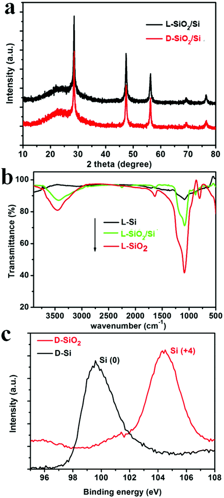 | ||
| Fig. 1 (a) The XRD patterns of reduced SiO2 (SiO2/Si) obtained under 600 °C; (b) the FTIR spectra of L-SiO2, L-SiO2/Si, and L-Si; (c) Si 2p XPS spectra of D-SiO2 and D-Si. | ||
The nano/micro-structures and morphologies were revealed by TEM analyses. From the TEM images, we can see that there are no particular chiral outward shapes for the powders of the D- (Fig. 2a–d, left) and L-forms (Fig. 2a–d, right) in the products of every step. This is quite different to the common helical silica systems in which morphologies with a mirror relationship are always observable for the L- and D-entities. The initial PEI/D-tart@SiO2 hybrids mainly appeared as nanofibers with an average diameter of about 10 nm. After calcination at 800 °C under air to remove the organic components, the as-formed D-SiO2 still showed a similar morphology to that of PEI/D-tart@SiO2, suggesting the highly thermal-resistant stability of the structures. However, the morphology was destroyed after reduction by Mg at 600 °C, and irregular morphologies (including nanoparticles and nano-plates) could be observed. After HF etching, the as-obtained Si products appeared as irregular large nano-plates with sizes of hundreds of nm. During the magnesiothermic reaction, it is possible that the disconnection of Si–O bonds and the formation of Si–Si bonds would result in the fracture of SiO2 nanofibers and the fractured fragments fuse with each other into large plates. The typical HRTEM images of reduced SiO2 (D-SiO2/Si) are also shown in Fig. 2e. Si products with a high degree of crystallization are characterized by the clear and ordered lattice fringes corresponding to (111) faces of cubic-phased Si. Meanwhile, Si with a low degree of crystallization and defects is found according to the disordered lattice fringes (Fig. 2f). Also, the coexistence of well-crystallized and defect-containing Si products was demonstrated in both the L-SiO2/Si and final Si products. These defects are considered to be important for the observed chirality, which will be discussed later.
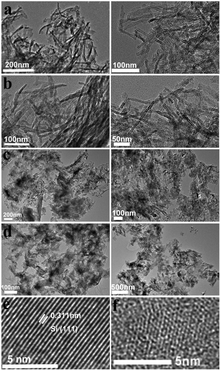 | ||
| Fig. 2 (a–d) TEM images of D-form (left) and L-form (right) products: (a) PEI/D-tart@SiO2 and PEI/L-tart@SiO2, (b) D-SiO2 and L-SiO2, (c) D-SiO2/Si and L-SiO2/Si, and (d) D-Si and L-Si; (e and f) typical HRTEM images of D-SiO2/Si. | ||
To check whether the chirality is transferred to the final Si products, we subjected the samples to the DRCD spectrometer test. As shown in Fig. 3, the DRCD spectra for all of the L- and D-form products showed a typical mirror-image relationship. For the tartaric acids (Fig. 3a), the peaks are around 218 nm, and the L-tart shows a negative signal while the D-tart shows a positive signal. However, when it comes to PEI/L-tart@SiO2 and PEI/D-tart@SiO2 (Fig. 3b), the peak positions are still around 218 nm while the signals are opposite to those of pure chiral tartaric acids. Because there are no characteristic absorption bands in the range of 200–800 nm for SiO2, the chirality can not be directly reflected in the DRCD spectra. However, when achiral chromophores of 2-methylnaphthoquinone (MNQ) were adsorbed on the chiral SiO2, they showed remarkable inductive CD signals in the range of the MNQ absorption band (Fig. 3c), indicating that the chirality of SiO2 can induce optical activity of an achiral guest adsorbed on the chiral silica. After reduction of the chiral SiO2, the SiO2/Si products showed broad CD curves in the range of 300–800 nm, which centred around 400–500 nm and appeared with a mirror relationship for the D- and L-forms. These CD signals were still well preserved in the final Si products after HF etching. It is conclusive that in spite of the destruction of the shape during these steps, the chirality was steadily transferred via two successive modes: firstly from chiral organics to SiO2 and then by self-transfer from SiO2 to Si. The corresponding UV-Vis absorption spectra are also shown in the right column of Fig. 3. For the tartaric acids, they showed strongest absorption in the UV range of 200–230 nm. In the cases of PEI/tart@SiO2, two peaks around 210 nm and 250 nm were present, which are due to tartaric acid and PEI, respectively. The absorption spectra for the SiO2/Si and Si products are also similar, which should be attributed to the presence of Si. Although SiO2/Si and Si showed CD signals in the visible-range, they displayed strong absorption between 200 and 400 nm while their absorption gradually decreased at a longer wavelength from 400 to 800 nm. This is quite different from the common organic substances (e.g., tartaric acids) in which CD peaks are close to their corresponding absorption bands in the UV region. It should be noted here, that to obtain a reliable CD signal, usually, DRCD measurement requires 40 wt% of the samples mixed with KCl, but only about 5 wt% Si powders were enough to get their CD signals.
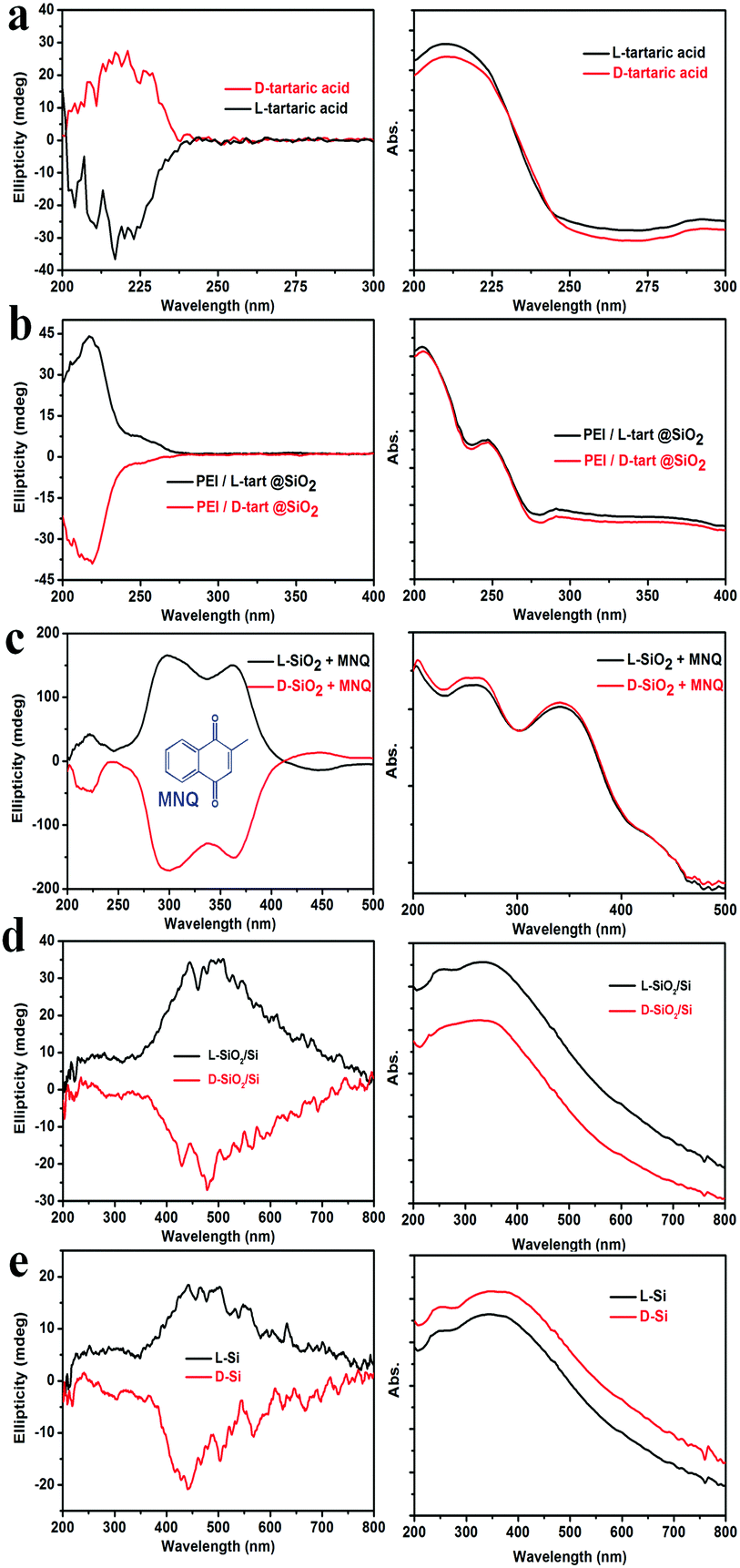 | ||
| Fig. 3 DRCD (left) and corresponding UV-Vis absorption spectra (right) for (a) tartaric acids, (b) PEI/tart@SiO2, (c) SiO2 absorbed with MNQ, (d) SiO2/Si and (e) Si (black lines for L-form while red ones for D-form). | ||
Interestingly, by mixing the chiral Si powders with achiral organic molecules such as polyvinylpyrrolidone K90 (PVP) and trimethoxyphenylsilane (TMPS), we found that chirality induction was promoted from the Si to the residues of PVP or TMPS, as reflected in the vibrational circular dichroism (VCD) and infrared (IR) absorption spectra shown in Fig. 4. It is known that VCD involves the vibrational transitions found in the IR region.1 In the IR spectra, the following peaks were found: in the case of PVP (Fig. 4a), 1660 cm−1 (C![[double bond, length as m-dash]](https://www.rsc.org/images/entities/char_e001.gif) O), 1435 & 1462 cm−1 (C–H), 1290 cm−1 (C–N); in the case of TMPS (Fig. 4b), 1190, 1131, and 1088 cm−1 (Si–O). As shown in the IR spectra of L-Si (Fig. 1b), Si showed no obvious absorption in the range between 850 and 2000 cm−1, and therefore the signals in the IR and VCD spectra in Fig. 4 were mainly attributed to PVP or TMPS. For the L- and D-form products, the IR spectra are nearly identical while the VCD spectra showed a mirror image relationship to the signals at the wavenumbers corresponding to the peaks in the IR spectra, which is indicative of chirality induction. However, for D-Si (or L-Si), the VCD signal for Si-PVP is opposite to that for Si-TMPS (i.e., positive versus negative), which may be related to the difference in the components of the two systems. It is reasonable that for the PVP system, the carbonyl group (CO) may physically interact with the chiral surface of the silicon; in contrast to the TMPS system, in which the methoxyl groups on PhSiOCH3 are hydrolyzed into silanol PhSiOH and then condensed with the silanol groups on the chiral surface of silicon to form a PhSi–O–Si bond, which is chemically modified silicon. Consequently, the strongest intensity of VCD activity with different signs appeared at 1660 cm−1 (CO) and 1088 cm−1 (Si–O) for the PVP- and the TMPS-treated systems, respectively.
O), 1435 & 1462 cm−1 (C–H), 1290 cm−1 (C–N); in the case of TMPS (Fig. 4b), 1190, 1131, and 1088 cm−1 (Si–O). As shown in the IR spectra of L-Si (Fig. 1b), Si showed no obvious absorption in the range between 850 and 2000 cm−1, and therefore the signals in the IR and VCD spectra in Fig. 4 were mainly attributed to PVP or TMPS. For the L- and D-form products, the IR spectra are nearly identical while the VCD spectra showed a mirror image relationship to the signals at the wavenumbers corresponding to the peaks in the IR spectra, which is indicative of chirality induction. However, for D-Si (or L-Si), the VCD signal for Si-PVP is opposite to that for Si-TMPS (i.e., positive versus negative), which may be related to the difference in the components of the two systems. It is reasonable that for the PVP system, the carbonyl group (CO) may physically interact with the chiral surface of the silicon; in contrast to the TMPS system, in which the methoxyl groups on PhSiOCH3 are hydrolyzed into silanol PhSiOH and then condensed with the silanol groups on the chiral surface of silicon to form a PhSi–O–Si bond, which is chemically modified silicon. Consequently, the strongest intensity of VCD activity with different signs appeared at 1660 cm−1 (CO) and 1088 cm−1 (Si–O) for the PVP- and the TMPS-treated systems, respectively.
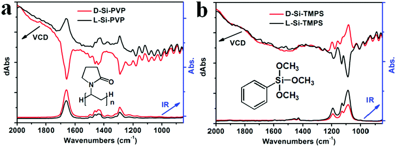 | ||
| Fig. 4 Induced VCD spectra (top) and infrared (IR) spectra (bottom) after introduction of (a) PVP and (b) TMPS onto D-Si (red lines) and L-Si (black lines) (insets, the chemical structure of PVP and TMPS, respectively). | ||
Another two experiments were also conducted to further probe the chirality of reduced SiO2. The first one was to measure the liquid state CD spectra of the D-SiO2/Si powder that was dispersed in water by treatment with ultrasonic waves. They still showed remarkable CD activity, but the CD signal was opposite to that in the solid state (Fig. 5a). The UV-Vis absorption spectra of both were similar to each other, indicating the active component is the SiO2/Si powder (Fig. 5b). Therefore, such CD optical reversion should be caused by the different index of refraction of the dispersion media. The second experiment was to prepare Si products under a lower temperature of 500 °C for 6 h. From the XRD patterns (Fig. 6a), it can be seen that the peak intensities of the products were lower than those under 600 °C. The powder of the reduced SiO2 (SiO2/Si) also showed CD activity with similar spectral lines to those of the products obtained under 600 °C but with lower peak intensities (Fig. 6b). In the DRCD comparison, the SiO2/Si powder was dispersed in KCl with a fixed mass ratio of 10%, and we found that the DRCD intensity is positively correlated with the content of chiral components. The TEM image of this sample showed a nanoparticle-agglomerate morphology (Fig. 6c). Despite the difference in their morphologies between the products obtained under 500 and 600 °C, they showed similar CD signals, which demonstrated that the chirality is not dependent upon the outward morphologies, but relates to the adequate defects in crystalline Si. When the temperature was over 600 °C, the products showed higher peak intensities in the XRD pattern, but the CD peak intensity decreased and no obvious peak was observed (data not shown).
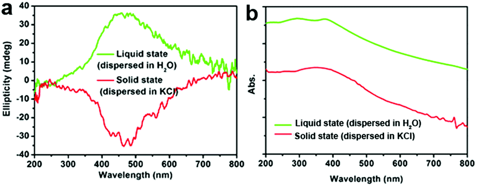 | ||
| Fig. 5 (a) The CD and (b) UV-Vis absorption spectra of D-SiO2/Si powder measured after dispersion in liquid H2O (green line) and solid KCl (red line), respectively. | ||
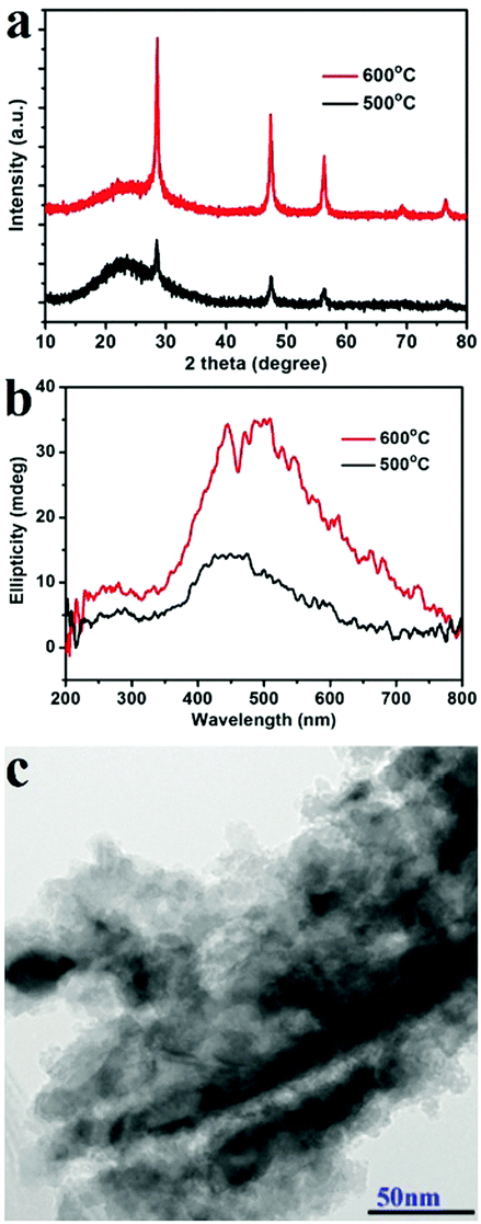 | ||
| Fig. 6 Characterization of the L-SiO2/Si products obtained under 500 °C: (a) XRD, (b) DRCD, (c) TEM images. (For comparison, the XRD and DRCD spectra obtained under 600 °C are also shown as red lines in a and b). | ||
Until now, the detailed reasons for the origin of the chirality in these chiral SiO2 and Si are not yet clear. Generally, chirality can be present across a broad size range: on a small molecular scale, chirality may result from the asymmetric arrangement (e.g., helical conformation, absolute asymmetrical configuration) of a certain number of atoms; on a larger scale, the bottom-up assembly of chiral and/or achiral units may grow into a specific asymmetric shape (e.g., helical shape) and produce shape chirality.6b For the most reported synthetic chiral silica products, they usually appear as electron microscope visualizable helical shapes, which are therefore attributed to the shape chirality.
For those chiral crystalline nanomaterials without helical shapes on the larger length-scale, it is inferred that there is chiral information (e.g., defects, asymmetric crystal faces) on a local and smaller length-scale. For example, semiconductor quantum dots stabilized with achiral ligands showed CD activity, which was considered to be caused by the possible presence of dislocations or point defects.6g These defects mean that the arrangement of atoms in a local domain is symmetry-breaking. According to disordered lattice fringes on the HRTEM image in Fig. 2f, there are nanosized and poorly-crystallized Si products with the possible existence of defects. As mentioned above, the CD signal intensity firstly increased with the temperature rising from 500 to 600 °C and then decreased greatly when the temperature went above 600 °C. Meanwhile, the XRD signal intensity showed a continuous increase, which implied that the crystallinity improvement was due to the reduction in defects. Moreover, the highly symmetrical crystal structure of the cubic-phased Si does not favour chirality. As seen in the TEM images without typical chiral shapes, the defects formed in a suitably low-temperature range should be closely related to the observed CD activity in these chiral Si products. However, at present the chiral arrangement of a certain amount of Si atoms around the molecular-scale hidden in these defects can’t be revealed just by HRTEM images with disordered/distorted lattice fringes, therefore further experimental analysis on the atomic/molecular-scale is needed.
Another important aspect of this chiral transfer is how the defects are produced, thus the unique chiral structure of the chiral SiO2 sources should be discussed. We suppose that the complexes consisting of PEI and chiral tartaric acids (tart) have a helical conformation with tart residues arranged along the PEI axis and thus the silica frame itself forms remembering the asymmetric conformation. As supporting evidence of this model, experimental results show that silica sols, with an average size of 7 nm (Fig. 7a), obtained via the hydrothermal reaction of the bundles of the chiral silica nanofibers (performed at approximately 200 °C, the details of the reaction will be published elsewhere), exhibited remarkable VCD activity (see Fig. 7b). We found that most of the chiral silica powder disappeared after hydrothermal reaction for 5 h after which the reaction solution became transparent. A slightly diluted solution was subjected to TEM analysis, from which we found a clear worm-like network structure self-aggregated from a large amount of sols (nanoparticles). On the other hand, the sol solution was used for drop casting on silicon wafer and subjected to VCD measurement. Very interestingly, both the D and L-form sols in the casting film showed remarkable VCD activity with a mirror relationship in the Si–O stretching vibration range of 1000–1200 cm−1. This means that chiral domains in the silica developed by PEI/tart exist in a space smaller than 7 nm and could self-template the chiral transfer to the corresponding silicon structure. It is known that the chirality of quartz is based on the helical arrangement (with a helix pitch less than 1 nm) of SiO4 tetrahedra with certain deviation of Si–O bond length from a regular tertrahedron.2d In addition, the characterization of some chiral zeolites is based on the building units of a TO4 (T = Si, Al) tetrahedron which chirally deviate from an ideally symmetric tetrahedron.2e Although it is difficult to show the detailed molecular-level structures of our chiral SiO2, it would be conceivable that a certain number of SiO4 tetrahedra are helically arranged into molecular-scale helixes or that spatial distortion occurs on SiO4 tetrahedra in the chiral domains (see the domains marked with red ellipses in Scheme 2c; however, it should be noted that the shown schematic models of the Si–O–Si (or Si–Si) network do not provide or represent real information about Si–O–Si (or Si–Si) bonds such as the lengths, angles and numbers of bonds). During the reduction process of SiO2 (see the part within a rectangular box in Scheme 2c), the oxygen atoms in the bonds of Si–O–Si are removed by the sublimated Mg atoms to form MgO, and then Si–Si bonds are formed in situ and arranged by recalling the structural information of the original Si–O clusters from which Si crystals grow with accompanying formation of chiral defects. The asymmetric atomic array of Si–O–Si provides spatial regulation for the formation of the specific defects of the Si–Si arrangement, and as a result, the initially local chiral information of SiO2 is transferred to the final Si products via the as-proposed self-transfer way. No wonder all the products including the nano-structured hybrids of PEI@SiO2 templated only by PEI (no chiral tart), its calcined form as nanofibrous SiO2 as well as its final reduced form as nano Si did not show chiroptical properties in their CD spectra (data not shown). As a result, the different CD signals among D-Si, L-Si and achiral Si demonstrated that the spatially structural Si–O clusters regulate the final structures of Si–Si with or without chiral defects. However, more experimental observation and theoretical simulations are needed to clarify the specific structures of chiral SiO2 and the Si products and also the chiral transfer mechanism between them in the future.
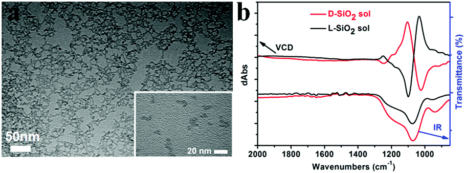 | ||
| Fig. 7 The SiO2 sols transformed from the SiO2 nanofibers after hydrothermal treatment. (a) TEM image from a slightly diluted L-form of SiO2 sol (inset, a high-magnification TEM image taken from a highly diluted SiO2 sol-containing solution); (b) VCD spectra (top) and infrared (IR) spectra (bottom) for D-form (red lines) and L-form (black lines) SiO2 sols. | ||
Conclusions
In summary, this research offers a novel asymmetric chemical synthesis for a solid–solid transformation with the potential of large-scale production of chiral Si nanomaterials. This method used abundant SiO2 raw materials, which were formed under the guidance of PEI polymer templates and endowed with the chirality from tartaric acids. More importantly, the chirality of nanostructured Si is self-transferred from chiral SiO2 sources, which affords a novel way for chirality transfer in order to discuss the origin of chirality/transfer mechanisms and also for designing new chiral inorganic nanomaterials with potential applications in multiple areas such as enantioselective organic synthesis and optical materials.Acknowledgements
This work was supported in part by the MEXT-Supported Program for the Strategic Research Foundation at Private Universities: “Creation of new fusion materials by integration of highly-ordered nano inorganic materials and ultra-precisely controlled organic polymers” (2013–2017) and by JSPS KAKENHI Grant Number JP16H06515 (Coordination Asymmetry).References
-
Comprehensive Chirality, ed. E. M. Carreira and H. Yamamoto, Elsevier, 2012 Search PubMed
.
-
(a) C. Dryzun and D. Avnir, Chem. Commun., 2012, 48, 5874–5876 RSC
-
(a) C. Chen, H. Shi and G. Zhao, J. Phys. Chem. C, 2014, 118, 12041–12049 CrossRef CAS
-
(a) R. M. Hazen and D. S. Sholl, Nat. Mater., 2003, 2, 367–374 CrossRef CAS PubMed
-
(a) B. Frank, X. Yin, M. Schäferling, J. Zhao, S. M. Hein, P. V. Braun and H. Giessen, ACS Nano, 2013, 7, 6321–6329 CrossRef CAS PubMed
-
(a) A. Ben-Moshe, A. O. Govorov and G. Markovich, Angew. Chem., Int. Ed., 2013, 52, 1275–1279 CrossRef CAS PubMed
-
(a) S. D. Elliott, M. P. Moloney and Y. K. Gun'ko, Nano Lett., 2008, 8, 2452–2457 CrossRef CAS PubMed
-
(a) S. Che, Z. Liu, T. Ohsuna, K. Sakamoto, O. Terasaki and T. Tatsumi, Nature, 2004, 429, 281–284 CrossRef CAS PubMed
-
(a) G. Chu, W. Xu, D. Qu, Y. Wang, H. Song and Y. Xu, J. Mater. Chem. C, 2014, 2, 9189–9195 RSC
-
(a) Y. Duan and S. Che, Chem. – Eur. J., 2013, 19, 10468–10472 CrossRef CAS PubMed
- T.-D. Nguyen, J. A. Kelly, W. Y. Hamad and M. J. MacLachlan, Adv. Funct. Mater., 2015, 25, 2175–2181 CrossRef CAS
-
(a) G. P. Lopinski, D. J. Moffatt, D. D. M. Wayner, M. Z. Zgierski and R. A. Wolkow, J. Am. Chem. Soc., 1999, 121, 4532–4533 CrossRef CAS
-
(a) H. Matsukizono and R.-H. Jin, Angew. Chem., Int. Ed., 2012, 51, 5862–5865 CrossRef CAS PubMed
- X. Liu, Y. Gao, R. Jin, H. Luo, P. Peng and Y. Liu, Nano Energy, 2014, 4, 31–38 CrossRef CAS
Footnote |
| † This work was previously filed as patent priority application of JP on Oct. 2014. |
| This journal is © The Royal Society of Chemistry 2017 |