
Rapid open-air deposition of uniform, nanoscale, functional coatings on nanorod arrays†
K. P.
Musselman
 *a,
D.
Muñoz-Rojas
b,
R. L. Z.
Hoye
cd,
H.
Sun
e,
S.-L.
Sahonta
c,
E.
Croft
c,
M. L.
Böhm
d,
C.
Ducati
c and
J. L.
MacManus-Driscoll
c
*a,
D.
Muñoz-Rojas
b,
R. L. Z.
Hoye
cd,
H.
Sun
e,
S.-L.
Sahonta
c,
E.
Croft
c,
M. L.
Böhm
d,
C.
Ducati
c and
J. L.
MacManus-Driscoll
c
aDepartment of Mechanical and Mechatronics Engineering, University of Waterloo, 200 University Ave. West, Waterloo, N2L 3G1, Canada. E-mail: kevin.musselman@uwaterloo.ca
bLaboratoire des Matériaux et du Génie Physique, Université Grenoble-Alpes, CNRS, 3 Parvis Louis Néel, 38016 Grenoble, France
cDepartment of Materials Science and Metallurgy, University of Cambridge, 27 Charles Babbage Road, Cambridge, CB3 0FS, UK
dDepartment of Physics, University of Cambridge, Cavendish Laboratory, JJ Thomson Avenue, Cambridge, CB3 0HE, UK
eIstituto Italiano Di Tecnologia, Via Morego, 30, Genova, 16163, Italy
First published on 11th January 2017
Abstract
Coating of high-aspect-ratio nanostructures has previously been achieved using batch processes poorly suited for high-throughput manufacturing. It is demonstrated that uniform, nanoscale coatings can be rapidly deposited on zinc oxide nanorod arrays in open-air using an atmospheric pressure spatial deposition system. The morphology of the metal oxide coatings is examined and good electrical contact with the underlying nanorods is observed. The functionality of the coatings is demonstrated in colloidal quantum dot and hybrid solar cells.
Conceptual insightsHigh-aspect-ratio nanostructures are critical for many emerging technologies. To improve their functionality, hierarchical coatings are commonly applied to their surfaces using wet-chemistry and vacuum-based batch processes, which have limited throughput. We demonstrate that an atmospheric pressure spatial deposition system can be used to rapidly deposit uniform, nanoscale coatings on nanorod arrays in open air. A variety of metal oxide coatings are deposited on nanorod arrays and characterized. Originally conceived for flat substrates, it was not known whether atmospheric pressure spatial deposition (based on alternating flows of precursor gases) would facilitate conformal coating of high-aspect-ratio nanostructures, particularly when high deposition rates, which include some chemical vapour deposition, are employed. Good electrical contact is observed between the coating and nanorod and functionality is demonstrated in colloidal quantum dot and hybrid solar cells. To our knowledge, this is the first demonstration of a rapid, open-air technique for the scalable deposition of coatings uniformly conformal to high-aspect-ratio nanostructures. This marks an important conceptual shift in the degree of surface engineering and the complexity of nanoscale devices that can be conceived for inexpensive mass-production. Unlike batch processes, this technique can ultimately be combined with established high-throughput (roll-to-roll compatible) methods like gravure and inkjet printing. |
Introduction
Hierarchical nanostructures with large surface areas are critical for emerging technologies in energy generation,1 energy storage,2–8 catalysis & filtration,1,9,10 sensing,1 and functional coatings11 among others. For these applications, hierarchical coatings are commonly applied to the surfaces of high-aspect-ratio nanostructures using wet-chemistry-based1,3–5,9–12 and vacuum-based13–16 batch processes to improve their functionality. As discussed by Liddle et al., the economic viability of a commercial nanotech product ultimately depends on the product of its value and production capacity.17 Traditional vacuum and batch processes for producing hierarchical nanostructures are characterized by limited throughput, and therefore industrially-scalable methods for coating nanostructures are urgently required.Atmospheric pressure spatial atomic layer deposition (AP-SALD) is an emerging technique for the rapid deposition of engineered coatings with atomic-scale thickness control.18–21 In contrast to conventional ALD, which separates reactive precursors in time via successive exposure and purging cycles, often in a vacuum chamber, SALD separates the precursors in space and moves the substrate between the different precursors, which are being supplied constantly, to reproduce the sequential exposure steps. Its ability to quickly deposit thin films over large areas at modest temperatures (typically 100 to 350 °C) makes it very promising for next-generation, low-cost electronic devices and plastic electronics. AP-SALD is a particular variant of SALD that operates at atmospheric pressure and does not require a deposition chamber, is roll-to-roll compatible, and is more than an order of magnitude faster than conventional ALD.18–21 AP-SALD was conceived for depositing thin films on flat substrates, and recently AP-SALD systems have been used to produce films for a variety of traditional and next-generation devices including photovoltaics,22–33 light-emitting diodes,34,35 and transistors.36–39 Many of these reports used chemical vapour deposition conditions (AP-CVD) to deposit the flat films, where some mixing of the precursors occurs in the gas-phase and the growth rate scales linearly with the precursor dosage. AP-CVD conditions are attractive for device production as higher deposition rates are obtained, while still producing smooth, pinhole-free films at modest temperatures, with thicknesses proportional to the number of cycles. However, it is not known whether an atmospheric pressure spatial deposition system will facilitate conformal coating of high-aspect-ratio nanostructures, particularly at higher deposition rates that are required for high-throughput nanomanufacturing. Hence, this is an important topic to study. Furthermore, if these systems prove to be capable of depositing conformal coatings on high-aspect-ratio nanostructures, ideally using high deposition rates, further questions arise: are the properties of the coatings similar to those of previously-studied flat films, and is good electrical contact achieved between the coatings and underlying nanostructures? Answers to these questions are critical to allow scalable production of hierarchical nanostructures for next-generation devices.
In this work, we produce disordered ZnO nanorod arrays and explore the use of an atmospheric pressure spatial deposition system to coat the nanostructures with a variety of metal oxides. We show, for the first time, that such a system is capable of conformally coating high-aspect-ratio nanostructures to produce engineered interfaces in an ambient environment, even when faster chemical vapour deposition (AP-CVD) conditions are employed. The morphology of the coatings is compared to that of previously reported flat films and the electron transfer between the coatings and underlying nanorods is examined. To demonstrate their quality, high-aspect-ratio coatings are employed in nanorod solar cells (hybrid organic–inorganic and colloidal quantum dot) as charge recombination barriers.
Results and discussion
ZnO nanorods were grown on glass substrates coated with indium-tin-oxide (ITO) using the hydrothermal and electrochemical methods detailed in Section S1 of the ESI.† The nanorod arrays were coated with Al2O3, Cu2O, ZnO, nitrogen-doped ZnO (N-doped ZnO), and zinc magnesium oxide (Zn1−xMgxO) layers using a close-proximity atmospheric pressure spatial deposition system discussed previously.18–20 All arrays consisted of nanorods with a variety of orientations. The nanorods coated with Al2O3 and Cu2O were grown electrochemically and the largest nanorods in these arrays were approximately 600 nm long and 60 to 70 nm in diameter. Analysis of cross-sectional TEM images indicated an aspect ratio of 8 ± 2 for the nanorods. This represents a lower bound, as the nanorods are not oriented vertically, such that their lengths are underestimated in the analysis. The nanorods coated with ZnO, N-doped ZnO, and Zn1−xMgxO for solar cells were grown hydrothermally to have lengths of approximately 300 nm and 140 nm, for the hybrid and colloidal quantum dot solar cells respectively, which allowed reliable device fabrication (longer nanorods can poke through the light-absorbing layers, producing unwanted electrical shorting).A schematic diagram of the atmospheric pressure spatial deposition system used to coat the nanorods is shown in Fig. 1a. Nitrogen gas is used to bubble liquid precursors and additional nitrogen flows are used to carry the gaseous precursors to parallel channels in a manifold. The parallel channels of the precursor gases are spatially separated by inserting an inert shielding gas (nitrogen) between them and by balancing gas inlet and exhaust flow rates. The substrate was placed 65 ± 10 μm below the manifold, held at a temperature of 150 ± 10 °C, and oscillated back-and-forth repeatedly through the gas channels to replicate the steps involved in atomic layer deposition (ALD) under atmospheric conditions, without an enclosing chamber. The deposition conditions (precursors, substrate oscillation speed, precursor bubbling and flow rates) used to deposit the various materials are summarized in Table S1 in the ESI.†
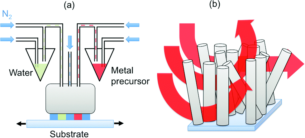 | ||
| Fig. 1 Schematic diagrams of (a) the atmospheric pressure spatial deposition system and (b) the flow of precursor gases through the nanorod arrays. | ||
As this deposition technique relies on the motion of a substrate through alternating flows of precursor gases, complications associated with nanostructured surfaces are expected. Depending on the surface, precursors, flow rate, and substrate velocity, the reactant gas may not be efficiently transported to the entire substrate surface, particularly when randomly oriented high-aspect-ratio nanostructures are present, as illustrated schematically in Fig. 1b. This would result in only partial coating of the nanostructures, such as nanorod arrays. However, previous works on the coating of nanoporous anodic aluminium oxide films with chamber-based SALD at low pressures,40 as well as SALD of micro-scale pillars41 and AP-SALD of macro-scale porous polypropylene fabrics,42 suggest that coating of high-aspect-ratio nanostructures might be possible with an atmospheric pressure spatial deposition system. To verify this, the ZnO nanorods were coated with Al2O3 using the first set of conditions in Table S1 (ESI†). These deposition conditions were selected to ensure isolation of the precursor flows and to provide sufficiently long exposure times to replicate the conditions of conventional ALD. The speed at which the substrate was oscillated between the precursor flows was 2 mm s−1. The Al2O3 coating produced with 40 oscillations is shown in the transmission electron microscopy (TEM) images in Fig. 2a and b. In Fig. 2a, it is seen that the coating is present on multiple nanorods growing in different directions from the ITO substrate. In Fig. 2b, the Al2O3 coating is seen to be extremely conformal on a nanorod up-ended during sample preparation, coating the length of the nanorod uniformly. To our knowledge, this is the first report of conformal coating of high-aspect-ratio nanostructures with an atmospheric pressure spatial deposition system. It is seen that 40 oscillations resulted in a uniform coating thickness of approximately 15 nm. As each oscillation of the substrate under the reactor corresponds to four conventional metal-inert-oxygen ALD cycles, these deposition conditions were found to result in a growth rate of approximately 0.10 nm cycle−1, similar to that reported for conventional ALD of Al2O3.43
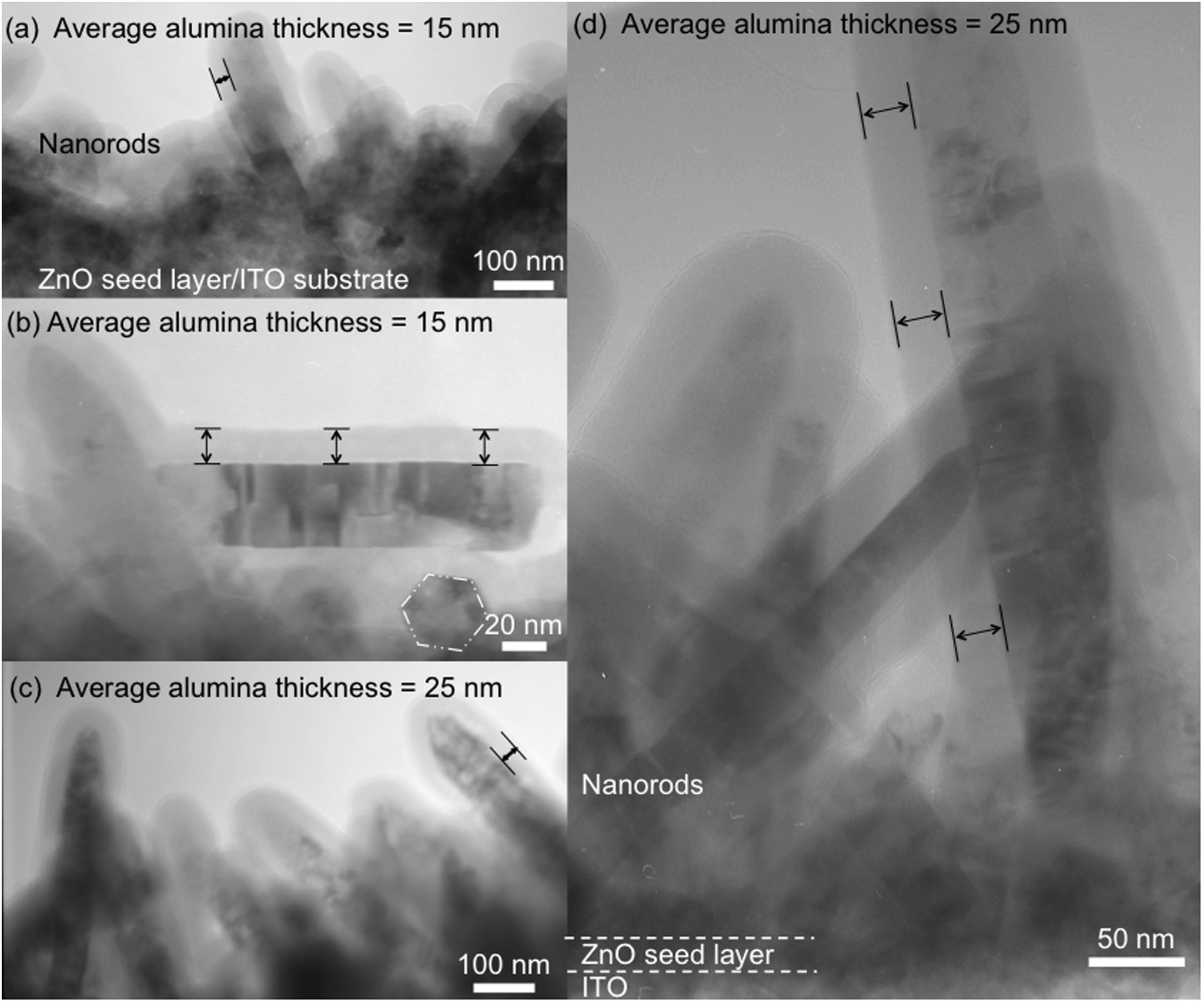 | ||
| Fig. 2 TEM images of ZnO nanorod arrays coated with Al2O3 in (a and b) 25 min and (c and d) 3.5 min. Uniform, nanoscale coatings are seen to extend along the nanorods that are up to 600 nm in length. The hexagonal structure of the nanorods is highlighted in (b) for a nanorod viewed along its length. | ||
To examine whether the conformal coating of high-aspect-ratio nanostructures can be maintained for faster deposition rates more similar to those needed for high-throughput manufacturing, the second set of Al2O3 deposition conditions listed in Table S1 (ESI†) was used. In this case, the speed at which the substrate was oscillated between the precursor flows was increased to 25 mm s−1 from 2 mm s−1. Furthermore, the aluminium and oxygen precursor bubbling rates were twice as high, the nitrogen flow rates carrying the precursors were higher, and the inert nitrogen flow separating the precursors was reduced. The Al2O3-coated ZnO nanorods produced using these conditions are shown in Fig. 2c and d. A 25 nm coating was produced with 60 oscillations, which again corresponds to a growth rate of approximately 0.10 nm cycle−1. The fact that a deposition rate similar to that of conventional ALD was obtained for both sets of deposition conditions suggests that both sets of conditions may achieve ALD growth. A larger range of precursor dosages would need to be investigated to confirm true atomic layer-by-layer deposition. This is not examined here, as the objective is to demonstrate conformal coating of nanostructures at higher deposition rates that are required for high-throughput nanomanufacturing. The coating was very conformal again, covering the entire length of the ZnO nanorods uniformly. Fig. 2d shows a uniform 25 nm Al2O3 coating along a vertically aligned nanorod over 500 nm in length. In contrast, when Sharma et al. coated high-aspect-ratio anodic alumina templates by chamber-based SALD,40 they did not obtain uniform coatings for small nanopore diameters or short exposure times, which could be attributed to gaseous precursor transport and reaction kinetics limiting the film growth. The uniform coatings obtained here suggest that the exposure time (as defined by the substrate oscillation speed) and the geometry of the nanorods were such that a similar growth-limited regime was not reached, despite the rapid deposition rate. Notably, while approximately 25 minutes were required to deposit the 15 nm coating at an oscillation speed of 2 mm s−1, only 3.5 minutes were required to deposit the equally conformal 25 nm coating in Fig. 2c and d over a deposition area of several square inches (oscillation speed of 25 mm s−1). The ability to rapidly deposit thicker coatings with identical uniformity is very promising for the scalable fabrication of large-area devices.
To confirm whether conformal coatings can be produced on the nanorod arrays using AP-CVD conditions, we deposited Zn1−xMgxO and N-doped ZnO on the ZnO nanorods using the deposition conditions detailed in Table S1 (ESI†). These conditions are known to result in CVD growth and hence higher deposition rates (up to 1 nm cycle−1cf. 0.1 nm cycle−1 for Al2O3), as reported previously.19Fig. 3 shows the scanning electron microscopy (SEM) images of pristine ZnO nanorods, as well as those coated with Zn1−xMgxO and N-doped ZnO by AP-CVD (with 40 and 8 oscillations respectively). Again, the morphology of the nanorods is maintained after coating, with no observable clustering or deformation. The presence of Mg in the Zn1−xMgxO coating was confirmed by energy-dispersive X-ray (EDX) spectroscopy measurements (Section S2 in the ESI†). Similar deposition conditions were previously shown to result in a composition of approximately Zn0.54Mg0.46O.19 While a nitrogen peak could not be observed in the EDX spectrum of the N-doped ZnO due to the overlapping O peak, the presence of nitrogen was previously confirmed by X-ray photoelectron spectroscopy for films deposited in a similar manner using the same system.27 These results indicate that conformal coating of high-aspect-ratio nanostructures can similarly be achieved when faster AP-CVD conditions are used.
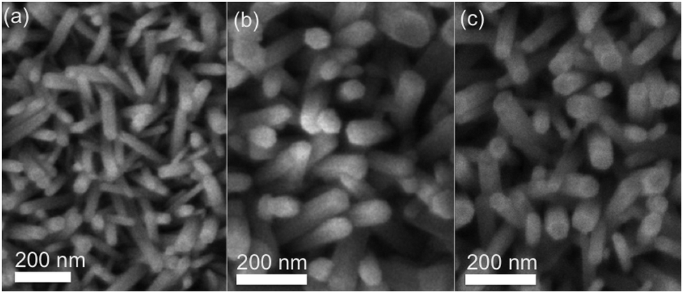 | ||
| Fig. 3 SEM images of ZnO nanorod arrays (a) before coating, and with uniform AP-SALD coatings of (b) Zn1−xMgxO and (c) N-doped ZnO. | ||
While detailed characterization of the various nanoscale coatings is beyond the scope of this communication, it is instructive to know whether the morphology of the coatings is similar to that observed in planar films deposited with the atmospheric pressure spatial deposition system. The system employed in this work has been used previously to produce ZnO thin films on flat substrates. Smooth, polycrystalline films without pinholes or discontinuities were observed for the deposition of ZnO, N-doped ZnO, and Zn1−xMgxO on glass and ITO-glass substrates.19,27–29,44 Similar roughness and sub-100 nm grain size were observed for the ZnO and doped variants, where the grain size varied with deposition temperature. Fig. 4a and b show the TEM images of the ZnO nanorods coated in this work with (a) ZnO and (b) N-doped ZnO. Although the coatings were observed to be continuous in the SEM images in Fig. 3a–c, granular growth is observed in the TEM images, consistent with the previously reported polycrystalline flat films. Past SEM and TEM analysis of Cu2O thin films deposited on flat glass substrates by AP-CVD also revealed a fine-grained structure, where three-dimensional nucleation produced columnar grains that coalesced to form a dense film.45 This phenomenon is not unique to atmospheric pressure spatial deposition, as granular/island-type nucleation has previously been observed for conventional ALD of some materials.46,47 The TEM image in Fig. 4c shows a thin Cu2O coating deposited on ZnO nanorods in this work using a substrate oscillation speed of 10 mm s−1. The nucleation of Cu2O grains on the single crystal nanorods is clearly visible, indicating a similar growth mechanism as for deposition on flat substrates. In both Fig. 4a and c, the granular structure of the ZnO and Cu2O coatings is seen to extend several hundred nanometers along the viewable length of the nanorods. Fig. 4d shows a thicker Cu2O deposition achieved with 2000 cycles at an oscillation speed of 50 mm s−1. The thickness of the coating was estimated to be approximately 50 nm, based on the SEM images and previously reported growth rates for Cu2O deposited by AP-CVD.45 An increased surface roughness was observed (compared to the pristine nanorods in Fig. 3a) but the high-aspect-ratio and hexagonal structure of the nanorods is still clearly visible. As for the previously reported flat Cu2O films, the nanoscale Cu2O nucleations coalesce to form a continuous coating on the surface of the nanorods. Thus, while the deposition substrate in this work (ZnO nanorods) is different than for previous depositions on flat substrates, these results indicate that the atmospheric pressure spatial deposition system can produce coatings with a similar morphology that are conformal to a nanostructured substrate.
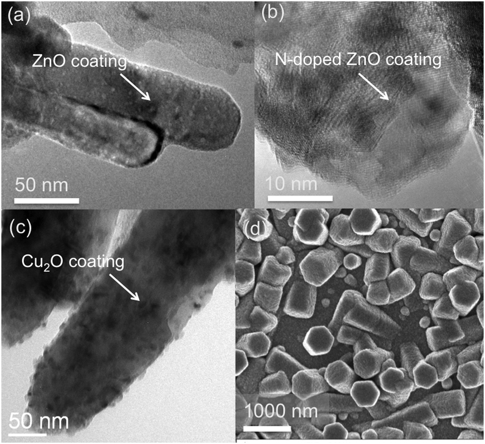 | ||
| Fig. 4 TEM images of ZnO nanorods coated with (a) ZnO, (b) N-doped ZnO, and (c) Cu2O. Nanocrystalline grains are visible on the surfaces of the nanorods. (d) SEM image of ZnO nanorods coated with approximately 50 nm of Cu2O using 2000 cycles. The surface of the nanorods is rougher than the uncoated nanorods shown in Fig. 3a, but the hexagonal geometry of the nanorods is still clearly visible. | ||
If these coatings are to be employed in next-generation devices, it is essential to know whether good electrical contact is achieved between the coating and the underlying nanostructure. To examine this, the photoluminescence spectrum of Zn1−xMgxO-coated nanorods was measured. Fig. 5 shows the normalized photoluminescence spectra of uncoated ZnO nanorods, a Zn1−xMgxO thin film, and ZnO nanorods coated with Zn1−xMgxO. The absolute emission from the Zn1−xMgxO film is an order of magnitude lower than that from the nanorods, due to the smaller volume. As expected, the emission from the Zn1−xMgxO is seen to occur at a higher energy (3.45 eV) than for the ZnO nanorods (3.3 eV), due to the upwards shift of the conduction band (and corresponding increase in bandgap) caused by Mg incorporation.28 When a comparable Zn1−xMgxO film was coated onto the ZnO nanorods however, the photoluminescence spectrum was identical to that of the pristine nanorods, as shown in Fig. 5. The coated nanorods showed no shoulders in their photoluminescence spectra. Thus the coated nanorods emit predominantly from the underlying ZnO, despite the fact that the Zn1−xMgxO is present on the surface where the optical excitation is incident. This may be because the optically excited charges in the Zn1−xMgxO are readily injected into lower-lying energy levels in the underlying ZnO nanorods (i.e. the ZnO nanorods quench the emission from the coating). This behaviour is advantageous in applications such as photovoltaics and photocatalysis, where the transport of electrons away from a charge-separating interface is desired. Furthermore, this behaviour indicates that excellent electrical contact is achieved between the nanorods and the coating.
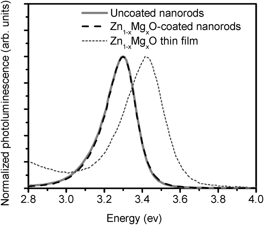 | ||
| Fig. 5 Photoluminescence spectra of pristine ZnO nanorods, a Zn1−xMgxO thin film, and ZnO nanorods coated with Zn1−xMgxO. | ||
The ability of these coatings to engineer the functionality of nanostructured device interfaces was confirmed by employing the ZnO nanorods coated with ZnO, N-doped ZnO, and Zn1−xMgxO in prototype colloidal quantum dot solar cells and oxide–polymer hybrid cells. Schematic diagrams of the solar cell architectures are shown in Fig. 6a and b. Based on previous studies of nanorod/nanowire solar cells, the nanorods are expected to increase absorption by scattering incident light and reduce the distances that minority electrons in the PbSe quantum dots and excitons in the poly(3,4-ethylenedioxythiophene) (P3HT) have to travel to reach the electron-accepting ZnO.48–52 The average performance parameters for the colloidal quantum dot solar cells with different coatings deposited using the AP-SALD system are summarized in Table 1. The bandgap of the PbSe quantum dots was measured to be 1.51 eV (Section S3 of the ESI†).
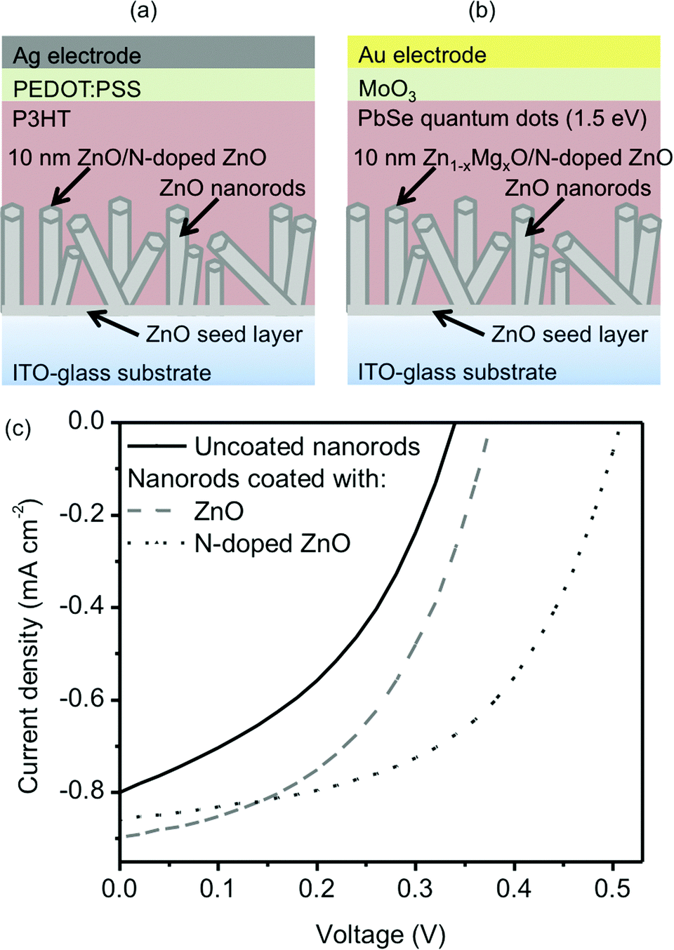 | ||
| Fig. 6 Schematic illustrations of (a) a ZnO nanorod–P3HT hybrid solar cell and (b) a ZnO nanorod–PbSe colloidal quantum dot solar cell with thin (less than 10 nm) ZnO, Zn1−xMgxO, and N-doped ZnO coatings on the nanorods. (c) Current density–voltage measurements of ZnO nanorod–P3HT hybrid cells with ZnO, N-doped ZnO, and no coating. All measurements were performed under simulated AM1.5G solar illumination. | ||
| ZnO nanorod coating | Open-circuit voltage (V) | Short-circuit current density (mA cm−2) | Power conversion efficiency (%) |
|---|---|---|---|
| None | 0.41 ± 0.06 | 5.6 ± 0.9 | 0.6 ± 0.2 |
| Zn0.54Mg0.46O | 0.45 ± 0.06 | 6 ± 1 | 0.7 ± 0.2 |
| N-doped ZnO | 0.46 ± 0.02 | 8 ± 1 | 0.9 ± 0.2 |
| N + Zn0.54Mg0.46O | 0.52 ± 0.02 | 4.9 ± 0.8 | 0.6 ± 0.1 |
Coating the ZnO nanorods with Zn0.54Mg0.46O resulted in an increase in the average open-circuit voltage from 0.41 V to 0.45 V. This is consistent with previous work employing Zn1−xMgxO thin films made using the atmospheric pressure spatial deposition system in flat colloidal quantum dot solar cells, where it was shown that placing Zn1−xMgxO at the interface with the quantum dots improved the open-circuit voltage of the cells via an optimized energy level alignment.28 Coating the nanorods with N-doped ZnO resulted in an increase in the average short-circuit current density of the colloidal quantum dot cells from 5.6 mA cm−2 to 8 mA cm−2. This is consistent with previous work using AP-CVD N-doped ZnO thin films in flat hybrid polymer–oxide solar cells, where it was shown that placing N-doped ZnO at the interface with the polymer improved charge separation via a light-activated detrapping process on the oxide surface.27 Interestingly, in this work, the N-doped ZnO coating was also observed to increase the average open-circuit voltage of the colloidal quantum dot cells to 0.46 V. It is expected that the inclusion of nitrogen dopants in the ZnO coating will result in impurity scattering and lower electron mobility in the coating, as compared to the single crystal nanorod. Furthermore, it is expected that a shell material with lower mobility would confine electrons to the higher-conductivity nanorod core, isolating them from the interface with the quantum dots. This would reduce the recombination of electrons from the ZnO with holes from the PbSe, increasing the open-circuit voltage, consistent with previous reports of reduced recombination and enhanced open-circuit voltages in dye-sensitized and hybrid solar cells employing core–shell nanowires.52–54 The highest open-circuit voltage was observed in the colloidal quantum dot cells when both magnesium and nitrogen were incorporated in the AP-CVD ZnO coating, but this was accompanied by a significant reduction in the short-circuit current density. It is possible that introducing both magnesium and nitrogen may have significantly reduced the carrier mobility of the coating, which again prevented interfacial recombination, but may also have hindered transport of electrons from the PbSe quantum dots to the nanorod cores, thus limiting the extractable photocurrent. This behavior has been observed previously when insulating Al2O3 shell layers were used in nanowire dye-sensitized solar cells.54 The conformal nature of the depositions demonstrated here is also advantageous in that the coatings are expected to cover any shunt pathways that exist at the base of the nanorods (i.e. exposed ITO), which would also prevent recombination in the devices. The reduction in recombination current achieved with the coatings was evident in dark current density measurements of the nanorod colloidal quantum dot solar cells (Section S4 of the ESI†).
The performance of the ZnO nanorod-P3HT solar cells was also found to improve when the coatings were introduced. Fig. 6c shows representative current density–voltage data for the hybrid cells under simulated solar illumination, with and without ZnO and N-doped ZnO AP-CVD coatings on the nanorods. The most significant improvement was the enhancement in open-circuit voltage for the cells with an N-doped ZnO coating. As in the case of the ZnO nanorod–PbSe colloidal quantum dot solar cells, it is possible that the N-doped ZnO acts as a low-mobility shell that confines electron transport to the core, preventing recombination at the oxide–polymer interface, as well as eliminating shunt pathways at the base of the nanorods. Absorption, external quantum efficiency, light-intensity dependent open-circuit voltage, and photovoltage decay measurements were also performed on the hybrid cells (Section S5 in the ESI†) and were consistent with the N-doped ZnO coating acting as a barrier to recombination. The undoped ZnO coating appears to have the same affect in Fig. 6c, but to a smaller extent. A lower mobility in the N-doped ZnO coating is expected to follow from the nitrogen dopant acting as an impurity/scattering center.
The significant increases in open-circuit voltage and reduction in dark current density observed when the coatings were introduced into the solar cells clearly demonstrate the uniform, continuous nature of the nanoscale coatings. If the coatings were not conformal, recombination pathways would remain between the light absorbing materials (PbSe colloidal quantum dots and P3HT) and the ZnO nanorod cores or substrate, such that these improvements would not be expected.
Conclusions
Nanoscale coatings of ZnO, N-doped ZnO, Zn1−xMgxO, Cu2O, and Al2O3 were deposited on ZnO nanorods using an atmospheric pressure spatial deposition system. It was shown that complete coverage of the high-aspect-ratio nanorods could be achieved with the various coating materials using conditions that resulted in deposition rates similar to conventional ALD (AP-SALD), as well as faster AP-CVD conditions. Notably, the conformal coatings could be produced very quickly over large areas (e.g. 25 nm Al2O3 coatings deposited over several square inches in 3.5 min). To our knowledge, this is the first demonstration of a rapid, open-air technique for the scalable deposition of coatings uniformly conformal to high-aspect-ratio nanostructures. The ZnO, N-doped ZnO, and Cu2O coatings were found to consist of nanocrystalline grains, similar to flat films deposited previously under similar conditions. Strong photoluminescence quenching was observed for ZnO nanorods coated with Zn1−xMgxO, indicating that charge transfer between the coating and the nanorod core is very efficient. To test their suitability as functional coatings, ZnO, N-doped ZnO, and Zn1−xMgxO coatings were employed in prototype nanorod hybrid and colloidal quantum dot solar cells. In both cases, the coatings improved the efficiency of the devices, which was attributed to a reduction in unwanted charge recombination at the nanorod–absorber interface, as well as the potential elimination of shunt pathways at the base of the nanorods. While optimization of the nanorod cell fabrication procedures is needed to improve the overall efficiency of the devices, the observed performance improvement demonstrates that nanoscale coatings deposited quickly with an atmospheric pressure spatial deposition system are capable of engineering the functionality of large-area, nanostructured device interfaces. Unlike existing processes for depositing nanostructured coatings, this technique can ultimately be combined with established high-throughput methods like gravure and inkjet printing to realize ubiquitous nanostructured devices.55 This marks an important conceptual shift in the complexity of nanoscale devices that can be conceived for mass-production in an inexpensive manner (i.e. without vacuum, lithographic, or batch processes).Acknowledgements
K. P. M. acknowledges a University of Waterloo startup grant and Girton College (Cambridge). K. P. M. and D. M.-R. acknowledge a University of Waterloo IRPG-EU grant. D. M.-R. and J. L. M.-D. acknowledge the Marie Curie Actions (FP7/2007-2013, Grant Agreement No. 219332 and 631111), and the Ramon y Cajal 2011 programme from the Spanish MICINN and the European Social Fund, and the Comissionat per a Universitats I Recerca (CUR) del DIUE de la Generalitat de Catalunya, Spain. R. L. Z. H. acknowledges the Rutherford Foundation of New Zealand and the Cambridge Commonwealth, European & International Trusts. S.-L. S. acknowledges EPSRC Platform Grant EP/E026206/1. E. C. and C. D. acknowledge the ERC (Grant no. 259619 PHOTO EM) for support with electron microscopy characterization. M. L. B. acknowledges Christs College (Cambridge) and EPSRC (Grant Code EP/G037221/1).References
- J. L. Vivero-Escoto, Y. Chiang, K. Wu and Y. Yamauchi, Sci. Technol. Adv. Mater., 2012, 13, 013003 CrossRef PubMed.
- M. V. Reddy, G. V. S. Rao and B. V. R. Chowdari, Chem. Rev., 2013, 113, 5364 CrossRef CAS PubMed.
- Y. Chen, B. Song, M. Li, L. Lu and J. Xue, Adv. Funct. Mater., 2014, 24, 319 CrossRef CAS.
- R. Chen, T. Zhao, W. Wu, F. Wu, L. Li, J. Qian, R. Xu, H. Wu, H. M. Albishri, A. S. Al-Bogami, D. Abd El-Hady, J. Lu and K. Amine, Nano Lett., 2014, 14, 5899 CrossRef CAS PubMed.
- B. Luo and L. Zhi, Energy Environ. Sci., 2015, 8, 456 CAS.
- Y. Tang, Y. Zhang, W. Li, B. Ma and X. Chen, Chem. Soc. Rev., 2015, 44, 5926 RSC.
- Y. Zhang, Y. Tang, W. Li and X. Chen, ChemNanoMat, 2016, 2, 764 CrossRef CAS.
- G. O. Park, J. Yoon, J. K. Shon, Y. S. Choi, J. G. Won, S. B. Park, K. H. Kim, H. Kim, W.-S. Yoon and J. M. Kim, Adv. Funct. Mater., 2016, 26, 2800 CrossRef CAS.
- X. Liu, Z. Chang, L. Luo, T. Xu, X. Lei, J. Liu and X. Sun, Chem. Mater., 2014, 26, 1889 CrossRef CAS.
- D. J. You, X. Jin, J. H. Kim, S.-A. Jin, S. Lee, K. H. Choi, W. J. Baek, C. Pak and J. M. Kim, Int. J. Hydrogen Energy, 2015, 40, 12352 CrossRef CAS.
- Y. Sohn, D. Kim, S. Lee, M. Yin, J. Y. Song, W. Hwang, S. Park, H. Kim, Y. Kob and I. Han, J. Mater. Chem. A, 2014, 2, 11465 CAS.
- Y. Li and J. Shi, Adv. Mater., 2014, 26, 3176 CrossRef CAS PubMed.
- K. Heo, H. Lee, J. Jian, D.-J. Lee, Y. Park, C. Lee, B. Y. Lee and S. Hong, Nanoscale Res. Lett., 2015, 10, 331 CrossRef PubMed.
- C. Tang, B.-Q. Li, Q. Zhang, L. Zhu, H.-F. Wang, J.-L. Shi and F. Wei, Adv. Funct. Mater., 2015, 26, 577 CrossRef.
- M. Abd-Ellah, S. Bazargan, J. P. Thomas, M. A. Rahman, S. Srivastava, X. Wang, N. F. Heinig and K. T. Leung, Adv. Electron. Mater., 2015, 1, 1500032 CrossRef.
- W. Niu, X. Li, S. K. Karuturi, D. W. Fam, H. Fan and S. Shrestha, Nanotechnology, 2015, 26, 064001 CrossRef CAS PubMed.
- J. A. Liddle and G. M. Gallatin, ACS Nano, 2016, 10, 2995 CrossRef CAS PubMed.
- R. L. Z. Hoye, D. Muñoz-Rojas, S. F. Nelson, A. Illiberi, P. Poodt, F. Roozeboom and J. L. MacManus-Driscoll, APL Mater., 2015, 3, 040701 CrossRef.
- R. L. Z. Hoye, D. Muñoz-Rojas, K. P. Musselman, Y. Vaynzof and J. L. MacManus-Driscoll, ACS Appl. Mater. Interfaces, 2015, 7, 10684 CAS.
- D. Muñoz-Rojas and J. MacManus-Driscoll, Mater. Horiz., 2014, 1, 314 RSC.
- P. Poodt, D. C. Cameron, E. Dickey, S. M. George, V. Kuznetsov, G. N. Parsons, F. Roozeboom, G. Sundaram and A. Vermeer, J. Vac. Sci. Technol., A, 2012, 30, 010802 Search PubMed.
- C. Armstrong, M. Price, D. Muñoz-Rojas, N. Davis, M. Abdi-Jalebi, R. H. Friend, N. Greenham, J. L. MacManus-Driscoll, M. Böhm and K. P. Musselman, ACS Nano, 2015, 9, 11863 CrossRef CAS PubMed.
- R. L. Z. Hoye, R. E. Brandt, Y. Ievskaya, S. Heffernan, K. P. Musselman, T. Buonassisi and J. L. MacManus-Driscoll, APL Mater., 2015, 3, 020901 CrossRef.
- Y. Ievskaya, R. L. Z. Hoye, A. Sadhanala, K. P. Musselman and J. L. MacManus-Driscoll, Sol. Energy Mater. Sol. Cells, 2015, 135, 43 CrossRef CAS.
- S.-Y. Lien, C.-H. Yang, K.-C. Wu and C.-Y. Kung, Nanoscale Res. Lett., 2015, 10, 93 CrossRef PubMed.
- R. L. Z. Hoye, S. Heffernan, Y. Ievskaya, A. Sadhanala, A. Flewitt, R. H. Friend, J. L. MacManus-Driscoll and K. P. Musselman, ACS Appl. Mater. Interfaces, 2014, 6, 22192 CAS.
- K. P. Musselman, S. Albert-Seifried, R. L. Z. Hoye, A. Sadhanala, D. Muñoz-Rojas, J. L. MacManus-Driscoll and R. H. Friend, Adv. Funct. Mater., 2014, 24, 3562 CrossRef CAS PubMed.
- R. L. Z. Hoye, B. Ehrler, M. L. Böhm, D. Muñoz-Rojas, R. M. Altamimi, A. Y. Alyamani, Y. Vaynzof, A. Sadhanala, G. Ercolano, N. C. Greenham, R. H. Friend, J. L. MacManus-Driscoll and K. P. Musselman, Adv. Energy Mater., 2014, 4, 1301544 CrossRef PubMed.
- R. L. Z. Hoye, D. Muñoz-Rojas, D. C. Iza, K. P. Musselman and J. L. MacManus-Driscoll, Sol. Energy Mater. Sol. Cells, 2013, 116, 197 CrossRef CAS.
- A. T. Marin, D. Muñoz-Rojas, D. C. Iza, T. Gershon, K. P. Musselman and J. L. MacManus-Driscoll, Adv. Funct. Mater., 2013, 23, 3413 CrossRef CAS.
- D. Muñoz-Rojas, H. Sun, D. C. Iza, J. Weickert, L. Chen, H. Wang, L. Schmidt-Mende and J. L. MacManus-Driscoll, Prog. Photovoltaics, 2013, 21, 393 Search PubMed.
- B. Ehrler, K. P. Musselman, M. L. Böhm, F. S. F. Morgenstern, Y. Vaynzof, B. J. Walker, J. L. MacManus-Driscoll and N. C. Greenham, ACS Nano, 2013, 7, 4210 CrossRef CAS PubMed.
- P. Poodt, A. Lankhorst, F. Roozeboom, K. Spee, D. Maas and A. Vermeer, Adv. Mater., 2010, 22, 3564 CrossRef CAS PubMed.
- R. L. Z. Hoye, K. P. Musselman, M. R. Chua, A. Sadhanala, R. D. Raninga, J. L. MacManus-Driscoll, R. H. Friend and D. Credgington, J. Mater. Chem. C, 2015, 3, 9327 RSC.
- R. L. Z. Hoye, M. R. Chua, K. P. Musselman, G. Li, M.-L. Lai, Z.-K. Tan, N. C. Greenham, J. L. MacManus-Driscoll, R. H. Friend and D. Credgington, Adv. Mater., 2015, 27, 1414 CrossRef CAS PubMed.
- A. Illiberi, B. Cobb, A. Sharma, T. Grehl, H. Brongersma, F. Roozeboom, G. Gelinck and P. Poodt, ACS Appl. Mater. Interfaces, 2015, 7, 3671 CAS.
- D. H. Levy, S. F. Nelson and D. Freeman, J. Disp. Technol., 2009, 5, 484 CrossRef CAS.
- D. A. Mourey, S. K. Park, D. A. Zhao, J. Sun, Y. V. Li, S. Subramanian, S. F. Nelson, D. H. Levy, J. E. Anthony and T. N. Jackson, Org. Electron., 2009, 10, 1632 CrossRef CAS.
- J. Sun, D. A. Mourey, D. Zhao, S. K. Park, S. F. Nelson, D. H. Levy, D. Freeman, P. Cowdery-Corvan, L. Tutt and T. N. Jackson, IEEE Electron Device Lett., 2008, 29, 721 CrossRef CAS.
- K. Sharma, D. Routkevitch, N. Varaksa and S. M. George, J. Vac. Sci. Technol., A, 2016, 34, 01A146 Search PubMed.
- S. Moitzheim, E. Balder, P. Poodt, S. Unnikrishnan and P. M. Vereecken, ECS Meeting Abstracts, PRiME Meeting, Honolulu, Hawaii, October 2–7, 2016.
- M. M. Mousa, PhD thesis, North Carolina State University, 2015.
- J. W. Elam, M. D. Groner and S. M. George, Rev. Sci. Instrum., 2002, 73, 2981 CrossRef CAS.
- L. Dunlop, A. Kursumovic and J. L. MacManus-Driscoll, Appl. Phys. Lett., 2008, 93, 172111 CrossRef.
- D. Muñoz-Rojas, M. Jordan, C. Yeoh, A. T. Marin, A. Kursumovic, L. A. Dunlop, D. C. Iza, A. Chen, H. Wang and J. L. MacManus Driscoll, AIP Adv., 2012, 2, 042179 CrossRef.
- R. L. Puurunen, W. Vandervorst, W. F. A. Besling, O. Richard, H. Bender, T. Conard, C. Zhao, A. Delabie, M. Caymax, S. De Gendt, M. Heyns, M. M. Viitanen, M. de Ridder, H. H. Brongersma, Y. de Tamminga, T. Dao, T. de Win, M. Verheijen, M. Kaiser and M. Tuominen, J. Appl. Phys., 2004, 96, 4878 CrossRef CAS.
- M. Cassira, F. Goubina, C. Bernaya, P. Vernouxa and D. Lincot, Appl. Surf. Sci., 2002, 193, 120 CrossRef.
- K. P. Musselman, A. Wisnet, D. C. Iza, H. C. Hesse, C. Scheu, J. L. MacManus-Driscoll and L. Schmidt-Mende, Adv. Mater., 2010, 22, E254 CrossRef CAS PubMed.
- J. Jean, S. Chang, P. R. Brown, J. J. Cheng, P. H. Rekemeyer, M. G. Bawendi, S. Gradečak and V. Bulović, Adv. Mater., 2013, 25, 2790 CrossRef CAS PubMed.
- K. S. Leschkies, A. G. Jacobs, D. J. Norris and E. S. Aydil, Appl. Phys. Lett., 2009, 95, 193103 CrossRef.
- J. A. Dorman, J. Weickert, J. B. Reindl, M. Putnik, A. Wisnet, M. Noebels, C. Scheu and L. Schmidt-Mende, J. Phys. Chem. C, 2014, 118, 16672 CAS.
- L. E. Greene, M. Law, B. D. Yuhas and P. Yang, J. Phys. Chem. C, 2007, 111, 18451 CAS.
- N. O. V. Plank, H. J. Snaith, C. Ducati, J. S. Bendall, L. Schmidt-Mende and M. E. Well, Nanotechnology, 2008, 19, 465603 CrossRef CAS PubMed.
- M. Law, L. E. Greene, A. Radenovic, T. Kuykendall, J. Liphardt and P. Yang, J. Phys. Chem. B, 2006, 110, 22652 CrossRef CAS PubMed.
- K. P. Musselman, C. F. Uzoma and M. S. Miller, Chem. Mater., 2016, 28, 8443 CrossRef CAS.
Footnote |
| † Electronic supplementary information (ESI) available: Experimental methods, energy-dispersive X-ray measurements, PbSe quantum dot band-gap measurement, dark current density measurements, and characterization of ZnO nanorod-P3HT solar cells. See DOI: 10.1039/c6nh00197a |
| This journal is © The Royal Society of Chemistry 2017 |