Recent advances in black phosphorus-based photonics, electronics, sensors and energy devices

Ye Zhou a, Maoxian Zhang b, Zhinan Guo c, Lili Miao c, Su-Ting Han d, Ziya Wang b, Xiuwen Zhang d, Han Zhang *c and Zhengchun Peng *b
aInstitute for Advanced Study, Shenzhen University, Shenzhen, 518060, China
bKey Laboratory of Ministry of Education for Optoelectronic Devices and Systems, College of Optoelectronic Engineering, Shenzhen University, Shenzhen, 518060, China. E-mail: zcpeng@szu.edu.cn
cSZU-NUS Collaborative Innovation Center for Optoelectronic Science and Technology, Shenzhen University, Shenzhen, 518060, China. E-mail: hzhang@szu.edu.cn
dCollege of Electronic Science and Technology, Shenzhen University, Shenzhen, 518060, China

Received 16th July 2017 , Accepted 8th September 2017

First published on 8th September 2017


Abstract

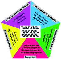
In the past several years, two-dimensional black phosphorus (BP) has captured the research community's interest because of its unique electronic, photonic, and mechanical properties. Remarkable efforts have been made regarding the synthesis, fundamental understanding, and applications of BP in the fields of nanoelectronics, nanophotonics, and optoelectronics. In this review, we summarize the recent developments in the study of BP, which covers the state-of-the-art synthesis methods for preparing single-layer or few-layer BP, the recent advances in characterizing its electronic, optical and mechanical properties, and the reported functional devices utilizing such properties. Finally we discuss the existing challenges in developing BP-based nanoelectronics and optoelectronics, and describe the prospects for future BP-related research.


image file: c7mh00543a-p1.tif

Ye Zhou

Prof. Ye Zhou is an IAS Fellow in the Institute for Advanced Study at Shenzhen University. His research interests include flexible/printed electronics, organic/inorganic semiconductors, surface/interface physics, nanostructured materials and devices for technological applications such as logic circuit, data storage, energy-harvesting, photonics and sensors.

image file: c7mh00543a-p2.tif

Maoxian Zhang

Maoxian Zhang is a MS student in the College of Optoelectronic Engineering at Shenzhen University. His research interests include semiconductor materials, 2D materials, material simulation, and quantum-dot solar cells.

image file: c7mh00543a-p3.tif

Zhinan Guo

Zhinan Guo is an associate research fellow in the International Collaborative Laboratory of 2D Materials for Optoelectronic Science and Technology, Shenzhen University. His research interests include 2D material design and fabrication for optoelectronic applications, interactions between light and 2D materials, and surface enhanced Raman spectroscopy.

image file: c7mh00543a-p4.tif

Han Zhang

Prof. Han Zhang is the director of Shenzhen Engineering Laboratory of Phosphorene and Optoelectronics at Shenzhen University. His current research is on the ultrafast and nonlinear photonics of 2D materials. He is an associate editor of OSA Photonics Research and Editorial Board Member of Scientific Reports, and a lead guest editor of Optical Engineering and Optics Communication.

image file: c7mh00543a-p5.tif

Zhengchun Peng

Prof. Zhengchun Peng is the director of Center for Stretchable Electronics and Nanorobotic Systems at Shenzhen University. His research interests include stretchable electronics, nanosensors, nanoenergy devices, MEMS, microfluidics, and their applications in electronic skin, wearable electronics, environmental energy harvesting, and nanorobotic tools for biomedical research.


1. Introduction

The scientific community has been studying layered materials for more than 150 years.1 Nevertheless, scientists have only just begun to realize the true potential of layered materials for advanced technological applications. Since the discovery of graphene in 2004, research on two-dimensional (2D) materials has become the emphasis of active research in nanotechnology.2,3 The most unique property of 2D materials arises from their distinctive van der Waals structure.4–6 Bulk materials are composed of vertically stacked layers with van der Waals forces as a replacement for covalent bonds. When the thicknesses of these materials are scaled down to a single atomic layer or a few layers, unexpected changes in their physical properties occur.7 Compared to common bulk materials, 2D materials can offer additional benefits such as mechanical flexibility, transparency, robustness, and easy integration. In addition, different 2D materials can be stacked layer-by-layer with van der Waals forces, creating 2D heterostructures and solving the “lattice mismatch” issue, and presenting a flexible methodology for designing materials with desired physical properties for a variety of uses.

Graphene and transition metal dichalcogenides (TMDs) were among the most extensively investigated 2D materials.8,9 Despite the extensive research on the characteristics and applications of graphene and TMDs in nanoelectronics, researchers have been confronted with the following challenges. A graphene transistor cannot be switched off because graphene lacks a bandgap, and the observed mobility of TMD-based devices is relatively low due to the scattering of charge carriers and their heavy effective mass. To mitigate these problems, researchers have attempted to open an electronic band gap and control the interfaces of these 2D materials with other materials,10 however, the on/off current ratio of graphene devices and the mobility of TMD devices still cannot meet the logic requirements of the semiconductor and optoelectronics industries.

Since 2014, black phosphorus (BP), with its moderate and tunable bandgap, has become the new focus of 2D material research.11 It is composed of phosphorus atoms held together by strong bonds, forming layers that interact through weak van der Waals forces. Because of its structure without surface dangling bonds, BP, similar to graphene and TMDs, is able to withstand very large localized deformations without breaking.12,13 As a result, BP can offer a new platform on which flexible nanosystems with novel electronic and optical properties can be attained. In addition, single-layer and few-layer BP are predicted to bridge the bandgap range from 0.3 to 2 eV theoretically, bridging the graphene (zero bandgap) and semiconducting TMDs (bandgaps higher than 1.57 eV). Monolayer and few-layer BP transistors have been successfully demonstrated with a currenton/currentoff ratio of 105 and a mobility of up to 1000 cm V−1 s−1, which is significantly higher than transistors made of TMD. Hence, BP holds potential as a promising semiconducting material for optoelectronic and nanoelectronic devices.

Similar to graphene and TMDs, single-layer or few-layer BP can be obtained by both mechanical and liquid-phase exfoliation.14–16 Other than a suitable bandgap which is tuneable from the visible to mid-infrared, BP has shown many other advantages such as non-toxicity, intrinsic ambipolar behavior, distinctive anisotropy and low thermal conductivity,17,18 which can be utilized to develop functional electronic, photonic, and optoelectronic devices. Another important advantage of the atomically thin 2D BP is its superior resistance to short channel effects at the scaling limit. Therefore, the rediscovery of this new 2D layered material with a single element that can be applied in the semiconductor industry, has attracted the interest of chemists, physicists, material scientists and engineers from numerous research areas.

This review provides an overview of the development of state-of-the-art BP-based electronic, photonic, and optoelectronic devices. Fig. 1 illustrates the relationship among the different sections of this review. Firstly, we supplement the concrete knowledge about the structure of BP and existing fabrication techniques for monolayer or few-layer BP, which forms the foundation for the characterization of its unique properties. Then, we focus on ways to modify the photonic, electronic, and optoelectronic properties of BP, and discuss the advances in applying BP in novel devices, including optical absorbers, modulators, detectors, field-effect transistors, memory, sensors, and energy devices. Furthermore, we describe the existing challenges including the major issues of material degradation encountered in realizing BP-based devices, and examine the creative efforts to address this issue. Finally, we conclude with our perspective on the future research direction in advancing BP-based devices.


image file: c7mh00543a-f1.tif
Fig. 1 Schematic illustration of the relationship among different sections in this review.

2. Structure and fabrication of BP

2.1 Structure of BP

Unlike other kinds of phosphorus allotrope, BP is the only one that is stable to high temperature and in the form of a 2D layer structure like graphene and TMDs.19 The building block of BP is an atomic layer with long-range periodicity. Within each layer of BP, each sp3 phosphorus atom is covalently bonded to three neighbouring phosphorus atoms at 2.18 Å with one lone pair of electrons, forming a structure of a quadrangular pyramid. Two of the three neighbouring phosphorus atoms are in the plane of the layer at 99° from one another, and the third lies between the layers at 103°, creating an average angle of 102°,20 and forming a puckered honeycomb BP layer, as shown in Fig. 2a, which results in anisotropy in its various optical properties,21–24 mechanical properties,25–28 thermo electronic properties,29 electrical conductance,30 and Poisson's ratio along the x and y directions.31,32 In the z direction, many BP layers are stacked under van der Waals interactions, forming a BP crystal. The distance between the two layers is around 5 Å.33 Anisotropy is due to the two arrangements of zigzag and armchair in the different directions. Lau's and Ji's groups cooperatively reported the obviously anisotropic vibration response of ultrathin black phosphorus in the tensile state.34 Their studies found that the typical optical vibrations of ultrathin black phosphorus present distinct responses under two tensile directions. And the response in the zigzag direction has the highest change efficiency, which is far beyond that of other two-dimensional materials. Some theoretical studies have implied that this anisotropic response is derived from the change of bond length and bond angle of phosphorus atoms. It is obviously a valuable result that we can estimate the lattice orientation of monolayered black phosphorus without polarization Raman spectroscopy. In this case, besides the anisotropy within each layer, BP also exhibits interesting different properties, like anisotropic in-plane thermal conductivity and strain along the perpendicular and horizontal direction.35,36
image file: c7mh00543a-f2.tif
Fig. 2 (a) 2D view of the layered BP structure. Reprinted with permission from ref. 37. (b) Polarization-resolved infrared relative extinction spectra when light is polarized along the six directions as shown in the inset. Inset: An optical micrograph of a BP flake with a thickness of around 30 nm. Scale bar: 20 mm. (c) DC conductivity and IR relative extinction measured along the same six directions on this BP flake and plotted in polar coordinates. The angle-resolved DC conductance (solid dots) and the polarization-resolved relative extinction of the same flake at 2700 cm−1 (hollow squares) are shown on the same polar plot. Reprinted with permission from ref. 11. (d) Schematic diagram of the experimental setup used to produce black P. (e) Photograph and SEM image of a WBP sample. Reprinted with permission from ref. 38. (f) A representative silica glass ampoule after the synthesis of black phosphorus. SnI4 (orange) and red phosphorus (red) from the gas phase are condensed at the right side of the ampoule. Reprinted with permission from ref. 39.

Raman spectroscopy is one of the most commonly used characteristic methods for studying plenty of parameters of BP, such as thickness,11,37,40,41 angle,24,42,43 temperature44 and strain.45,46 Based on the conservation of momentum and group theory, six Raman active modes of the 12 lattice vibrational modes exist in BP. But only three Raman modes can be detected when the incident laser is perpendicular to the layered phosphorene plane, which are A1g, B2g and A2g. Information about a BP sample can be extracted from the intensity and the location of the three Raman modes. Late et al. found that softening of the A1g, B2g and A2g modes occurs when the temperature increases from 78 K to 573 K.47 Guo et al. reported a layer-dependent Raman scattering rule, based on which a fast and efficient method for in situ determination of the thickness of phosphorene was established.37 As the layer number increased, the A1g, B2a and A2g Raman peaks red-shifted. Such red-shift behavior is attributed to the hindering effect of the phonon vibration as a new layer was attached to the BP surface. Beside thickness dependent Raman, angle dependent Raman can also be obtained due to the puckered honeycomb structure of BP. According to the optical anisotropic nature of BP, Wu et al. identified the crystalline orientation of BP by using angle-resolved polarized Raman spectroscopy.24 It found that for an arbitrarily located sample, by rotating it under parallel polarization configuration, the A2g band intensity achieves the larger (or smaller) local maximum when the armchair (or zigzag) direction is along the polarization direction of scattered light, based on which a simple and precise crystalline orientation identification method was built. In addition to the crystalline orientation characterization, the anisotropic Raman method can also be used to measure the degree of strain on the BP sample. By first-principles simulations, Fei and Yang showed that the frequencies of the BP's Raman peaks exhibit substantial and distinct shifts according to the types and size of strain.45 The corresponding experiments were realized by Zhang et al.46 They showed that by applying in-plane uniaxial strain and measuring the changes in the Raman shift, the crystalline axis of BP can be reliably determined, which can be expressed as a combination of the Raman responses under zigzag and armchair strain.

2.2 Fabrication of BP

2.2.1 Bulk BP fabrication. The first synthesis of BP crystals, in 1914, entailed the application of high pressure (11[thin space (1/6-em)]000 to 13[thin space (1/6-em)]000 kg per sq. cm) and high temperature (200 °C) to white phosphorus, creating the most stable phosphorus allotrope BP.48,49 After nearly a century, the method for BP fabrication still cannot break away from high pressure and temperature conditions, but the reaction has become more and more moderate. A high-energy mechanical ball milling method is one way usually used to synthesize BP by putting red phosphorus powder into a stainless steel pot with 10 stainless steel balls (10 mm or 12.7 mm in diameter).50–52 The actual conditions in the milling pot are 6 GPa pressure and 200 °C temperature. Such a mechanical milling method is also a good way to fabricate BP based composites, like BP–AB (acetylene black)50 and BP-graphite.52 Another way to synthesize BP crystals is by heating red phosphorus up to 1000 °C and then suddenly cooling down to 600 °C at a cooling rate of 100 °C h−1 under a constant pressure of 10 kbar in a cubic-anvil-type apparatus, as is shown in Fig. 2d and e, which is called the high-pressure and high temperature (HPHT) method.33,37,38,53,54 This HPHT method has further reduced the high-pressure reaction conditions, which is crucial for obtaining BP crystals. Furthermore, if some catalysts, like AuSn, Sn, SnI4, etc., are added into the crystal transformation reaction, the high pressure reaction condition is no longer needed anymore, but a relatively high temperature, around 650 °C, is still required.39,55–60
2.2.2 Fabrication of few-layered BP. BP, like graphene, when exfoliated into few-layers and monolayers, acquires a number of amazing physical and chemical properties.61 If the van der Waals interactions between each layer of BP break, which play an important role in the structural and thermodynamic properties of BP, bulk BP collapses into small pieces with a layered structure. A mechanical exfoliation method based on scotch tape, firstly used to produce monolayer graphene,62 has become a universal technique for few-layer 2D material fabrication. It proved to be one feasible way of producing few-layer BP for fundamental research.41,63–68 Although the scotch-tape method is currently the best method to produce large-size, few-layer BP, it is not capable of meeting demands for large-scale production of few-layer BP when BP is applied to photoelectric device fabrication. One method of producing large quantities of dispersed few-layer BP on an industrial scale is liquid-phase exfoliation (LPE). Brent et al. undertook the first trial of LPE of BP, by placing bulk BP into NMP under ultrasonication conditions.16 Then the solvents for LPE of BP were extended to isopropyl alcohol,69 dimethyl sulfoxide,15,70 dimethylformamide,15,70N-cyclohexyl-2-pyrrolidone,71 and others,14,72–75 and by adding functional agents to the solvent,37 the efficiency of LPE and the properties of few-layer BP could be optimized for device fabrication. When it combines mechanical grinding, tip sonication, and bath sonication, LPE is currently the only way to produce BP quantum dots that can be applied in memory devices76 and photothermal therapy.77 Sofer et al. demonstrated BP quantum dots with sizes up to 15 nm and vapour sensing applications.78 In addition to conventional scotch-tape-based mechanical exfoliation and LPE, another way of processing thinner few-layer BP sheets is plasma-assisted treatment.40,79 Applying an Ar+ plasma source at a pressure of 30 Pa and room temperature to the layered BP on a silicon wafer results in BP flakes with controlled thickness (i.e., even monolayer BP) and a clean surface, as is shown in Fig. 3.
image file: c7mh00543a-f3.tif
Fig. 3 (a) Synthesis and surface modification. (b) TEM image, (c) magnified TEM image, (d) HRTEM image, (e) AFM image, and (f) height profiles along the red lines in (e). Reprinted with permission from ref. 77. Height-mode AFM images of (g) 12[thin space (1/6-em)]000 and (h) 18[thin space (1/6-em)]000 phosphorene; TEM images of (i) 12[thin space (1/6-em)]000 and (j) 18[thin space (1/6-em)]000 phosphorene; (k and l) HR-TEM images of phosphorene with different crystal lattices; (m) SAED pattern of phosphorene. (n) Size distributions of 12[thin space (1/6-em)]000 and 18[thin space (1/6-em)]000 phosphorene determined by dynamic light scattering. Reprinted with permission from ref. 37. (o) Schematic diagram of the effects of the plasma treatment of a BP flake: thickness control, surface defect removal, and device fabrication process. Reprinted with permission from ref. 80.

Few-layer BP can also be fabricated by a laser irradiation technique81 or electrochemical exfoliation,82 and these fabricated BPs have been demonstrated to be applied for nanoelectronics and flat panel FE display applications.

In few-layer BP fabrication, passivation is especially required because BP, especially few-layer BP, is unstable to oxygen and water under ambient conditions, which has become a challenge for applying BP to optoelectronic device fabrication.41,83–85 The instability of BP under ambient conditions is attributed to the lone pair of electrons of the phosphorus atoms, which can react with oxygen, forming PxOy. When water removes the PxOy from the surface, it re-exposes P0 to sustain the oxidation. Thus, considerable effort has been devoted to improving the stability of BP in air. Some researchers have protected scotch-tape exfoliated few-layer BP on a Si wafer from reacting with oxygen in the air by covering it with an inert layer such as Al2O3 (Fig. 4a),86,87 TiO2,88 SiO2,89 graphene,90 and boron nitride.90 Few-layer BP dispersed in solvent by LPE is more stable than scotch-tape exfoliated BP because a solvent shell encapsulates the BP flakes and protects them from oxidative species.71 By adding other solutes such as NaOH, which could enclose the BP surface and enhance the surface potential, researchers have achieved a further protection method of BP through a basic solution, as is shown in Fig. 4b.37 In addition to the physical passivation methods mentioned above, chemical passivation of BP also occurs when some chemicals take up the reactive lone pair electrons in phosphorus atoms.91,92 The first trial of chemical passivation of BP was realized by using a titanium sulfonate ligand (TiL4).91 Researchers attached TiL4 to the surface of BP through a coordination interaction with the lone pair of electrons in the phosphorus atoms, which resulted in the enhanced stability of BP in air, as is shown in Fig. 4c–e. The Mark C. Hersam group demonstrated that covalent aryl diazonium functionalization of BP would suppress the chemical degradation of exfoliated BP.92 Thus, the chemical passivation method fundamentally solves the oxidation problem of BP in air, promoting further applications of BP in optoelectronic devices.


image file: c7mh00543a-f4.tif
Fig. 4 (a) AFM scans of BP and BP covered with AlOx, and the on/off ratio of the AlOx BP and bare BP. Reprinted with permission from ref. 87. (b) Photographs of phosphorene dispersed in NMP and water. The five bottles shown in (b) from left to right respectively contain pure water, NMP-exfoliated phosphorene in NMP, NMP-exfoliated phosphorene in water, basic-NMP-exfoliated phosphorene in NMP, and basic-NMP-exfoliated phosphorene in water. Reprinted with permission from ref. 37. (c) Synthesis and structural formula of TiL4 and surface coordination of TiL4 to BP. Stability of micro-sized bare BP and TiL4@BP sheets in air with a relative humidity of 95% were shown in optical images of (d) bare BP and (e) TiL4@BP sheets on Si/SiO2 and exposed to the humid air at room temperature for 0 (left), 12 (middle), and 24 h (right). Reprinted with permission from ref. 91.

3. Optical properties and optoelectronic applications

2D materials typically exhibit a strong nonlinear optical response (third-order nonlinearity) with a broad bandwidth, an ultrafast response, and a miniature size. Thus, they are highly suitable for highly efficient, compact, and integrated all-optical light-processing operations. In particular, the imaginary part of third-order nonlinearity Im(χ(3)) accounts for either optical saturable absorption,93 a property of materials in which the absorption coefficient decreases as incident light intensity increases and becomes saturated at a steady level if under sufficiently high intensity, or optical limitation opposite to the saturable absorption effect. The saturable absorption effect has wide applications in the Q-switching and passive mode-locking of lasers while the optical limiting effect has unique applications in laser protection, as it involves significant absorption of strong light. Concerning the real part of third-order nonlinearity Re(χ(3)), it is responsible for the nonlinear optical Kerr effect, an additional tuning in the material's refractive index when facing an applied external electric field from the incident laser. This nonlinear process is responsible for a wide variety of optical nonlinear effects in 2D materials, including saturable self-focusing and nonlinear refractive index change,94 optical bistability,95 switching,96 four-wave mixing,97 and light-control-light,98 temporal and spatial self-phase modulation,99,100 third-harmonic generation,101–104 and soliton propagation.105,106 Because of its direct and moderate energy bandgap, BP, unlike graphene and TMDs, fills the gap between graphene (semi-metallic, zero bandgap) and TMDs (semiconducting, wide bandgap), offering new opportunities for long-wavelength nonlinear optical devices that complement graphene and TMDs.

3.1 Saturable absorption

Stimulated by the rising requirement for ultrafast lasers, saturable absorbers based on 2D materials are the most outstanding optical devices that contain 2D layered materials. As discussed above, the band structure of graphene guarantees the excitation of electron–hole pairs in resonance with visible to far infrared light. A non-equilibrium carrier population in the valence and conduction bands that relaxes on an ultrafast period can be produced by the interaction between charge carriers and ultrafast optical pulses,107,108 guaranteeing ultrafast and wideband saturable absorption from Pauli blocking. Nevertheless, a relatively large saturation fluence at a wavelength regime which is shorter than the near-infrared spectral region has hindered the applicability of graphene in practice.109

Different from graphene, for resonant light absorption, BP and TMDs exhibit finite bandgaps. For instance, BP illustrates resonant absorption in the near- and mid-infrared regimes while TMDs typically display resonant absorption in the visible regime. Considering the absorption principle of other 2D materials such as topological insulators and graphene,110–113 we discuss excitation processes on the light absorption of BP in Fig. 5. Under the photon energy ħω, electrons in the valence band can be excited to the conduction band, shown in Fig. 5(a). Hot electrons rapidly thermalize after photo-excitation, forming a hot Fermi–Dirac distribution. The possible inter-band optical transitions in the range of kBTe (kB represents the Boltzmann constant) around energy of −E/2 at the valance band could be partially blocked by freshly produced electron–hole pairs, leading to the decrease of optical absorbance of photons at ħω. When the thermalized carriers are cooled down by intra-band scattering, electron–hole recombination will dominate until the restoration of the equilibrium electron and hole distribution as shown in Fig. 5(b).


image file: c7mh00543a-f5.tif
Fig. 5 A schematic diagram of the saturable absorption in multi-layer BP NPs. Reprinted with permission from ref. 69.

The previous explained process only describes the linear optical transition under relatively weak excitation. The population of photo-generated carriers significantly increases in concentration with sufficiently strong excitation, and the concentration is much larger than the intrinsic electron and hole densities in BP at room temperature. The states that are close to half of the photon energy will be filled and block further absorption as depicted in Fig. 5(c). Because of this Pauli blocking process, no two identical electrons fill the same state, and bleaching of light absorption at photon energy occurs.

Such a property provides a suitable substitute for graphene saturable absorbers, particularly in the long wavelength regime. For instance, TMD-based (i.e., WS2, MoS2, and MoSe2) saturable absorbers in the visible range for all-fiber-pulsed lasers have been reported, indicating their potential for future pulsed fiber laser sources.114 The nonlinear optical response of few-layer BP (with a thickness of ∼10 nm) has been studied by the wide-band Z-scan measurement method, from the visible region (400 nm) towards mid-infrared ((mid-IR) at least 1930 nm), reported by S. Lu et al. (Fig. 6), suggesting that layered BP films could be intergrated as ultra-fast photonic devices with a broad band.69 The OA Z-scan experiments demonstrate that BP has perfect saturable absorption performance at both the infrared band (1550 nm) and visible band (532 nm and 680 nm), making BP a preferred alternative material for saturable absorbers.115 Proved by Z-scan measurement equipped with a femto-second laser, ultrasmall BP quantum dots (average size of 2.1 ± 0.9 nm) exhibited a saturable intensity of about 3.3 GW cm−2 and excellent nonlinear optical response with a modulation depth of about 36%.116


image file: c7mh00543a-f6.tif
Fig. 6 (a and b) Represent the open aperture Z-scan measurements of BP NPs dispersions under various intensities at 400 nm and 800 nm, respectively; (c) relationship between normalized transmittance and input intensity for BP NPs dispersions at 800 nm; (d) open aperture Z-scan measurements of BP NPs dispersions in IPA, NMP, and EA at intensities of 515 GW cm−2; (e) the open aperture Z-scan measurements of BP-PMMA on quartz at peak intensity of 4.1 MW cm−2; (f) the open aperture Z-scan measurement of BP-PMMA on quartz at a peak intensity of 0.66 MW cm−2. Reprinted with permission from ref. 69.

Intensive research efforts have been devoted to saturable absorbers based on 2D materials, particularly for ultrafast pulse generation, and their performance keeps improving. For instance, most laser formats (e.g., fiber, waveguides, solid-state lasers and semiconductor lasers109,117) have been successfully modulated for ultrafast pulse generation, delivering pulse repetition rates of as high as 10 GHz,118 pulse widths down to sub-100 fs117 and broad wavelength coverage from the visible (e.g., 635 nm114) to mid-IR (e.g., 2.9 μm109) range. External cavity optical processing (e.g., frequency conversion, amplification and pulse compression) has also been demonstrated as a convenient approach for pushing the output performance, such as that of the pulse duration, the wavelength accessibility, the pulse energy and the output power. A particularly state-of-the-art methodology is to adopt 2D materials to improve the performance of an ultrafast laser with a combined active and passive modulation function.119–121

For example, a few-layer-based BP composite with polycarbonate showed high optical stability, which was demonstrated by Li and coauthors.122 A Q-switched laser with a pulse duration of ∼1.65 μs and a pulse energy of ∼25.2 nJ could be achieved at a low pump power of 71.7 mW by using a BP-polycarbonate composite.

The concept of an ultrafast laser with high-performance enabled by a photonic integrated circuit based on 2D materials could lead to reliable, compact, cost-effective, low-noise, and ultrafast lasers. Numerous emergent applications in telecommunications and metrology will be developed.

3.2 Nonlinear optical Kerr effect (OKE)

The optical Kerr effect (OKE) is the χ(3) process leading to an intensity-dependent refractive index. There has been considerable interest in materials with third-order nonlinear optical properties owing to their potential for performing high-speed switching operations, which depends significantly on the ability to manipulate carriers. The refractive index of the semiconductor and the ability to modulate light will be affected by generation of electron–hole pairs. However, the switch recovery time may be relatively slow once the carriers have a long recombination lifetime. 2D materials, which exhibit a strong nonlinear optical response with a broad bandwidth, an ultrafast response, and a miniature size, could lead to high performance ultrafast laser applications.

Driven by both fundamental interest and potential applications, research about the features (response time, magnitude, spectrum, etc.) of χ(3) have been increasingly crucial. There are a few commonly used experimental methods for determining χ(3): four-wave mixing,97 Z-scan,123,124 pump–probe techniques,107 and interferometry. Pump–probe measurements allow the investigation of temporal dynamics in nonlinear absorption. Nonlinearly induced phase distortion can be measured by interferometric methods. The magnitude and sign of nonlinear refraction (NLR) can be measured by the Z-scan, which is also adopted for characterizing nonlinear absorption (NLA) and for distinguishing the effects of NLR from NLA. In spite of different experimental measurements on third order nonlinearities, 2D materials show large effective susceptibility (χ(3)) values. Gapless linear energy dispersion of graphene leads to unique nonlinear optical properties, including giant nonlinear refractive index and broadband nonlinear absorption. Strong light that propagates through a graphene layer might experience an additional nonlinear phase shift that may stem from the mass-less bandgap structure and the coherent electronic responses in graphene. H. Zhang et al. observed that graphene owns a giant nonlinear refractive index, which decreases with increasing excitation flux but slower than the absorption.124 L. Miao et al. verified the giant nonlinear refractive index of graphene at the mid-IR.94 With broadband spatial self-phase modulation phenomena and Z-scan measurement, the nonlinear refractive index of a bismuth telluride (Bi2Te3) dispersion solution was characterized to be ∼10−12 m2 W−1, and the third-order nonlinear susceptibility was ∼10−7 esu.99,125 The ultrafast relaxation dynamics and excellent broadband saturable absorption properties of BP suspensions have been studied by the use of Z-scan and pump–probe techniques. The nonlinear response and ultrafast recovery time in BP was measured to be ∼24 fs, which is much faster than that of previous 2D crystal materials, such as MoS2 and graphene.115 X. Zheng et al. carried out closed-aperture (CA) Z-scan measurement and investigated the nonlinear refractive index of BP nanoplatelets, and a value of n2 ≃ 10−13 m2 W−1 was obtained.126

3.3 BP-based light detection

Photo-detectors play a central role in all modern optoelectronic devices because they convert light information into electrical signals that are transmitted and detected by electronic systems. Recently, 2D materials such as graphene and TMDs have been the focus of large amounts of studies as they show a number of outstanding electronic and optical properties for optoelectronic devices.127–135 The operation principle of photodetectors relies on an internal photoelectric effect, which is an incoming photon exciting an electron from the valance band towards the conduction band. This process allows the generation of electron–hole pairs that can be separated by the band slope of the material, and the gate voltage in association with the design of the device (i.e., barrier heights, doping, and so on). Graphene and related materials with broadband optical absorption, reasonable responsivity and ultrafast response have been examined. However, if graphene-based photodetectors are operated in the photoconductive mode when a bias voltage is applied to achieve high responsivity, the zero bandgap in graphene can result in a high dark current.136,137 After all, graphene can remain conductive even without incident photons. The high dark current induces a high level of shot noise, which significantly boosts the noise floor of the photodetector. The relatively low absorption coefficient of graphene (only 2.3% per layer) also limits the maximum available photo gain in the photodetector, but researchers have employed various approaches, including graphene plasmons,138,139 microcavities140,141 and metallic plasmons142 to strengthen the light–matter interaction in graphene and correspondingly, to improve the photogain of photodetectors.

Other 2D layered materials such as TMDs have an indirect bandgap whereas only monolayer TMDs possess a direct bandgap. In particular, the photoluminescence increases significantly with the reduction of the thickness of TMDs and monolayer TMDs show strong quantum confinement in the atomic layer, making them suitable for electronic and optoelectronic devices.133–135,143

Compared to graphene-based photodetectors, TMDs might eliminate many of the problems associated with graphene-based devices such as their weak light absorbance and electronic on–off ratio. However, TMDs have relatively large bandgaps that are normally beyond 1 eV, so they are unable to absorb light at the long wavelength side, particularly at the important telecommunication wavelength (0.8 ev), where current optical communication devices (e.g., photodetector, modulator) operate. However, BP has a direct bandgap (0.3–2.0 eV) for all thicknesses. With an increase in the layer number, its bandgap gradually decreases and ultimately reaches 0.3 eV in bulk. Because of its controlled bandgap (from the visible to mid-infrared) and its outstanding electrical properties (high hole mobility, high on/off current ratio, and good current saturation),21,33,144,145 BP is a highly favourable 2D material for optoelectronic applications with broadband detection.146–149

Youngblood et al. demonstrated a few-layer BP-based photodetector integrated into a silicon based photonic circuit.150 Operating in the photoconductive mode, this BP-based photodetector enables the quantitative measurement of BP's absorption and quantum efficiency at the telecommunication band (1550 nm) with a high responsivity, operation at bit rates above three gigabits, a high internal quantum efficiency and very low dark currents.

Enlightened by its direct and small energy bandgap, multilayer BP can, in principle, allow photodetection over a broad spectral region. Engel et al. fabricated a high-contrast, diffraction-limited optical imaging device in the visible and infrared spectral domains using a multilayer BP-based photodetector.148 They fabricated the device in a two-step process: mapping the active area of the device and characterizing the responsivity and gain, and then deploying the device in a confocal microscope setup as a point-like detector, leading to the acquisition of diffraction-limited optical images with submicron resolution, as shown in Fig. 7. Their work demonstrates the potential of BP as a broadband optoelectronic material towards hyperspectral imaging applications. Huang et al. devised a broadband BP photodetector with a high photoresponsivity of 4.3 × 10⁶ A W−1 at room temperature.151 The photodetector consists of an array of BP photodetectors with channel lengths down to 100 nm based on a backgate field-effect transistor (FET) configuration with 15 layers of mechanically exfoliated BP flakes deposited on the device. Beyond the applications of photodetection at the optical band, BPs also operate in the THz regime, reported by Viti et al.152 They fabricated a THz-frequency nanodetector based on a field-effect transistor structure at room temperature with exfoliated crystalline BP (10 nm) as the semiconducting channel through engineering and embedding planar THz antennas, which can efficiently harvest the light.


image file: c7mh00543a-f7.tif
Fig. 7 (a) Schematic of the imaging process. The image is an actual measurement of a 500 nm square array. Scale bar is 4 μm. (b) Scanning electron micrographs of metallic test structures fabricated on glass cover slides having feature sizes of 4, 2, and 1 μm. Scale bars are 2 μm. Images of test structures excited at (c) λVIS = 532 nm and (d) λIR = 1550 nm. Images are the same size as that in panel b. (e) Cross sections along the arrows taken from images of a square feature having a side length of 2 μm (inset). Images are acquired with a step size of 50 nm at wavelengths of λVIS and λIR. The shaded area indicates the geometry extracted from a scanning electron micrograph of the feature. The model fit based on the convolution of a step function and a Gaussian function. The optical resolutions extracted from the model functions are (270 ± 5 nm) and (720 ± 15 nm) for λVIS and λIR, respectively. (f) Visibility of feature sizes 4, 2, and 1 μm at wavelengths λVIS and λIR, extracted from the measured images in panels c and d. Reprinted with permission from ref. 148.

3.4 BP-based light modulation

Prompted by the discovery of the superior performance of 2D layered materials with the capability of light modulation, among the most popular research topics in recent years has been 2D material-based light modulation ranging from a broadband graphene optical modulator153 to TMD modulators.95 Unlike graphene and TMDs, the bandgap of few-layer BPs can be tuned by interlayer interactions, and is sensitively dependent on the layer number. This property makes BPs a promising material for near- and mid-infrared optical modulation that TMDs cannot compete with. The puckered structure of BP with the flat honeycomb lattice allows a break in the three-fold rotational symmetry, thus accounting for the anisotropic physical properties of BP (e.g., electronic, optical and phononic responses). Studies have already determined that photoluminescence and optical absorption in BP are highly anisotropic,21,63,154,155 enabling unique polarization dependent light-modulation applications. Therefore, BPs, compared to graphene and TMDs, possess at least two unique features for the application of optical modulators, that is, long wave operation and polarization-dependent modulation. Quereda et al. theoretically predicted that multi-layer BP sheets under periodic stress can modulate their optoelectronic properties; that is, they undergo a remarkable shift in optical absorption as large as 0.7 eV, which significantly exceeds the strain tunability of other 2D materials.156 This work, by providing a viable avenue for controlling the bandgap through local-strain engineering for tailoring optoelectronic materials, might suggest a novel BP-based optical modulation device through external mechanical strain. Based on the first-principles method, Li et al. thereotically found that the electronic properties of the bulk and ultrathin BP can be modulated by the effects of in-plane strain and the out-of-plane electrical field on the electronic structure.157 The bandgap decreases as compressive strain increases, and a transition from semiconductor to metal occurs for phosphorene when the biaxial compressive strain reaches a certain value. The high band anisotropy in monolayer BP can also be modulated with strain. Lam and Guo numerically showed that the plasmonic dispersions in monolayer BPs were controlled by not only the crystalline direction but also strain. The correlation between the plasmonic properties of monolayer BPs and the applied strain suggests that BP is an interesting nanophotonic potential medium suitable for piezo-optic modulation.158 If under strong light illumniation, BP might also exhibit several interesting BP-based light modulation effects in addition to the light–matter interaction in the weak-intensity regime. Zhang et al. demonstrated that a transition from saturable absorption to reverse saturable absorption can occur when increasing the intensity of 800 nm femtosecond pulsed laser excitation, and the corresponding nonlinear optical Kerr effect characterized by using the Z-scan measurement technique.159 In addition to optical modulation in the temporal domain, BP-based light modulation in the spatial domain was experimentally uncovered by Zhang et al.100 They conducted spatial self-phase modulation on BP nanoflake suspensions with focused femtosecond pulsed lasers from the visible to the near-IR regime and observed a corresponding spatial self-phase modulation ring with the number increasing with respect to laser intensity, as shown in Fig. 8. Although various theoretical studies have forecasted that the electronic, optical, and plasmonic properties of BP could be dynamically modulated by the external strain and electronic field, potentially indicating that BP might be a promising nanomaterial for light modulation applications, the experimental demonstration of a prototype of BP-based optical modulator has not yet been reported. Such an absence might be caused by the relatively weak stability of BP flakes in association with its oxidation problems, making the integration of large-sized BP flakes onto the light waveguide structure rather difficult. We expect that once the stability and oxidation issues of BP are resolved, a prototype BP-based optical modulator should emerge.
image file: c7mh00543a-f8.tif
Fig. 8 (a) Experimental setup and the scenario of the “wind-chime” model. (b) Snapshots of the SSPM pattern formation. Reprinted with permission from ref. 100.

4. Modulation of electronic properties and device applications

Similar to dichalcogenides, the bandgap of BP is intensely dependent on the layer numbers. Researchers have identified the electronic structure of BP by various approaches. For example, Du et al.160 discovered that bulk BP had a small bandgap of 0.19 eV, while the bandgap of single layer BP is 0.75 eV, due to the van der Waals interactions in the BP interlayer via ab initio calculations. By carrying out ab initio calculations within GW approximation for BP (from one layer to four layers), Rudenko and Katsnelson161 obtained a noteworthy difference in the bandgap (∼1.5 eV). Due to the highly anisotropic layered structure, BP demonstrates an anomalous anisotropy in its magnetic, electrical and electrochemical properties. Sofer et al. demonstrated that heterogeneous electron transfer from BP to outer- and inner-sphere molecular probes was highly anisotropic.162 These results cause the highly anisotropic magnetic properties, since both diamagnetic and paramagnetic behaviour can be observed subject to the magnetic field's orientation.

4.1 Electronic properties under pressure

Researchers found that BP was very sensitive to applied pressure. Xiang et al. showed that adequate hydrostatic pressure could effectively suppress the bandgap in BP.76 At approximately 1.2 GPa, an electronic topological transition occurs as shown in Fig. 9. Above 1.2 GPa, BP changes into a semimetal state, which can be verified by a colossal positive magnetoresistance and a nonlinear Hall resistivity dependent on the field. Using the k·p theory and first-principles simulations, Fei et al.163 predicted that bulk/multilayer BP could diminish its bandgap and produce one- and even two-dimensional Dirac cones under moderate uniaxial or hydrostatic pressure larger than 0.6 GPa. The high carrier mobility can be retained even with surface and magnetic perturbations.
image file: c7mh00543a-f9.tif
Fig. 9 Longitudinal resistivity ρxx of black phosphorus versus T at various hydrostatic pressures. Numbers beside the curves represent applied pressures in GPa. Inset: The value of the residual resistivity ratio ρxx(300 K)/ρxx(2 K) and the transverse MR[[ρxx(9 T) − ρxx(H = 0)]/ρxx(H = 0)], with Hc at T = 2 K as a function of pressure. Reprinted with permission from ref. 76.

4.2 Electronic properties under strain

In one study, Li and coauthors157 examined the electronic and structural properties of the bulk and ultrathin BP and the effects of in-plane strain and the out-of-plane electrical field on the electronic structure of single layer BP using first-principles methods. They found that the bandgap monotonically decreased as compressive strain increased, and a transition from a semiconductor to metal occurred for phosphorene when the biaxial compressive strain reached 9%. Tensile strain first enlarged the gap until the strain reached around 4%, after which point the bandgap exhibited a descending relationship with tensile strain. They were also able to continuously modulate the bandgaps of the pristine and deformed BP by the electrical field, which finally closed up at about 15 V nm−1. The authors also found that the effective mass of electrons and holes along several directions exhibited various responses to the applied electrical field and strain. Rodin and coauthors164 predicted the band structure of BP with a single layer and the strain effect by density functional theory (DFT) and tight-binding models and found that the deformation in the direction normal to the plane could be utilized to tune the bandgap and prompt a transition from semiconductor to metal.

Ju and coauthors165 have investigated the electronic structures of few-layer BP under biaxial strain by DFT. The compressive strain leads to a transition from semiconductor to metal. This critical strain for the transition is larger in the single layer BP. For comparison, the tensile strain influences only the band gaps. Jiang et al.166 found that the maximum tuning of the bandgap of BP is not necessarily in the armchair or the zigzag direction. To realize the strongest manipulation of the bandgap, the direction of the strain is reliant on the type (tensile or compressive). Using first-principles calculations, Ju et al.167 modulated the electronic properties of multi-layered BP by applying normal compressive strains.

Banerjee and Pati168 proposed trilayer BP to be directionally anisotropic, based on the transport parameters using Boltzmann transport formalisms coupled with DFT. The electron and hole mobilities were higher along the zigzag direction (∼104 cm2 V−1 s−1 at 300 K) than along the armchair direction (∼102 cm2 V−1 s−1). Additional electron–hole anisotropy (the electron mobility is 103 fold higher than the hole mobility) can occur when applying strain.

Guan and coauthors169 studied the electronic and structural response of BP to in-layer strain. They found that the strain energy and interlayer spacing show a strong anisotropy relating to the uniaxial strain direction by Ab initio DFT calculations. They used the computationally more involved GW quasiparticle method which is superior to DFT and free of parameters to correctly describe the dependence of the band gap on strain. The band gap was found to depend on the in-layer strain and disappears at compressive strain with values larger than 2%, suggesting the BP can be used in strain controlled devices.

4.3 Other modulation approaches

The electronic properties of a two-dimensional electron gas in BP under a perpendicular magnetic field were examined. Jiang et al.79 found that resonant structures in the AC conductivity exhibited a red shift with increasing doping resulting from interband coupling. Coulomb interaction was also found to lead to highly anisotropic magnetoexcitons. Kim et al.170 reported the wide manipulation of the band gap in potassium doped BP using an in situ surface doping approach. The vertical electric field from dopants can modulate the band gap due to the giant Stark effect, verified by band-structure measurements and calculations. This can cause a transition from a semiconductor to a semi-metal. The BP became a Dirac semi-metal with anisotropic dispersion, linear in the armchair and quadratic in the zigzag directions during the band inversion. Li et al. observed quantum oscillations in a 2D electron gas in BP thin films.171 These oscillations were dependent on temperature and magnetic field, yielding key information such as the lifetime of the charge carriers and the cyclotron mass. Sofer et al. demonstrated covalent chemical modifications of layered BP to form P–C and P–O–C bonds using nucleophilic reagents.172 A strong effect on the electronic structure including the change in band-gap width and spin polarization can be found by covalent modification on BP.

4.4 BP-based field-effect transistors

4.4.1 Transistor performance. Research of BP in field-effect transistors (FETs) has been the focus of the development of BP in recent years. Li et al.173 first fabricated FETs based on BP crystals with thickness thinner than 7.5 nm. Reliable electrical performance could be achieved with a well-built current saturation and an on/off current ratio of 105 at room temperature. The highest value of charge-carrier mobility is up to 1000 cm2 V−1 s−1 with 10 nm BP and the mobility is found to be thickness-dependent. Their results demonstrated the potential of BP for applications in nanomaterial based transistors and logic circuits. Koenig et al.174 found that at room temperature, the mobilities of BP FETs on SiO2/Si could achieve up to 300 cm2 V−1 s−1, the device exhibited ambipolar conduction (combined electron and hole conduction), and the on/off current ratio could exceed 105. Yang et al.175 have fabricated and demonstrated amorphous BP FETs using pulsed laser deposition as shown in Fig. 10. The 2 nm thick amorphous BP based FET exhibited a mobility of 14 cm2 V−1 s−1 and an on/off current ratio of 102. Xiao et al.176 studied the electronic structure and the carrier mobility of monolayer BP nanoribbons by DFT combined with the Boltzmann transport method with relaxation time approximation. They showed that calculated ultra-high electron mobility can reach up to 1.02 × 107 cm2 V−1 s−1 and the mobilities of armchair and zigzag BP nanoribbons were on the order of 103 to 107 cm2 V−1 s−1 at room temperature.
image file: c7mh00543a-f10.tif
Fig. 10 FET based on a PLD grown a-BP ultrathin film and its output characteristics. (a) 3D schematic illustration of the a-BP FET structure. (b) IdVds for 8 nm a-BP FET. Reprinted with permission from ref. 175.

Using a first-principles computational study, Xu et al.177 found that the stacking number strongly influences the transport gap. On the other hand, the stacking type strongly influences the current–voltage curve and differential conductance. Rudenko et al.178 presented a theory for single- and two-phonon charge carrier scattering in anisotropic monolayer BP. For graphene, independent of carrier concentration, it involves a two-phonon processes resulting from scattering by flexural phonons that dominate at any practically relevant temperatures. For BP, it involves less important two-phonon scattering and is negligible when carrier concentration is larger than 1013 cm−2. However, phonons enter into the essentially anharmonic regime at smaller concentrations. Interestingly, hole mobility does not exhibit strong anisotropy between the principal directions of BP (μxx/μyy ∼ 1.4 at concentration = 1013 cm−2 and T = 300 K), while electron mobility is more anisotropic (μxx/μyy ∼ 6.2). The absolute values of μxx do not exceed 250[thin space (1/6-em)]cm2 V−1 s−1 for holes and 700 cm2 V−1 s−1 for electrons at room temperature, which is an upper limit for the mobility of BP.

Tayari et al.65 fabricated BP based quantum wells with a back-gated FET structure with BP thicknesses ranging from ∼6 nm to ∼47 nm. They suppressed BP oxidation by polymer encapsulation and observed mobilities up to 900 cm2 V−1 s−1 and an on/off current ratio larger than 105. Shubnikov-de Haas oscillations were observed under magnetic fields (35 T), showing a 2D hole gas with Schrödinger fermion character in a surface accumulation layer. Their work demonstrated that the electronic structure and the atomic structure of 2D materials are independent and carrier confinement could be realized even without a monolayer.

4.4.2 Various forms of electrode contact. The charge carrier conduction in an FET channel can be affected by the injection barrier between the electrodes and the semiconductors.179 BP transistors have been studied with different high-work-function contact metals.180 With different contact metals, the metal/BP interface demonstrated different Schottky barrier heights. The 0.6 eV work-function difference between Ni and Pd led to a significantly lower contact resistance on BP using Pd. Bilayer BP FETs were fabricated by utilizing graphene as source–drain electrodes under an inert gas environment and boron nitride was used to encapsulate the device.181 A linear ISDVSD behavior with negligible temperature dependence can be observed, demonstrating that graphene electrodes lead to barrier free contacts. This one atom-thick conformal source–drain electrode can solve the problems of the Schottky barrier limited transport in the BP transistor geometry. The boron nitride layer also encapsulates the BP surface to avoid fast degradation, ensuring the stable operation of the transistors.

Perello et al.182 studied the Al and Pd contacts in BP FETs. A unipolar to ambipolar transition occurs as BP flake thickness increases from 3 to 13 nm in the Al based FETs. The 13 nm BP exhibits symmetric ambipolar mobilities (up to 950 cm2 V−1 s−1) at 300 K, while the 3 nm BP displays unipolar n-type switching with on/off ratios greater than 105 and electron mobility of 275 cm2 V−1 s−1 at 300 K. For Pd based devices, hole transport dominates in thick flakes, while 2.5–7 nm flakes have symmetric electron and hole transport. Ambipolar FET behavior of BP based on ferromagnetic tunnel contacts was reported.183 The Schottky barrier could be controlled by the gate voltage, and a barrier smaller than 50 meV was obtained by using TiO2/Co contacts. At room temperature, the transistor exhibited an on/off current ratio of 104 to 106 and a hole mobility of 155 cm2 V−1 s−1.

4.4.3 Various forms of dielectrics. A high-k gate dielectric (HfO2) has been used in multi-layer BP FETs.184 The room temperature hole mobility was ∼413 cm2 V−1 s−1 and the subthreshold slope was ∼200 mV dec−1. A low Schottky barrier (∼130 meV) was obtained with nickel, and the barrier height can be further reduced to ∼20 meV after thermal annealing. Haratipour et al.185 reported a low contact resistance and a high transconductance in back-gated BP FETs with HfO2 gate dielectrics (7 nm thick). Devices showed contact resistance values as low as 1.14 ± 0.05 Ω mm when the effective gate lengths ranged from 0.55 to 0.17 μm.

Kim et al.89 fabricated dual-gate BP FETs with 30 nm-thick Al2O3 insulators on a glass substrate. The top-gate dielectric was used to encapsulate the device and control the threshold voltage of BP transistors. Bottom gate bias was mainly used to operate the FETs. The mobilities under the control of the top, bottom and dual gate were measured to be 92, 277, and 213 cm2 V−1 s−1, respectively. The on/off current ratio of the FETs appeared to be as large as 3.6 × 10³. An ionic liquid gate has also been studied in BP FETs.186 The BP transistors with an electric double-layer ionic liquid gate can operate at voltages smaller than 0.5 V. Compared to the fabricated solid state SiO2 back-gated devices, the subthreshold swing (SS) showed strong improvement, as low as 173 mV dec−1.

4.4.4 Reliability of BP-based FET. Upon ambient exposure, O2 and H2O can irreversibly react rapidly with BP to form oxidized phosphorous compounds or phosphoric acid.87 BP devices have been found to undergo severe performance degradation under ambient conditions,187 and the field-effect mobility drops to less than one-tenth of the original in no more than 120 hours after fabrication. To improve the stability of BP FETs, Wan et al.188 used SiO2 passivation for mechanically exfoliated BP flakes and found that the SiO2-passivated BP devices displayed a high retained on/off current ratio (>600) after seven days of exposure in the air, slightly lower than the original value (810). Flexible BP FETs have also been fabricated onto a polyimide (PI) substrate and Al2O3 used for device encapsulation.189 Encapsulated bottom-gated BP ambipolar FETs showed a mobility of ∼310 cm2 V−1 s−1 and on/off current ratio larger than 103. Moreover, BP FETs featured mechanical robustness of as much as 2% uniaxial strain at the tensile state and 5000 cyclic bending cycles.

Modulated plasma treatment, which can control the BP thickness, also removes the chemical degradation of the exposed oxidized surface of BP.79 Immediately after the plasma-etching process, fabricated BP FETs were passivated with poly(methyl methacrylate) (PMMA). The use of these techniques could achieve a high mobility of 1150 cm2 V−1 s−1 at room temperature and an on/off current ratio of ∼105. The passivated device retained its IV characteristics over several weeks. Yue et al.190 reported an air-passivated ambipolar BP transistor. Benzyl viologen was applied and served as a surface charge transfer donor for BP. After that, BP transistors exhibited outstanding stability under ambient conditions, and the FET performance was maintained semi-permanently. The passivated BP FET demonstrated ambipolar characteristics with high electron mobility (∼83 cm2 V−1 s−1). Engel et al.191 have also reported operating temperatures in a multilayer BP device with respect to the dissipated electrical power. At a power dissipation rate of 0.896 K μm3 mW−1, they found a linear temperature increase (up to 600 K). At a breakdown threshold power of PBD = 34.4 mW, they derived a breakdown threshold temperature of TBD = 757 K.

4.5 BP-based memories

In recent years, non-volatile memories based on novel nano-materials have attracted tremendous attention for data storage for advanced electronics applications.192 Owing to the promising physical properties and possible applications in flexible electronics, 2D materials are considered promising candidates for various kinds of memory devices such as non-volatile ferroelectric memory, floating-gate memory, charge-trap memory and resistive memory.

Lee et al.193 investigated few-layered BP as the channel layer with a poly(vinylidene fluoride-trifluoroethylene) (P(VDF-TrFE)) ferroelectric dielectric in a non-volatile top gate memory transistor, shown in Fig. 11. They used a polydimethylsiloxane (PDMS) stamp to exfoliate and transfer the BP nanosheets onto the substrate. The BP transistor demonstrated p-type performance resulting from the C–F dipole effect. The memory transistor exhibited a high linear mobility value of 1159 cm2 V−1 s−1, a high on/off ratio of ∼105, and a clear memory window of ∼12 V. In addition to unit memory devices, the authors also demonstrated an inverter with resistive-load and also a complementary inverter combined with a MoS2 transistor, and the memory circuit showed a memory window of 15 V and a high memory output voltage efficiency (∼95%).


image file: c7mh00543a-f11.tif
Fig. 11 (a) 3D cross-sectional schematic view of BFM (BP FeFET). Schematic illustrations of BFM mechanisms for program and erase states. (b) p-Channel ON (hole accumulation) after a −20 V pulse and (c) p-channel OFF (hole depletion) after a +20 V pulse, respectively (arrows indicate the dipole direction). (d and e) IDvs. VG memory hysteresis loops of BFM 01 and BFM 02 at several VG sweep ranges under a VD of −0.1 V. (f and g) Linear mobility vs. VG plots of the BFM 01 and BFM 02 at a VG sweep of ±20 V at a VD of −0.1 V, respectively. Reprinted with permission from ref. 193.

Few-layered BP has also been studied in floating gate memory. Li et al.171 reported a heterostructure memory in which BP acted as a semiconductor, MoS2 acted as a charge trapping layer, and hexagonal boron nitride acted as a tunnelling dielectric layer. The device exhibited a memory window of ∼60 V. In this heterostructure memory, due to the ambipolar behavior of BP, both electrons and holes could be stored in the MoS2 charge trapping layer. The BP-based floating-gate memory exhibited an outstanding on/off ratio and endurance property, showing potential in the development of functional logic circuits and non-volatile memories.

Lee and co-authors194 reported on a memory transistor based on a nano-floating gate with mechanically-exfoliated few-layer BP as the semiconductor layer and Au nanoparticles as the floating gate layer. The memory transistors exhibited outstanding memory performance, including a large memory window of 58.2 V, data retention of longer than 104 s, and cyclic endurance of 1000 cycles and multi-level data storage of 5 levels. A non-volatile BP charge-trap memory device has been demonstrated by Feng and coworkers.195 The memory transistors were fabricated with few-layer BP as the channel and Al2O3/HfO2/Al2O3 as the charge-trap structure. They observed a memory window of more than 12 V, the result of the extraordinary trapping capability of high-k HfO2. The transistors showed good endurance properties (>120 cycles) and excellent data retention (∼30% charge loss after ten years).

Zhang et al.53 investigated the electronic properties and switching effects of BP quantum dots (BPQDs) by mixing with polyvinylpyrrolidone (PVP) as the functional layer in resistive memory. The device, whose structure was poly(ethylene terephthalate) (PET)/Au/BPQD-PVP/Ag, as shown in Fig. 12, operated at voltages as low as 1.2 V. The authors obtained a high on/off current ratio (>6.0 × 10⁴) at a reading bias of 0.2 V. This high ratio could promise a low misreading rate during memory device operation. The retention time of the BPQD-PVP composite device was longer than 1.1 × 10³ s, indicating high stability. Han et al.196 inserted solution-processed BPQD between two PMMA layers and studied the performance of resistive random access memory. This device had a record on/off ratio of 3.0 × 10⁷ for resistive memories based on BP. Precise ex situ controlling of the memory SET voltage and manipulation of the conductance states can be achieved by varying the BPQD density.


image file: c7mh00543a-f12.tif
Fig. 12 Representation and characterization of the BPQD-based memory device. (a) Photograph and illustration of the fabricated flexible memory device. (b) The IV characteristics of the BPQD-based flexible memory device. (c) The retention-ability test of the BPQD-based memory device in the ON and OFF states at a reading voltage of 0.2 V. Experimental data and fitted lines of the IV characteristics in the OFF state (d) and ON state (e). Reprinted with permission from ref. 53.

4.6 Heterojunction

Interest in stacks of different materials by weak intermolecular van der Waals forces has increased recently. These weak interactions do not disturb the distinctive electronic properties of each individual layer, which therefore enables the assembly of a vertical heterojunction with desired properties.

A common topic of study has been vertical heterostructures composed of 2D materials, which combine the properties of each component into one composite system. One study demonstrated a diode with p-type BP/n-type MoS2 to form a p–n heterojunction as illustrated in Fig. 13.197 The p–n diodes showed a photodetection responsivity of 418 mA W−1 under 633 nm illumination. The photovoltaic energy conversion showed an external quantum efficiency of 0.3%. Reducing the thickness of BP can lead to an improvement in device performance. Another study investigated the electronic and structural properties of a BP/MoS2 heterostructure by first-principles calculations198 and demonstrated that the BP/MoS2 bilayer was a type-II p–n heterostructure; thus, the lowest energy electron–hole pairs were spatially separated.


image file: c7mh00543a-f13.tif
Fig. 13 (a and b) Schematics of the device structure. A p+ silicon wafer capped with 285 nm SiO2 is used as the global back gate and the gate dielectric. Few-layer black phosphorus flakes were exfoliated onto monolayer MoS2 in order to form a van der Waals heterojunction. Ni/Au was deposited as contacts. During the electrical measurements, a voltage Vd is applied across the device. The voltage bias Vg is applied to the back gate. (c) Optical image of the fabricated device. The dark purple region is monolayer MoS2, while the blue flake is few-layer black phosphorus. The light purple region is SiO2. Scale bar, 10 μm. Reprinted with permission from ref. 197.

Using first principles calculations, Huang et al.199 also investigated the BP/MoS2 heterostructure under strain. They observed that the bandgap of the BP/MoS2 bilayer decreased when normal compressive strain was applied and a semiconductor-to-metal transition when the applied strain exceeded 0.85 Å. The BP/MoS2 bilayer also exhibited modulation of its carrier effective mass and concentration by applied compressive strain, suggesting that mobility engineering and a positive piezoelectric effect can be realized in the BP/MoS2 heterostructure.

Li and coauthors200 reported the integer quantum Hall effect in a BP two-dimensional electron systems (2DES). They embedded the BP 2DES in a heterostructure with a back gate made of graphite. In this system, the back gate can screen the impurity potential in the 2DES and bring the carrier Hall mobility as high as 6000 cm2 V−1 s−1. The extraordinary mobility allowed people to observe the quantum Hall effect and to get important information on the energetics of the spin-split Landau levels in BP. Further study on quantum transport of BP can be driven by this study and the ultrahigh mobility regime of BP devices needs to be investigated more.

5. BP in sensor applications

Electronic sensors are considered core elements in miniaturized systems capable of detecting a substance,201,202 and 2D materials with improved sensor performance, such as BP, have become the focus of more and more research. As BP has been applied in gas sensors, biosensors, humidity sensors, ion sensors, photosensors, and others, the development of BP-based sensors is expected to improve the sensor performance and expand their applications.

5.1 Photodetector

Buscema et al.147 studied the photoresponse of few layer BP FETs with respect to excitation wavelength, power, and frequency as shown in Fig. 14. Upon illumination, BP FETs showed a fast increase time (∼1 ms) and broad response from the visible region to the 940 nm near-infrared region. The responsivity of FETs could reach 4.8 mA W−1 and revealed few layer BP as a promising candidate of photodetecting semiconductors for visible and near-infrared light. Low et al.149 studied the photoresponse of doped multilayer BP transistors dominated by thermally driven thermoelectric and bolometric processes. They found that photocurrent polarities are dependent on the photothermal processes and long thermal decay could occur due to the generation of photothermoelectric current at one micrometer away from the contacts.
image file: c7mh00543a-f14.tif
Fig. 14 (a) Schematics of the BP based FET and the circuit used to perform the two terminal electrical measurements. (b) Photocurrent as a function of time under modulated light excitation (∼20 Hz) with different wavelengths. Reprinted with permission from ref. 147.

A study by Hong et al. examined the generation mechanisms of photocurrent at a vertical BP–MoS2 heterojunction.203 The photocurrent response in the junction demonstrated a competitive effect between MoS2 and BP when the incident photon energy exceeded the direct band gap of MoS2. The photocurrent response at the BP–MoS2 junction exhibited the same polarization dependence as that at the BP–metal junction if the incident photon energy fell below the bandgap of MoS2 but above the bandgap of BP. This finding indicated that the generated photocurrent at the junction was mainly due to the direct band gap transition in BP.

Yuan et al.154 demonstrated a photodetector based on layered BP that was polarization-sensitive over a bandwidth ranging from 400 nm to 3750 nm. The polarization sensitivity was owing to the strong intrinsic linear dichroism as a result of BP's in-plane optical anisotropy. Photogenerated electrons and holes in the BP channel can be spatially separated by a perpendicular built-in electric field, which can successfully reduce the electron/hole recombination rate and enhance the linear dichroism photodetection performance. Late et al.204 also demonstrated a UV photodetector based on electrochemical exfoliated few layer BP with good response time and creditable sensitivity (Fig. 15).


image file: c7mh00543a-f15.tif
Fig. 15 Field effect transistor based on electrochemically exfoliated black phosphorus nanosheets: (a) schematic diagram of the transistor device, (b) optical photograph of the photolithography prepared typical transistor device, (c) output characteristics of the transistor device, and (d) transfer characteristics of the transistor devices. Inset of (b) scale bar is 20 μm. Reprinted with permission from ref. 204.

Guo and coauthors205 demonstrated mid-infrared sensors based on BP at 3.39 μm with an external responsivity of 82 A W−1 and high internal gain. The fabricated photodetectors could sense mid-infrared light in a very low range (picowatt). Owing to the fast carrier dynamics arising from the moderate bandgap of BP, the high photoresponse remained effective at modulation frequencies of kHz. The unique polarization dependent response induced by low crystalline symmetry of BP and the large dynamic bandwidth of this sensitive photodetector can lead to advanced optoelectronic applications such as mid-infrared sensing and imaging.

5.2 Electrochemical sensor

One important application of BP is in the research area of electrochemical sensing and BP displays strong inherent electrochemical activity. The outstanding electrochemical properties make BP a promising electroanalysis material, which can be further used for environmental analysis or bioanalysis.

Pumera et al. prepared layered BP crystals by the chemical vapor transport method.206 The BP exhibited inherent electrochemistry in the sense that it is oxidizable at ∼560 mV (vs. Ag/AgCl). This study was a first step in the utilization of BP in electrochemical applications.

Electrochemical exfoliated BP nanoparticles were used as electrocatalytic tags in a competitive immunoassay for rabbit immunoglobulin G (IgG) detection by Pumera's group as shown in Fig. 16.207 The detection signal is produced via nanoimpacts of the BP NPs followed by hydrogen evolution reaction (HER) catalysis. BP has become a popular material very recently in the biosensing area, and the development of sensors with high selectivity, low cost and extraordinary sensitivity based on BP is highly desirable.208


image file: c7mh00543a-f16.tif
Fig. 16 (a and a′) Magnetic beads (MB) conjugation with anti-rabbit IgG and tag-labelled step of rabbit IgG with BP NPs, respectively, (b) incubation of the MB/anti-rabbit IgG conjugate with rabbit IgG/BP NPs in the presence of different concentrations of free rabbit IgG. Electrochemical detection by a nano-impact method: (c) MB-based complex drop cast onto the working electrode in the presence of 0.5 M of H2SO4 and detection (e) after impact of the liberated BP NPs (d). Reprinted with permission from ref. 207.

5.3 Gas sensor

One study reported the chemical sensibility of multilayer BP transistors for nitrogen dioxide (NO2).209 Upon exposure to NO2, BP sensors exhibit increased conduction and high sensitivity of 5 ppb. The conduction changes in BP FET followed the Langmuir isotherm for molecules adsorbed on a surface, when the authors exposed multilayer BP to NO2 concentrations of 5 to 40 ppb. The results confirmed that charge transfer was the dominant sensing mechanism. The systematic increase in conductance with the increase in NO2 concentrations suggested that NO2 molecules withdraw electrons and BP was doped with holes. Suvansinpan et al.210 performed first-principles calculations based on DFT to investigate substitutionally doped monolayer BP with 17 different atoms, focusing on structures, electronic properties, energetics and gas sensing. They found that the metal-doped BP, compared to pristine BP, generally exhibited significantly enhanced chemical activity during sensing NO molecules.

Mayorga-Martinez et al.211 have also used layered BP with electrochemical impedance spectroscopy to detect methanol vapor. They measured the impedance phase in the constant frequency for the selective quantification of methanol. This distinctive parameter increased as the concentration of methanol increased. The low detection limit of 28 ppm in the BP device was well below the approved exposure limit of 200 ppm. This vapor sensing system showed high selectivity to methanol at a constant frequency of 1 kHz.

5.4 Humidity sensor

Late et al. synthesized BP by a liquid exfoliation method and found that the device fabricated with BP nanosheets and nanoparticles collected after 10[thin space (1/6-em)]000 rpm centrifugation exhibited better performance than the samples collected at low speed.212 In another study, Yasaei et al.70 observed the ultrasensitive and selective response of black phosphorus to humid air with a trace-level detection capability. They showed that the drain current of the BP sensor increased by four orders of magnitude as the relative humidity (RH) varies from 10% to 85%, the highest reported values for humidity detection. The operation mechanism of the BP sensors could be based on modulation in the ionic current leakage through the absorbed moist media. The stability tests revealed that the response of BP sensors remained nearly unchanged after exposure to ambient conditions for three months. An electrochemical exfoliated BP nanosheet thick film device was also studied by Erande et al.204 for gas-sensing applications with exposure to various levels of humidity. They also found a response time of the thick film humidity sensor of ∼101 s and a recovery time of ∼26 s.

5.5 Ion sensor

To improve the air stability of BP, Li et al. used an ionophore coating for black phosphorus ion sensor devices.213 They systematically investigated their performance and sensing mechanism for trace ion detection. The BP sensors with multiplex ion detection and superb selectivity, were sensitive to Pb2+ down to 1 ppb, and extracted a time constant for ion adsorption of 5 s. Heavy metal ions can be effectively detected over a wide range of concentrations with changes in BP conductance following the Langmuir isotherm for molecule adsorption on a surface. The ionophore-encapsulate approach provided a simple route for achieving air-stable intrinsic BP sensors.

5.6 Hydrogen peroxide sensor

Yan et al.214 demonstrated the supercritical carbon dioxide-assisted rapid synthesis (5 h) of few layer BP. The authors constructed a non-enzymatic hydrogen peroxide (H2O2) sensor using BP degradation under ambient conditions. The developed H2O2 sensor exhibited a detection limit of 1 × 10⁻⁷ M, which was considerably lower than the general detection limit (1 × 10⁻⁷ M to 5 × 10⁻⁵ M) using electrochemical methods.

6. BP in energy applications

An energy crisis may occur in several decades time, therefore the demand for clean and green energy has increased. In recent years, BP has gained a lot of attention in the applications of energy storage and energy conversion. Although many problems need to be solved before practical applications, BP has great potential for future design of energy devices due to its excellent physical and chemical properties. Progress in developing new methods of synthesizing bulk and layered BP materials will lead to the enhancement of BP based energy devices, such as solar cells, thermoelectric generators and batteries.

6.1 BP-based solar cells

In addition to the distinguished optical and electrical properties discussed above, BP has also showed attractive applications in energy conversion, one typical example is photovoltaics (PVs). The band gap of BP can be manipulated to facilitate the absorption of photons in PVs, depending on the number of stacked layers. Due to the solution processability, BP can be conveniently integrated into solution processed optoelectronic devices.215 Although recent theoretical studies have suggested many potential advantages,216,217 successfully experimental demonstration of BP based solar cells is still rare. Based on the high optical transparency, excellent carrier mobility and extraordinary electronic properties of BP, Batmunkh et al. in 2016 comprehensively reviewed the research progress in the use of BP for solar cells, such as organic PVs, heterojunction solar cells, dye sensitized solar cells, quantum dot sensitized solar cells and perovskite solar cells, as shown in Fig. 17.218
image file: c7mh00543a-f17.tif
Fig. 17 The layered structure of (a) an organic solar cell. Reprinted with permission from ref. 215. (b) A p–n junction solar cell. (c) A dye and/or quantum-dot (QD) sensitized solar cell. Reprinted with permission from ref. 219. (d) A perovskite solar cell. The layered structure of BP is shown in the middle. Reprinted with permission from ref. 208.

Afterwards, Chen et al. successfully applied black phosphorus quantum dots (BPQDs) at the anode side of a p–i–n planar perovskite solar cell to enhance the hole extraction, and the device performance was significantly improved with increased photon conversion efficiency from 14.10% to 16.69%.220 Different from most near-infrared active molecular dyes that can only be used as light absorbers, BPQDs could be used as both near infrared light absorbers and charge transfer layers, resulting in a significant effect in near-infrared light absorption, charge transport and electronic recombination. Recently, Yu et al. incorporated BPQDs as a photocathode into quasi-solid state double-sided n-type DSSCs to improve the photovoltaic performance, showing a power conversion efficiency of 6.85%.219 Hu et al. explored edge-modified phosphorene nanoflakes by hydrogen- and fluorine-passivation as donor and acceptor materials for HJSCs, and calculated the maximum energy conversion efficiency to be as high as 20% with DFT.217 Although the optical and electrical properties of BP show great potential in developing high-efficiency solar cells, various photovoltaic technologies such as organic PVs, heterojunction solar cells, dye sensitized solar cells, quantum dot sensitized solar cells and perovskite solar cells are still under investigation and rapidly growing, with a huge expectation as the third generation cells.

6.2 BP-based thermoelectric generators

Thermoelectric (TE) materials can interconvert heat to electricity, with great interest in environmentally relevant issues such as waste heat recovery and solid-state cooling.221 Generally, TE generators are quantified by the Seebeck coefficient which is proportional to the ratio of the electrical conductance to the thermal conductance and can be measured by the dimensionless thermoelectric figure of merit (ZT).222 Nowadays, the ongoing quest for highly efficient TE materials has been centered on nanostructured materials,223 and BP is highly promising for TE applications due to its low thermal conductance and high electrical conductance. As a result of first-principles calculations of the phonon Boltzmann transport equation, the room temperature lattice thermal conductivity (kL) of BP has been estimated to be in the range of 30 to 110 W m−1 K−1 and 13 to 36 W m−1 K−1 along the zigzag and armchair directions, respectively.224–226 First-principles calculations and Boltzmann transport theory were utilized to systematically investigate the TE properties of BP. BP exhibited a peak ZT of 1.1 with an electron concentration of 1.5 × 1020 cm−3 and a maximum ZT of 0.6 with a hole concentration of 3.2 × 1019 cm−3, as shown in Fig. 18.227 Therefore, such superior electronic transport properties and relatively low kL suggest a high ZT value for new TE generators compared with the kL of graphene, 2000–5000 W m−1 K−1.228 Recently, Lv et al. calculated that BP's power factor can reach 118.4 μW cm−1 K−2 by appropriate doping. However, at room temperature, BP's maximum ZT value can only reach 0.22 as a result of its relatively high lattice thermal conductivity (12.1 W m−1 K−1).229,230 Fei et al. reported that at room temperature 2D monolayer BP's ZT value can be as high as 1.0 and can reach 2.5 at 500 K.30 Lv et al. demonstrated that strain induced band convergence in 2D monolayer BP can significantly increase both the Seebeck coefficient and the electrical conductivity, resulting in a ZT value of ∼2.1 in the armchair direction at room temperature.231 From these studies, monolayer BP is considered to be a promising candidate for thermoelectric generator materials.
image file: c7mh00543a-f18.tif
Fig. 18 Theoretical calculations of (a) Seebeck coefficient, (b) electrical conductivity, and (c) ZT value of BP as a function of carrier concentration at 300 K. (d) The Seebeck coefficient, (e) electrical conductivity, and (f) ZT value of BP as a function of carrier concentration at 800 K. Reprinted with permission from ref. 227.

6.3 BP-based batteries

With the rapid development of consumer electronics such as mobile devices and electric vehicles, rechargeable batteries with high capacity and rate capacity have attracted great attention for both basic research and industry applications.232 Recently, BP has been demonstrated to be a highly promising electrode material with high-specific-capacity for lithium ion batteries232–234 and sodium ion batteries.235,236 Sun et al. showed that the storage of sodium ions in BP proceeds according to two different reaction mechanisms of intercalation and alloying.236 Sodium ions are first inserted between the phosphorene layers (intercalation), along the x-axis-oriented channels. Indeed, only the channels along the x axis are wide enough (3.08 Å) to allow the diffusion of sodium ions (2.04 Å), the channels along the y axis being too small at 1.16 Å. Phosphorus can react electrochemically with lithium (sodium) to form Li3P (Na3P), delivering a high theoretical specific capacity of 2596 mA h g−1 at an attractive working potential. Intensive research efforts have been made in the past decades to increase the gravimetric and volumetric energy density of batteries. Different from monolayer BP, bulk BP has been studied for anode materials in LIBs owing to its similar structure to graphite.50,237 However, BP possesses a low electrical conductivity, and the more difficult fabrication method among the three P allotropes limits its applications for lithium ion batteries and sodium ion batteries despite BP being thermodynamically more stable than red P.59 To overcome these disadvantages, significant progress has been made in the hybridization of P with carbon. Ramireddy et al. reported phosphorus–carbon nanocomposite anodes for both sodium-ion and lithium-ion batteries as shown in Fig. 19. The composite electrodes exhibited high initial capacities of approximately 1300 and 1700 mA h g−1 in sodium and lithium half-cells, respectively, when the cells are tested within a larger potential window of 2.0–0.01 V vs. Na/Na+ and Li/Li+.238 However, the exact effects of the carbon on the electrochemical performance of the P–C anodes are not fully understood. Xu et al. preliminary studied the P and C ratio effects of batteries, and demonstrated that the excellent electrochemical performance of the 6P–4C and 3P–7C samples was attributed to a synergistic effect from both the adsorbed P and carbon.239 Lithium ion and sodium ion batteries based on BP anode materials are still in the initial exploration stage. Commercialized BP-based batteries have not yet been formed and need further exploration. The stabilities of BP and BP-based composite materials still need to be investigated to improve the device performances.
image file: c7mh00543a-f19.tif
Fig. 19 TEM analysis of phosphorus and phosphorus–carbon samples. (a and b) Selected area electron diffraction patterns of the red and black phases of phosphorus (bright-field images are shown as insets); (c–e) an elastic image, and carbon and phosphorus energy-filtered elemental maps of the composite C-1; (f–h) an elastic image, and carbon and phosphorus energy-filtered elemental maps of the composite C-2 (colour scheme: green – carbon, red – phosphorus). Reprinted with permission from ref. 238. Published by The Royal Society of Chemistry.

7. Challenges and outlook

Since 2014, researchers have discovered the great potential of black phosphorus in electronic and photonic applications. However, future advancement strongly depends on the mitigation of technical challenges such as the instability of 3D materials, lack of mass-production methods, etc. We also need to further explore the fundamental properties, and design schemes, in order to realize the full potential of BP as one of the enabling materials for next generation nanoelectronics and nanophotonics.

One major problem with BP is its sensitivity to ambient atmosphere. BP degrades quickly because of moisture and oxygen in the air, so electronic and photonic devices containing BP require hermetic sealing. Synthesizing highly purified BP and avoiding red phosphorus residues which are unreacted and likely to induce surface oxidation, can restrain surface oxidation of BP. In addition, depositing a suitable passivated layer like Al2O3 on the surface of phosphorus or phosphorene films is another alternative approach to block air exposure and subdue reactive activities on the surface.

The second challenge is the lack of an environmental friendly and low-cost fabrication method for large-scale manufacturing of BP. Beyond the accomplishment of exfoliation techniques for fabricating monolayer and few-layer BP, the further development in facile synthesis of BP is necessary to accelerate the progress. Large-scale synthesis, large-area growth, bottom-up methods, and new strategies for control of the layer thickness, should be further developed, which will establish great milestones in realizing advanced functional devices in electronics, photonics, sensors and energy devices such as photovoltaics based on this material.

The salient features of monolayer and few layer BP will be further investigated from different aspects such as the nature of defects, the strain effect, the quantum size effect, the doping effect and so on. In particular, the unique anisotropic strain responses of BP have been demonstrated by recent theoretical and experiment results. This anisotropic structure transformation with respect to strain, originating from BP's unique puckered structure, will encourage the research community to investigate the strain-dependent electrical, optical, and thermal performance of ultrathin BP devices. Furthermore, the convenient formation of heterostructures of BP with various 2D materials makes it possible to construct novel and high performance heterojunction devices, such as light-emitting diodes, lasers and ambipolar transistors.

The newly discovered negative Poisson ratio of black phosphorus in the y direction by Guangzhao Qin and his co-workers240 will open a new window for broader applications of the material. A negative Poisson's ratio is a special physical and mechanical property that displays excellent advantages, which common materials cannot compare with in many respects. For example, it enhances the shear modulus, notch resistance performance, anti-fracture performance and spring back toughness of materials. In particular, when BP is subjected to strain along the z direction, there exists a transition of Poisson's ratio from positive to negative which occurs at the critical zero-strain point. This peculiar phenomenon implies that whether compressive or tensile strain is acting in the z direction, BP would always expand along the y direction. A thorough understanding of the underlying physics behind these unique properties is required to take full advantage of BP, guide the design of BP based devices, and pave the way for exploring new applications of this wondrous material.

Conflicts of interest

There are no conflicts to declare.

Acknowledgements

The authors acknowledge the funding for this research from the Organization Department of the Chinese Central Committee via the “1000 Plan” (Z. P. and H. Z.), the National Science Foundation of China (Grant No. 61671308, 61435010, 61604097 and 61601305), the Science and Technology Innovation Commission of Shenzhen (JCYJ20150625102943103 and KQTD2015032416270385), and the Young Innovative Talents Project of the Department of Education of Guangdong Province (No. 2015KQNCX141).

References

  1. B. C. Brodie, Philos. Trans. R. Soc. London, 1859, 149, 249–259 CrossRef.
  2. A. H. Castro Neto, F. Guinea, N. M. R. Peres, K. S. Novoselov and A. K. Geim, Rev. Mod. Phys., 2009, 81, 109–162 CrossRef CAS.
  3. A. K. Geim, Science, 2009, 324, 1530–1534 CrossRef CAS PubMed.
  4. M. J. Allen, V. C. Tung and R. B. Kaner, Chem. Rev., 2010, 110, 132–145 CrossRef CAS PubMed.
  5. M. Xu, T. Liang, M. Shi and H. Chen, Chem. Rev., 2013, 113, 3766–3798 CrossRef CAS PubMed.
  6. X. Duan, C. Wang, A. Pan, R. Yu and X. Duan, Chem. Soc. Rev., 2015, 44, 8859–8876 RSC.
  7. H. Wang, H. Yuan, S. Sae Hong, Y. Li and Y. Cui, Chem. Soc. Rev., 2015, 44, 2664–2680 RSC.
  8. Y. Shi, H. Li and L.-J. Li, Chem. Soc. Rev., 2015, 44, 2744–2756 RSC.
  9. M. Chhowalla, Z. Liu and H. Zhang, Chem. Soc. Rev., 2015, 44, 2584–2586 RSC.
  10. H. Tian, M. L. Chin, S. Najmaei, Q. Guo, F. Xia, H. Wang and M. Dubey, Nano Res., 2016, 9, 1543–1560 CrossRef CAS.
  11. S. Liu, N. Huo, S. Gan, Y. Li, Z. Wei, B. Huang, J. Liu, J. Li and H. Chen, J. Mater. Chem. C, 2015, 3, 10974–10980 RSC.
  12. M. Mehboudi, K. Utt, H. Terrones, E. O. Harriss, A. A. Pacheco SanJuan and S. Barraza-Lopez, Proc. Natl. Acad. Sci. U. S. A., 2015, 112, 5888–5892 CrossRef CAS PubMed.
  13. J. Quereda, P. San-Jose, V. Parente, L. Vaquero-Garzon, A. J. Molina-Mendoza, N. Agraït, G. Rubio-Bollinger, F. Guinea, R. Roldán and A. Castellanos-Gomez, Nano Lett., 2016, 16, 2931–2937 CrossRef CAS PubMed.
  14. J. Kang, J. D. Wood, S. A. Wells, J.-H. Lee, X. Liu, K.-S. Chen and M. C. Hersam, ACS Nano, 2015, 9, 3596–3604 CrossRef CAS PubMed.
  15. P. Yasaei, B. Kumar, T. Foroozan, C. Wang, M. Asadi, D. Tuschel, J. E. Indacochea, R. F. Klie and A. Salehi-Khojin, Adv. Mater., 2015, 27, 1887–1892 CrossRef CAS PubMed.
  16. J. R. Brent, N. Savjani, E. A. Lewis, S. J. Haigh, D. J. Lewis and P. O'Brien, Chem. Commun., 2014, 50, 13338–13341 RSC.
  17. H. Du, X. Lin, Z. Xu and D. Chu, J. Mater. Chem. C, 2015, 3, 8760–8775 RSC.
  18. N. M. Latiff, W. Z. Teo, Z. Sofer, A. C. Fisher and M. Pumera, Chem. – Eur. J., 2015, 21, 13991–13995 CrossRef CAS PubMed.
  19. A. Castellanos-Gomez, L. Vicarelli, E. Prada, J. O. Island, K. L. Narasimha-Acharya, S. I. Blanter, D. J. Groenendijk, M. Buscema, G. A. Steele, J. V. Alvarez, H. W. Zandbergen, J. J. Palacios and H. S. J. van der Zant, 2D Mater., 2014, 1, 19 Search PubMed.
  20. R. Hultgren, N. S. Gingrich and B. E. Warren, J. Chem. Phys., 1935, 3, 351–355 CrossRef CAS.
  21. F. N. Xia, H. Wang and Y. C. Jia, Nat. Commun., 2014, 5, 4458 CAS.
  22. V. Tran, R. Soklaski, Y. F. Liang and L. Yang, Phys. Rev. B: Condens. Matter Mater. Phys., 2014, 89, 6 Search PubMed.
  23. T. Low, A. S. Rodin, A. Carvalho, Y. J. Jiang, H. Wang, F. N. Xia and A. H. C. Neto, Phys. Rev. B: Condens. Matter Mater. Phys., 2014, 90, 5 Search PubMed.
  24. J. X. Wu, N. N. Mao, L. M. Xie, H. Xu and J. Zhang, Angew. Chem., Int. Ed., 2015, 54, 2366–2369 CrossRef CAS PubMed.
  25. J. Qiao, X. Kong, Z.-X. Hu, F. Yang and W. Ji, Nat. Commun., 2014, 5, 4475 CAS.
  26. S. Appalakondaiah, G. Vaitheeswaran, S. Lebegue, N. E. Christensen and A. Svane, Phys. Rev. B: Condens. Matter Mater. Phys., 2012, 86, 9 CrossRef.
  27. G. Qin, Q.-B. Yan, Z. Qin, S.-Y. Yue, H.-J. Cui, Q.-R. Zheng and G. Su, Sci. Rep., 2014, 4, 6946 CrossRef CAS PubMed.
  28. J. W. Jiang and H. S. Park, J. Phys. D: Appl. Phys., 2014, 47, 38 Search PubMed.
  29. J. Zhang, H. J. Liu, L. Cheng, J. Wei, J. H. Liang, D. D. Fan, J. Shi, X. F. Tang and Q. J. Zhang, Sci. Rep., 2014, 4, 6452 CrossRef CAS PubMed.
  30. R. Fei and L. Yang, Nano Lett., 2014, 14, 2884–2889 CrossRef CAS PubMed.
  31. H. Y. Zhang and J. W. Jiang, J. Phys. D: Appl. Phys., 2015, 48, 45 Search PubMed.
  32. J.-W. Jiang and H. S. Park, Nat. Commun., 2014, 5, 4727 CAS.
  33. Y.-C. Lai, Y.-X. Wang, Y.-C. Huang, T.-Y. Lin, Y.-P. Hsieh, Y.-J. Yang and Y.-F. Chen, Adv. Funct. Mater., 2014, 24, 1430–1438 CrossRef CAS.
  34. Y. Li, Z. Hu, S. Lin, S. K. Lai, W. Ji and S. P. Lau, Adv. Funct. Mater., 2017, 27, 1600986 CrossRef.
  35. J. Zhu, H. Park, J.-Y. Chen, X. Gu, H. Zhang, S. Karthikeyan, N. Wendel, S. A. Campbell, M. Dawber, X. Du, M. Li, J.-P. Wang, R. Yang and X. Wang, Adv. Electron. Mater., 2016, 2, 1600040 CrossRef.
  36. C. Li and Z. Tian, Nanoscale Microscale Thermophys. Eng., 2017, 21, 45–57 CrossRef CAS.
  37. Z. Guo, H. Zhang, S. Lu, Z. Wang, S. Tang, J. Shao, Z. Sun, H. Xie, H. Wang, X.-F. Yu and P. K. Chu, Adv. Funct. Mater., 2015, 25, 6996–7002 CrossRef CAS.
  38. L. Q. Sun, M. J. Li, K. Sun, S. H. Yu, R. S. Wang and H. M. Xie, J. Phys. Chem. C, 2012, 116, 14772–14779 CAS.
  39. M. Kopf, N. Eckstein, D. Pfister, C. Grotz, I. Kruger, M. Greiwe, T. Hansen, H. Kohlmann and T. Nilges, J. Cryst. Grow., 2014, 405, 6–10 CrossRef.
  40. W. Lu, H. Nan, J. Hong, Y. Chen, C. Zhu, Z. Liang, X. Ma, Z. Ni, C. Jin and Z. Zhang, Nano Res., 2014, 7, 853–859 CrossRef CAS.
  41. A. Favron, E. Gaufres, F. Fossard, A. L. Phaneuf-L'Heureux, N. Y. W. Tang, P. L. Levesque, A. Loiseau, R. Leonelli, S. Francoeur and R. Martel, Nat. Mater., 2015, 14, 826 CrossRef CAS PubMed.
  42. H. B. Ribeiro, M. A. Pimenta, C. J. S. de Matos, R. L. Moreira, A. S. Rodin, J. D. Zapata, E. A. T. de Souza and A. H. Castro Neto, ACS Nano, 2015, 9, 4270–4276 CrossRef CAS PubMed.
  43. J. Kim, J.-U. Lee, J. Lee, H. J. Park, Z. Lee, C. Lee and H. Cheong, Nanoscale, 2015, 7, 18708–18715 RSC.
  44. L. Su and Y. Zhang, Appl. Phys. Lett., 2015, 107, 071905 CrossRef.
  45. R. Fei and L. Yang, Appl. Phys. Lett., 2014, 105, 083120 CrossRef.
  46. S. Zhang, N. Mao, J. Wu, L. Tong, J. Zhang and Z. Liu, Small, 2017, 13, 1700466 CrossRef PubMed.
  47. A. S. Pawbake, M. B. Erande, S. R. Jadkar and D. J. Late, RSC Adv., 2016, 6, 76551–76555 RSC.
  48. P. W. Bridgman, J. Am. Chem. Soc., 1914, 36, 1344–1363 CrossRef CAS.
  49. P. W. Bridgman, Phys. Rev., 1914, 3, 153–203 CrossRef.
  50. C. M. Park and H. J. Sohn, Adv. Mater., 2007, 19, 2465–2468 CrossRef CAS.
  51. M. Nagao, A. Hayashi and M. Tatsumisago, J. Power Sources, 2011, 196, 6902–6905 CrossRef CAS.
  52. J. Sun, G. Y. Zheng, H. W. Lee, N. Liu, H. T. Wang, H. B. Yao, W. S. Yang and Y. Cui, Nano Lett., 2014, 14, 4573–4580 CrossRef CAS PubMed.
  53. X. Zhang, H. Xie, Z. Liu, C. Tan, Z. Luo, H. Li, J. Lin, L. Sun, W. Chen, Z. Xu, L. Xie, W. Huang and H. Zhang, Angew. Chem., Int. Ed., 2015, 54, 3653–3657 CrossRef CAS PubMed.
  54. L. K. Li, G. J. Ye, V. Tran, R. X. Fei, G. R. Chen, H. C. Wang, J. Wang, K. Watanabe, T. Taniguchi, L. Yang, X. H. Chen and Y. B. Zhang, Nat. Nanotechnol., 2015, 10, 608–613 CrossRef CAS PubMed.
  55. S. Lange, P. Schmidt and T. Nilges, Inorg. Chem., 2007, 46, 4028–4035 CrossRef CAS PubMed.
  56. S. Lee, F. Yang, J. Suh, S. J. Yang, Y. Lee, G. Li, H. S. Choe, A. Suslu, Y. B. Chen, C. Ko, J. Park, K. Liu, J. B. Li, K. Hippalgaonkar, J. J. Urban, S. Tongay and J. Q. Wu, Nat. Commun., 2015, 6, 8573 CrossRef CAS PubMed.
  57. T. Nilges, M. Kersting and T. Pfeifer, J. Solid State Chem., 2008, 181, 1707–1711 CrossRef CAS.
  58. S. F. Ge, C. K. Li, Z. M. Zhang, C. L. Zhang, Y. D. Zhang, J. Qiu, Q. S. Wang, J. K. Liu, S. Jia, J. Feng and D. Sun, Nano Lett., 2015, 15, 4650–4656 CrossRef CAS PubMed.
  59. M. C. Stan, J. v. Zamory, S. Passerini, T. Nilges and M. Winter, J. Mater. Chem. A, 2013, 1, 5293–5300 CAS.
  60. H. Wang, X. Z. Yang, W. Shao, S. C. Chen, J. F. Xie, X. D. Zhang, J. Wang and Y. Xie, J. Am. Chem. Soc., 2015, 137, 11376–11382 CrossRef CAS PubMed.
  61. R. Gusmão, Z. Sofer and M. Pumera, Angew. Chem., Int. Ed., 2017, 56, 8052–8072 CrossRef PubMed.
  62. K. S. Novoselov, A. K. Geim, S. V. Morozov, D. Jiang, Y. Zhang, S. V. Dubonos, I. V. Grigorieva and A. A. Firsov, Science, 2004, 306, 666–669 CrossRef CAS PubMed.
  63. X. M. Wang, A. M. Jones, K. L. Seyler, V. Tran, Y. C. Jia, H. Zhao, H. Wang, L. Yang, X. D. Xu and F. N. Xia, Nat. Nanotechnol., 2015, 10, 517–521 CrossRef CAS PubMed.
  64. Z. Luo, J. Maassen, Y. X. Deng, Y. C. Du, R. P. Garrelts, M. S. Lundstrom, P. D. Ye and X. F. Xu, Nat. Commun., 2015, 6, 8572 CrossRef CAS PubMed.
  65. V. Tayari, N. Hemsworth, I. Fakih, A. Favron, E. Gaufres, G. Gervais, R. Martel and T. Szkopek, Nat. Commun., 2015, 6, 7702 CrossRef CAS PubMed.
  66. Y. Chen, G. B. Jiang, S. Q. Chen, Z. N. Guo, X. F. Yu, C. J. Zhao, H. Zhang, Q. L. Bao, S. C. Wen, D. Y. Tang and D. Y. Fan, Opt. Express, 2015, 23, 12823–12833 CrossRef CAS PubMed.
  67. S. R. Suryawanshi, M. A. More and D. J. Late, J. Vac. Sci. Technol., B: Nanotechnol. Microelectron.: Mater., Process., Meas., Phenom., 2016, 34, 041803 Search PubMed.
  68. D. J. Late, ACS Appl. Mater. Interfaces, 2015, 7, 5857–5862 CAS.
  69. S. B. Lu, L. L. Miao, Z. N. Guo, X. Qi, C. J. Zhao, H. Zhang, S. C. Wen, D. Y. Tang and D. Y. Fan, Opt. Express, 2015, 23, 11183–11194 CrossRef CAS PubMed.
  70. P. Yasaei, A. Behranginia, T. Foroozan, M. Asadi, K. Kim, F. Khalili-Araghi and A. Salehi-Khojin, ACS Nano, 2015, 9, 9898–9905 CrossRef CAS PubMed.
  71. D. Hanlon, C. Backes, E. Doherty, C. S. Cucinotta, N. C. Berner, C. Boland, K. Lee, A. Harvey, P. Lynch, Z. Gholamvand, S. Zhang, K. Wang, G. Moynihan, A. Pokle, Q. M. Ramasse, N. McEvoy, W. J. Blau, J. Wang, G. Abellan, F. Hauke, A. Hirsch, S. Sanvito, D. D. O'Regan, G. S. Duesberg, V. Nicolosi and J. N. Coleman, Nat. Commun., 2015, 6, 8563 CrossRef CAS PubMed.
  72. H. Mu, S. Lin, Z. Wang, S. Xiao, P. Li, Y. Chen, H. Zhang, H. Bao, S. P. Lau, C. Pan, D. Fan and Q. Bao, Adv. Opt. Mater., 2015, 3, 1447–1453 CrossRef CAS.
  73. L. Chen, G. M. Zhou, Z. B. Liu, X. M. Ma, J. Chen, Z. Y. Zhang, X. L. Ma, F. Li, H. M. Cheng and W. C. Ren, Adv. Mater., 2016, 28, 510–517 CrossRef CAS PubMed.
  74. A. H. Woomer, T. W. Farnsworth, J. Hu, R. A. Wells, C. L. Donley and S. C. Warren, ACS Nano, 2015, 9, 8869–8884 CrossRef CAS PubMed.
  75. H. U. Lee, S. Y. Park, S. C. Lee, S. Choi, S. Seo, H. Kim, J. Won, K. Choi, K. S. Kang, H. G. Park, H.-S. Kim, H. R. An, K.-H. Jeong, Y.-C. Lee and J. Lee, Small, 2016, 12, 214–219 CrossRef CAS PubMed.
  76. Z. J. Xiang, G. J. Ye, C. Shang, B. Lei, N. Z. Wang, K. S. Yang, D. Y. Liu, F. B. Meng, X. G. Luo, L. J. Zou, Z. Sun, Y. Zhang and X. H. Chen, Phys. Rev. Lett., 2015, 115, 186403 CrossRef CAS PubMed.
  77. Z. Sun, H. Xie, S. Tang, X.-F. Yu, Z. Guo, J. Shao, H. Zhang, H. Huang, H. Wang and P. K. Chu, Angew. Chem., 2015, 127, 11688–11692 CrossRef.
  78. Z. Sofer, D. Bousa, J. Luxa, V. Mazanek and M. Pumera, Chem. Commun., 2016, 52, 1563–1566 RSC.
  79. Y. Jiang, R. Roldán, F. Guinea and T. Low, Phys. Rev. B: Condens. Matter Mater. Phys., 2015, 92, 085408 CrossRef.
  80. J. Jia, S. K. Jang, S. Lai, J. Xu, Y. J. Choi, J.-H. Park and S. Lee, ACS Nano, 2015, 9, 8729–8736 CrossRef CAS PubMed.
  81. S. R. Suryawanshi, M. A. More and D. J. Late, RSC Adv., 2016, 6, 112103 RSC.
  82. M. B. Erande, S. R. Suryawanshi, M. A. More and D. J. Late, Eur. J. Inorg. Chem., 2015, 3102–3107 CrossRef CAS.
  83. G. X. Wang, W. J. Slough, R. Pandey and S. P. Karna, 2D Mater., 2016, 3, 7 Search PubMed.
  84. J. O. Island, G. A. Steele, H. S. J. van der Zant and A. Castellanos-Gomez, 2D Mater., 2015, 2, 6 Search PubMed.
  85. X. L. Liu, J. D. Wood, K. S. Chen, E. Cho and M. C. Hersam, J. Phys. Chem. Lett., 2015, 6, 773–778 CrossRef CAS PubMed.
  86. H. Liu, A. T. Neal, M. Si, Y. Du and P. D. Ye, IEEE Electron Device Lett., 2014, 35, 795–797 CrossRef CAS.
  87. J. D. Wood, S. A. Wells, D. Jariwala, K.-S. Chen, E. Cho, V. K. Sangwan, X. Liu, L. J. Lauhon, T. J. Marks and M. C. Hersam, Nano Lett., 2014, 14, 6964–6970 CrossRef CAS PubMed.
  88. H. U. Lee, S. C. Lee, J. G. Won, B. C. Son, S. H. Choi, Y. S. Kim, S. Y. Park, H. S. Kim, Y. C. Lee and J. Lee, Sci. Rep., 2015, 5, 8691 CrossRef CAS PubMed.
  89. J. S. Kim, P. J. Jeon, J. Lee, K. Choi, H. S. Lee, Y. Cho, Y. T. Lee, D. K. Hwang and S. Im, Nano Lett., 2015, 15, 5778–5783 CrossRef CAS PubMed.
  90. R. A. Doganov, E. C. T. O'Farrell, S. P. Koenig, Y. T. Yeo, A. Ziletti, A. Carvalho, D. K. Campbell, D. F. Coker, K. Watanabe, T. Taniguchi, A. H. C. Neto and B. Ozyilmaz, Nat. Commun., 2015, 6, 6647 CrossRef CAS PubMed.
  91. Y. T. Zhao, H. Y. Wang, H. Huang, Q. L. Xiao, Y. H. Xu, Z. N. Guo, H. H. Xie, J. D. Shao, Z. B. Sun, W. J. Han, X. F. Yu, P. H. Li and P. K. Chu, Angew. Chem., Int. Ed., 2016, 55, 5003–5007 CrossRef CAS PubMed.
  92. C. R. Ryder, J. D. Wood, S. A. Wells, Y. Yang, D. Jariwala, T. J. Marks, G. C. Schatz and M. C. Hersam, Nat. Chem., 2016, 8, 598–603 CrossRef PubMed.
  93. K. P. Wang, J. Wang, J. T. Fan, M. Lotya, A. O'Neill, D. Fox, Y. Y. Feng, X. Y. Zhang, B. X. Jiang, Q. Z. Zhao, H. Z. Zhang, J. N. Coleman, L. Zhang and W. J. Blau, ACS Nano, 2013, 7, 9260–9267 CrossRef CAS PubMed.
  94. L. Miao, Y. Jiang, S. Lu, B. Shi, C. Zhao, H. Zhang and S. Wen, Photonics Res., 2015, 3, 214 CrossRef CAS.
  95. Z. P. Sun, A. Martinez and F. Wang, Nat. Photonics, 2016, 10, 227–238 CrossRef CAS.
  96. M. Oya, H. Kishikawa, N. Goto and S. Yanagiya, Opt. Express, 2012, 20, 27322–27330 CrossRef CAS PubMed.
  97. E. Hendry, P. J. Hale, J. Moger, A. K. Savchenko and S. A. Mikhailov, Phys. Rev. Lett., 2010, 105, 097401 CrossRef CAS PubMed.
  98. Z. Wang, B. Wang, K. Wang, H. Long and P. Lu, Opt. Lett., 2016, 41, 3619–3622 CrossRef PubMed.
  99. B. Shi, L. Miao, Q. Wang, J. Du, P. Tang, J. Liu, C. Zhao and S. Wen, Appl. Phys. Lett., 2015, 107, 151101 CrossRef.
  100. J. D. Zhang, X. F. Yu, W. J. Han, B. S. Lv, X. H. Li, S. Xiao, Y. L. Gao and J. He, Opt. Lett., 2016, 41, 1704–1707 CrossRef PubMed.
  101. S. Y. Hong, J. I. Dadap, N. Petrone, P. C. Yeh, J. Hone and R. M. Osgood, Phys. Rev. X, 2013, 3, 021014 Search PubMed.
  102. R. Wang, H. C. Chien, J. Kumar, N. Kumar, H. Y. Chiu and H. Zhao, ACS Appl. Mater. Interfaces, 2014, 6, 314–318 CAS.
  103. N. Youngblood, R. Peng, A. Nemilentsau, T. Low and M. Li, ACS Photonics, 2017, 4, 8–14 CrossRef CAS.
  104. J. Susoma, L. Karvonen, A. Saynatjoki, S. Mehravar, R. A. Norwood, N. Peyghambarian, K. Kieu, H. Lipsanen and J. Riikonen, Appl. Phys. Lett., 2016, 108, 073103 CrossRef.
  105. M. L. Nesterov, J. Bravo-Abad, A. Y. Nikitin, F. J. Garcia-Vidal and L. Martin-Moreno, Laser Photonics Rev., 2013, 7, L7–L11 CrossRef CAS.
  106. Q. K. Wang, Y. Chen, L. L. Miao, G. B. Jiang, S. Q. Chen, J. Liu, X. Q. Fu, C. J. Zhao and H. Zhang, Opt. Express, 2015, 23, 7681–7693 CrossRef CAS PubMed.
  107. P. A. George, J. Strait, J. Dawlaty, S. Shivaraman, M. Chandrashekhar, F. Rana and M. G. Spencer, Nano Lett., 2008, 8, 4248–4251 CrossRef CAS PubMed.
  108. J. M. Dawlaty, S. Shivaraman, M. Chandrashekhar, F. Rana and M. G. Spencer, Appl. Phys. Lett., 2008, 92, 042116 CrossRef.
  109. A. Martinez and Z. P. Sun, Nat. Photonics, 2013, 7, 842–845 CrossRef CAS.
  110. Q. L. Bao, H. Zhang, Y. Wang, Z. H. Ni, Y. L. Yan, Z. X. Shen, K. P. Loh and D. Y. Tang, Adv. Funct. Mater., 2009, 19, 3077–3083 CrossRef CAS.
  111. S. Q. Chen, C. J. Zhao, Y. Li, H. H. Huang, S. B. Lu, H. Zhang and S. C. Wen, Opt. Mater. Express, 2014, 4, 587–596 CrossRef.
  112. Q. Wang, Y. Chen, G. Jiang, L. Miao, C. Zhao, X. Fu, S. Wen and H. Zhang, IEEE Photonics J., 2015, 7, 1–11 Search PubMed.
  113. S. Chen, L. Miao, X. Chen, Y. Chen, C. Zhao, S. Datta, Y. Li, Q. Bao, H. Zhang, Y. Liu, S. Wen and D. Fan, Adv. Opt. Mater., 2015, 3, 1769–1778 CrossRef CAS.
  114. Z. Q. Luo, D. D. Wu, B. Xu, H. Y. Xu, Z. P. Cai, J. Peng, J. Weng, S. Xu, C. H. Zhu, F. Q. Wang, Z. P. Sun and H. Zhang, Nanoscale, 2016, 8, 1066–1072 RSC.
  115. Y. Wang, G. Huang, H. Mu, S. Lin, J. Chen, S. Xiao, Q. Bao and J. He, Appl. Phys. Lett., 2015, 107, 091905 CrossRef.
  116. Y. Xu, Z. Wang, Z. Guo, H. Huang, Q. Xiao, H. Zhang and X.-F. Yu, Adv. Opt. Mater., 2016, 4, 1223–1229 CrossRef CAS.
  117. Z. Sun, T. Hasan and A. C. Ferrari, Physica E, 2012, 44, 1082–1091 CrossRef CAS.
  118. A. Martinez and S. Yamashita, Appl. Phys. Lett., 2012, 101, 041118 CrossRef.
  119. C. C. Lee, C. Mohr, J. Bethge, S. Suzuki, M. E. Fermann, I. Hartl and T. R. Schibli, Opt. Lett., 2012, 37, 3084–3086 CrossRef PubMed.
  120. I. Baylam, M. N. Cizmeciyan, S. Ozharar, E. O. Polat, C. Kocabas and A. Sennaroglu, Opt. Lett., 2014, 39, 5180–5183 CrossRef CAS PubMed.
  121. H. Zhang, S. B. Lu, J. Zheng, J. Du, S. C. Wen, D. Y. Tang and K. P. Loh, Opt. Express, 2014, 22, 7249–7260 CrossRef CAS PubMed.
  122. D. Li, A. E. Del Rio Castillo, H. Jussila, G. Ye, Z. Ren, J. Bai, X. Chen, H. Lipsanen, Z. Sun and F. Bonaccorso, Applied Materials Today, 2016, 4, 17–23 CrossRef.
  123. K. P. Wang, Y. Y. Feng, C. X. Chang, J. X. Zhan, C. W. Wang, Q. Z. Zhao, J. N. Coleman, L. Zhang, W. J. Blau and J. Wang, Nanoscale, 2014, 6, 10530–10535 RSC.
  124. H. Zhang, S. Virally, Q. L. Bao, L. K. Ping, S. Massar, N. Godbout and P. Kockaert, Opt. Lett., 2012, 37, 1856–1858 CrossRef CAS PubMed.
  125. L. L. Miao, J. Yi, Q. K. Wang, D. Feng, H. R. He, S. B. Lu, C. J. Zhao, H. Zhang and S. C. Wen, Opt. Mater. Express, 2016, 6, 2244–2251 CrossRef.
  126. X.-M. Cai, X.-Q. Su, F. Ye, H. Wang, X.-Q. Tian, D.-P. Zhang, P. Fan, J.-T. Luo, Z.-H. Zheng, G.-X. Liang and V. A. L. Roy, Appl. Phys. Lett., 2015, 107, 083901 CrossRef.
  127. K. S. Novoselov, V. Fal, L. Colombo, P. Gellert, M. Schwab and K. Kim, Nature, 2012, 490, 192–200 CrossRef CAS PubMed.
  128. N. O. Weiss, H. Zhou, L. Liao, Y. Liu, S. Jiang, Y. Huang and X. Duan, Adv. Mater., 2012, 24, 5782–5825 CrossRef CAS PubMed.
  129. F. Schwierz, Nat. Nanotechnol., 2010, 5, 487–496 CrossRef CAS PubMed.
  130. F. Bonaccorso, Z. Sun, T. Hasan and A. Ferrari, Nat. Photonics, 2010, 4, 611–622 CrossRef CAS.
  131. P. Avouris, Nano Lett., 2010, 10, 4285–4294 CrossRef CAS PubMed.
  132. Q. Bao and K. P. Loh, ACS Nano, 2012, 6, 3677–3694 CrossRef CAS PubMed.
  133. A. Kuc, N. Zibouche and T. Heine, Phys. Rev. B: Condens. Matter Mater. Phys., 2011, 83, 245213 CrossRef.
  134. K. F. Mak, K. L. He, J. Shan and T. F. Heinz, Nat. Nanotechnol., 2012, 7, 494–498 CrossRef CAS PubMed.
  135. H. L. Zeng, J. F. Dai, W. Yao, D. Xiao and X. D. Cui, Nat. Nanotechnol., 2012, 7, 490–493 CrossRef CAS PubMed.
  136. X. T. Gan, R. J. Shiue, Y. D. Gao, I. Meric, T. F. Heinz, K. Shepard, J. Hone, S. Assefa and D. Englund, Nat. Photonics, 2013, 7, 883–887 CrossRef CAS.
  137. M. Freitag, T. Low, F. N. Xia and P. Avouris, Nat. Photonics, 2013, 7, 53–59 CrossRef CAS.
  138. S. Thongrattanasiri, F. H. Koppens and F. J. G. de Abajo, Phys. Rev. Lett., 2012, 108, 047401 CrossRef PubMed.
  139. F. H. L. Koppens, D. E. Chang and F. J. G. de Abajo, Nano Lett., 2011, 11, 3370–3377 CrossRef CAS PubMed.
  140. M. Engel, M. Steiner, A. Lombardo, A. C. Ferrari, H. V. Lohneysen, P. Avouris and R. Krupke, Nat. Commun., 2012, 3, 906 CrossRef PubMed.
  141. M. Furchi, A. Urich, A. Pospischil, G. Lilley, K. Unterrainer, H. Detz, P. Klang, A. M. Andrews, W. Schrenk, G. Strasser and T. Mueller, Nano Lett., 2012, 12, 2773–2777 CrossRef CAS PubMed.
  142. T. J. Echtermeyer, L. Britnell, P. K. Jasnos, A. Lombardo, R. V. Gorbachev, A. N. Grigorenko, A. K. Geim, A. C. Ferrari and K. S. Novoselov, Nat. Commun., 2011, 2, 458 CrossRef CAS PubMed.
  143. T. Cao, G. Wang, W. Han, H. Ye, C. Zhu, J. Shi, Q. Niu, P. Tan, E. Wang, B. Liu and J. Feng, Nat. Commun., 2012, 3, 887 CrossRef PubMed.
  144. H. Liu, A. T. Neal, Z. Zhu, Z. Luo, X. F. Xu, D. Tomanek and P. D. D. Ye, ACS Nano, 2014, 8, 4033–4041 CrossRef CAS PubMed.
  145. H. Wang, X. M. Wang, F. N. Xia, L. H. Wang, H. Jiang, Q. F. Xia, M. L. Chin, M. Dubey and S. J. Han, Nano Lett., 2014, 14, 6424–6429 CrossRef CAS PubMed.
  146. M. Buscema, D. J. Groenendijk, G. A. Steele, H. S. J. van der Zant and A. Castellanos-Gomez, Nat. Commun., 2014, 5, 4651 CrossRef CAS PubMed.
  147. M. Buscema, D. J. Groenendijk, S. I. Blanter, G. A. Steele, H. S. J. van der Zant and A. Castellanos-Gomez, Nano Lett., 2014, 14, 3347–3352 CrossRef CAS PubMed.
  148. M. Engel, M. Steiner and P. Avouris, Nano Lett., 2014, 14, 6414–6417 CrossRef CAS PubMed.
  149. T. Low, M. Engel, M. Steiner and P. Avouris, Phys. Rev. B: Condens. Matter Mater. Phys., 2014, 90, 081408 CrossRef.
  150. N. Youngblood, C. Chen, S. J. Koester and M. Li, Nat. Photonics, 2015, 9, 247–252 CAS.
  151. M. Q. Huang, M. L. Wang, C. Chen, Z. W. Ma, X. F. Li, J. B. Han and Y. Q. Wu, Adv. Mater., 2016, 28, 3481 CrossRef CAS PubMed.
  152. L. Viti, J. Hu, D. Coquillat, W. Knap, A. Tredicucci, A. Politano and M. S. Vitiello, Adv. Mater., 2015, 27, 5567–5572 CrossRef CAS PubMed.
  153. M. Liu, X. B. Yin, E. Ulin-Avila, B. S. Geng, T. Zentgraf, L. Ju, F. Wang and X. Zhang, Nature, 2011, 474, 64–67 CrossRef CAS PubMed.
  154. H. T. Yuan, X. G. Liu, F. Afshinmanesh, W. Li, G. Xu, J. Sun, B. Lian, A. G. Curto, G. J. Ye, Y. Hikita, Z. X. Shen, S. C. Zhang, X. H. Chen, M. Brongersma, H. Y. Hwang and Y. Cui, Nat. Nanotechnol., 2015, 10, 707–713 CrossRef CAS PubMed.
  155. D. A. Li, H. Jussila, L. Karvonen, G. J. Ye, H. Lipsanen, X. H. Chen and Z. P. Sun, Sci. Rep., 2015, 5, 15899 CrossRef CAS PubMed.
  156. J. Quereda, P. San-Jose, V. Parente, L. Vaquero-Garzon, A. J. Molina-Mendoza, N. Agrait, G. Rubio-Bollinger, F. Guinea, R. Roldan and A. Castellanos-Gomez, Nano Lett., 2016, 16, 2931–2937 CrossRef CAS PubMed.
  157. Y. Li, S. Yang and J. Li, J. Phys. Chem. C, 2014, 118, 23970–23976 CAS.
  158. K. T. Lam and J. Guo, J. Appl. Phys., 2015, 117, 113105 CrossRef.
  159. X. Zheng, R. Z. Chen, G. Shi, J. W. Zhang, Z. J. Xu, X. A. Cheng and T. Jiang, Opt. Lett., 2015, 40, 3480–3483 CrossRef CAS PubMed.
  160. Y. Du, C. Ouyang, S. Shi and M. Lei, J. Appl. Phys., 2010, 107, 093718 CrossRef.
  161. A. N. Rudenko and M. I. Katsnelson, Phys. Rev. B: Condens. Matter Mater. Phys., 2014, 89, 201408 CrossRef.
  162. Z. Sofer, D. Sedmidubský, Š. Huber, J. Luxa, D. Bouša, C. Boothroyd and M. Pumera, Angew. Chem., Int. Ed., 2016, 55, 3382–3386 CrossRef CAS PubMed.
  163. R. Fei, V. Tran and L. Yang, Phys. Rev. B: Condens. Matter Mater. Phys., 2015, 91, 195319 CrossRef.
  164. A. S. Rodin, A. Carvalho and A. H. Castro Neto, Phys. Rev. Lett., 2014, 112, 176801 CrossRef CAS PubMed.
  165. W. Ju, T. Li, H. Wang, Y. Yong and J. Sun, Chem. Phys. Lett., 2015, 622, 109–114 CrossRef CAS.
  166. J.-W. Jiang and H. S. Park, Phys. Rev. B: Condens. Matter Mater. Phys., 2015, 91, 235118 CrossRef.
  167. W. Ju, T. Li, H. Wang, Y. Yong and X. Li, Comput. Mater. Sci., 2015, 109, 20–24 CrossRef CAS.
  168. S. Banerjee and S. K. Pati, Phys. Chem. Chem. Phys., 2016, 18, 16345–16352 RSC.
  169. J. Guan, W. Song, L. Yang and D. Tománek, Phys. Rev. B: Condens. Matter Mater. Phys., 2016, 94, 045414 CrossRef.
  170. J. Kim, S. S. Baik, S. H. Ryu, Y. Sohn, S. Park, B.-G. Park, J. Denlinger, Y. Yi, H. J. Choi and K. S. Kim, Science, 2015, 349, 723–726 CrossRef CAS PubMed.
  171. L. Li, G. J. Ye, V. Tran, R. Fei, G. Chen, H. Wang, J. Wang, K. Watanabe, T. Taniguchi, L. Yang, X. H. Chen and Y. Zhang, Nat. Nanotechnol., 2015, 10, 608–613 CrossRef CAS PubMed.
  172. Z. Sofer, J. Luxa, D. Bouša, D. Sedmidubský, P. Lazar, T. Hartman, H. Hardtdegen and M. Pumera, Angew. Chem., Int. Ed., 2017, 56, 9891–9896 CrossRef CAS PubMed.
  173. L. Li, Y. Yu, G. J. Ye, Q. Ge, X. Ou, H. Wu, D. Feng, X. H. Chen and Y. Zhang, Nat. Nanotechnol., 2014, 9, 372–377 CrossRef CAS PubMed.
  174. S. P. Koenig, R. A. Doganov, H. Schmidt, A. H. Castro Neto and B. Özyilmaz, Appl. Phys. Lett., 2014, 104, 103106 CrossRef.
  175. Z. Yang, J. Hao, S. Yuan, S. Lin, H. M. Yau, J. Dai and S. P. Lau, Adv. Mater., 2015, 27, 3748–3754 CrossRef CAS PubMed.
  176. J. Xiao, M. Long, X. Zhang, D. Zhang, H. Xu and K. S. Chan, J. Phys. Lett., 2015, 6, 4141–4147 CAS.
  177. Y. Xu, J. Dai and X. C. Zeng, J. Phys. Lett., 2015, 6, 1996–2002 CAS.
  178. A. N. Rudenko, S. Brener and M. I. Katsnelson, Phys. Rev. Lett., 2016, 116, 246401 CrossRef CAS PubMed.
  179. S.-T. Han, Y. Zhou, Q.-D. Yang, C.-S. Lee and V. A. L. Roy, Part. Part. Syst. Charact., 2013, 30, 599–605 CrossRef CAS.
  180. Y. Du, H. Liu, Y. Deng and P. D. Ye, ACS Nano, 2014, 8, 10035–10042 CrossRef CAS PubMed.
  181. A. Avsar, I. J. Vera-Marun, J. Y. Tan, K. Watanabe, T. Taniguchi, A. H. Castro Neto and B. Özyilmaz, ACS Nano, 2015, 9, 4138–4145 CrossRef CAS PubMed.
  182. D. J. Perello, S. H. Chae, S. Song and Y. H. Lee, Nat. Commun., 2015, 6, 7809 CrossRef CAS PubMed.
  183. M. V. Kamalakar, B. N. Madhushankar, A. Dankert and S. P. Dash, Small, 2015, 11, 2209–2216 CrossRef CAS PubMed.
  184. Z.-P. Ling, S. Sakar, S. Mathew, J.-T. Zhu, K. Gopinadhan, T. Venkatesan and K.-W. Ang, Sci. Rep., 2015, 5, 18000 CrossRef CAS PubMed.
  185. N. Haratipour, M. C. Robbins and S. J. Koester, Electron Device Letters, IEEE, 2015, 36, 411–413 CrossRef CAS.
  186. M. V. Kamalakar, B. N. Madhushankar, A. Dankert and S. P. Dash, Appl. Phys. Lett., 2015, 107, 113103 CrossRef.
  187. X. Ma, W. Lu, B. Chen, D. Zhong, L. Huang, L. Dong, C. Jin and Z. Zhang, AIP Adv., 2015, 5, 107112 CrossRef.
  188. W. Bensong, Y. Bingchao, W. Yue, Z. Junying, Z. Zhongming, L. Zhongyuan and W. Wenhong, Nanotechnology, 2015, 26, 435702 CrossRef PubMed.
  189. W. Zhu, M. N. Yogeesh, S. Yang, S. H. Aldave, J.-S. Kim, S. Sonde, L. Tao, N. Lu and D. Akinwande, Nano Lett., 2015, 15, 1883–1890 CrossRef CAS PubMed.
  190. D. Yue, D. Lee, Y. D. Jang, M. S. Choi, H. J. Nam, D.-Y. Jung and W. J. Yoo, Nanoscale, 2016, 8, 12773–12779 RSC.
  191. M. Engel, M. Steiner, S.-J. Han and P. Avouris, Nano Lett., 2015, 15, 6785–6788 CrossRef CAS PubMed.
  192. S.-T. Han, Y. Zhou and V. A. L. Roy, Adv. Mater., 2013, 25, 5425–5449 CrossRef CAS PubMed.
  193. Y. T. Lee, H. Kwon, J. S. Kim, H.-H. Kim, Y. J. Lee, J. A. Lim, Y.-W. Song, Y. Yi, W.-K. Choi, D. K. Hwang and S. Im, ACS Nano, 2015, 9, 10394–10401 CrossRef CAS PubMed.
  194. D. Lee, Y. Choi, E. Hwang, M. S. Kang, S. Lee and J. H. Cho, Nanoscale, 2016, 8, 9107–9112 RSC.
  195. Q. Feng, F. Yan, W. Luo and K. Wang, Nanoscale, 2016, 8, 2686–2692 RSC.
  196. S.-T. Han, L. Hu, X. Wang, Y. Zhou, Y.-J. Zeng, S. Ruan, C. Pan and Z. Peng, Adv. Sci., 2017, 1600435 CrossRef PubMed.
  197. Y. Deng, Z. Luo, N. J. Conrad, H. Liu, Y. Gong, S. Najmaei, P. M. Ajayan, J. Lou, X. Xu and P. D. Ye, ACS Nano, 2014, 8, 8292–8299 CrossRef CAS PubMed.
  198. L. Huang, N. Huo, Y. Li, H. Chen, J. Yang, Z. Wei, J. Li and S.-S. Li, J. Phys. Lett., 2015, 6, 2483–2488 CAS.
  199. L. Huang, Y. Li, Z. Wei and J. Li, Sci. Rep., 2015, 5, 16448 CrossRef CAS PubMed.
  200. L. Li, F. Yang, G. J. Ye, Z. Zhang, Z. Zhu, W. Lou, X. Zhou, L. Li, K. Watanabe, T. Taniguchi, K. Chang, Y. Wang, X. H. Chen and Y. Zhang, Nat. Nanotechnol., 2016, 11, 593–597 CrossRef CAS PubMed.
  201. L. Torsi, M. Magliulo, K. Manoli and G. Palazzo, Chem. Soc. Rev., 2013, 42, 8612–8628 RSC.
  202. S. Wang, Y. Kang, L. Wang, H. Zhang, Y. Wang and Y. Wang, Sens. Actuators, B, 2013, 182, 467–481 CrossRef CAS.
  203. T. Hong, B. Chamlagain, T. Wang, H.-J. Chuang, Z. Zhou and Y.-Q. Xu, Nanoscale, 2015, 7, 18537–18541 RSC.
  204. M. B. Erande, M. S. Pawar and D. J. Late, ACS Appl. Mater. Interfaces, 2016, 8, 11548–11556 CAS.
  205. Q. Guo, A. Pospischil, M. Bhuiyan, H. Jiang, H. Tian, D. Farmer, B. Deng, C. Li, S.-J. Han, H. Wang, Q. Xia, T.-P. Ma, T. Mueller and F. Xia, Nano Lett., 2016, 16, 4648–4655 CrossRef CAS PubMed.
  206. L. Wang, Z. Sofer and M. Pumera, ChemElectroChem, 2015, 2, 324–327 CrossRef CAS.
  207. C. C. Mayorga-Martinez, N. Mohamad Latiff, A. Y. S. Eng, Z. Sofer and M. Pumera, Anal. Chem., 2016, 88, 10074–10079 CrossRef CAS PubMed.
  208. M. Pumera, TrAC, Trends Anal. Chem., 2017, 93, 1–6 CrossRef CAS.
  209. A. N. Abbas, B. Liu, L. Chen, Y. Ma, S. Cong, N. Aroonyadet, M. Köpf, T. Nilges and C. Zhou, ACS Nano, 2015, 9, 5618–5624 CrossRef CAS PubMed.
  210. S. Nawat, H. Fayyaz, Z. Gang, C. Cheng Hsin, C. Yongqing and Z. Yong-Wei, Nanotechnology, 2016, 27, 065708 CrossRef PubMed.
  211. C. C. Mayorga-Martinez, Z. Sofer and M. Pumera, Angew. Chem., 2015, 127, 14525–14528 CrossRef.
  212. D. J. Late, Microporous Mesoporous Mater., 2016, 225, 494–503 CrossRef CAS.
  213. P. Li, D. Zhang, J. Liu, H. Chang, Y. E. Sun and N. Yin, ACS Appl. Mater. Interfaces, 2015, 7, 24396–24402 CAS.
  214. S. Yan, B. Wang, Z. Wang, D. Hu, X. Xu, J. Wang and Y. Shi, Biosens. Bioelectron., 2016, 80, 34–38 CrossRef CAS PubMed.
  215. S. Lin, S. Liu, Z. Yang, Y. Li, T. W. Ng, Z. Xu, Q. Bao, J. Hao, C.-S. Lee, C. Surya, F. Yan and S. P. Lau, Adv. Funct. Mater., 2016, 26, 864–871 CrossRef CAS.
  216. J. Dai and X. C. Zeng, J. Phys. Lett., 2014, 5, 1289–1293 CAS.
  217. W. Hu, L. Lin, C. Yang, J. Dai and J. Yang, Nano Lett., 2016, 16, 1675–1682 CrossRef CAS PubMed.
  218. M. Batmunkh, M. Bat-Erdene and J. G. Shapter, Adv. Mater., 2016, 28, 8586–8617 CrossRef CAS PubMed.
  219. Y. Yang, J. Gao, Z. Zhang, S. Xiao, H.-H. Xie, Z.-B. Sun, J.-H. Wang, C.-H. Zhou, Y.-W. Wang, X.-Y. Guo, P. K. Chu and X.-F. Yu, Adv. Mater., 2016, 28, 8937–8944 CrossRef CAS PubMed.
  220. W. Chen, K. Li, Y. Wang, X. Feng, Z. Liao, Q. Su, X. Lin and Z. He, J. Phys. Lett., 2017, 8, 591–598 CAS.
  221. G. J. Snyder and E. S. Toberer, Nat. Mater., 2008, 7, 105–114 CrossRef CAS PubMed.
  222. R. Venkatasubramanian, E. Siivola, T. Colpitts and B. O'Quinn, Nature, 2001, 413, 597–602 CrossRef CAS PubMed.
  223. M. G. Kanatzidis, Chem. Mater., 2010, 22, 648–659 CrossRef CAS.
  224. R. Fei, A. Faghaninia, R. Soklaski, J.-A. Yan, C. Lo and L. Yang, Nano Lett., 2014, 14, 6393–6399 CrossRef CAS PubMed.
  225. X.-F. Jiang, L. Polavarapu, H. Zhu, R. Ma and Q.-H. Xu, Photonics Res., 2015, 3, A87–A91 CrossRef CAS.
  226. Z.-Y. Ong, Y. Cai, G. Zhang and Y.-W. Zhang, J. Phys. Chem. C, 2014, 118, 25272–25277 CAS.
  227. J. Zhang, H. J. Liu, L. Cheng, J. Wei, J. H. Liang, D. D. Fan, P. H. Jiang, L. Sun and J. Shi, J. Mater. Chem. C, 2016, 4, 991–998 RSC.
  228. A. A. Balandin, Nat. Mater., 2011, 10, 569–581 CrossRef CAS PubMed.
  229. A. Morita, Appl. Phys. A: Solids Surf., 1986, 39, 227–242 CrossRef.
  230. W. J. Lu, H. Y. Lv, D. F. Shao and Y. P. Sun, arXiv preprint, 2014, arXiv:1404.5171.
  231. H. Y. Lv, W. J. Lu, D. F. Shao and Y. P. Sun, Phys. Rev. B: Condens. Matter Mater. Phys., 2014, 90, 085433 CrossRef.
  232. W. Li, Y. Yang, G. Zhang and Y.-W. Zhang, Nano Lett., 2015, 15, 1691–1697 CrossRef CAS PubMed.
  233. Z. Yu, J. Song, M. L. Gordin, R. Yi, D. Tang and D. Wang, Adv. Sci., 2015, 2, 1400020 CrossRef PubMed.
  234. L. Chen, G. Zhou, Z. Liu, X. Ma, J. Chen, Z. Zhang, X. Ma, F. Li, H.-M. Cheng and W. Ren, Adv. Mater., 2016, 28, 510–517 CrossRef CAS PubMed.
  235. J. Song, Z. Yu, M. L. Gordin, S. Hu, R. Yi, D. Tang, T. Walter, M. Regula, D. Choi, X. Li, A. Manivannan and D. Wang, Nano Lett., 2014, 14, 6329–6335 CrossRef CAS PubMed.
  236. J. Sun, H.-W. Lee, M. Pasta, H. Yuan, G. Zheng, Y. Sun, Y. Li and Y. Cui, Nat. Nanotechnol., 2015, 10, 980–985 CrossRef CAS PubMed.
  237. L.-Q. Sun, M.-J. Li, K. Sun, S.-H. Yu, R.-S. Wang and H.-M. Xie, J. Phys. Chem. C, 2012, 116, 14772–14779 CAS.
  238. T. Ramireddy, T. Xing, M. M. Rahman, Y. Chen, Q. Dutercq, D. Gunzelmann and A. M. Glushenkov, J. Mater. Chem. A, 2015, 3, 5572–5584 CAS.
  239. J. Xu, I.-Y. Jeon, J. Ma, Y. Dou, S.-J. Kim, J.-M. Seo, H. Liu, S. Dou, J.-B. Baek and L. Dai, Nano Res., 2017, 10, 1268–1281 CrossRef CAS.
  240. G. Qin, Q.-B. Yan, Z. Qin, S.-Y. Yue, H.-J. Cui, Q.-R. Zheng and G. Su, Sci. Rep., 2014, 4, 6946 CrossRef CAS PubMed.

This journal is © The Royal Society of Chemistry 2017