Fabrication of hierarchical biomimetic polymeric nanostructured surfaces†
Received
3rd February 2017
, Accepted 25th May 2017
First published on 25th May 2017
Abstract
Insect cuticles display complex and often hierarchical surface topographies that control, define, and determine the properties of these surfaces. The structural hierarchy that is displayed by insect cuticles extends from the micron scale to the nanoscale and often results in multimodal functionality, simultaneously generating mechanical properties such as self-cleaning and antimicrobial activity and optical properties such as structural color or anti-reflection. The native nanostructured surfaces (NSS) that are found on insect cuticles are the product of cellular mechanisms and composed of protein, chitin, and lipids. These cellular processes generate surfaces with high uniformity and reproducibility, but on a minute scale such as the surface of wings or eyes. We show that by modification of the nanosphere lithographic technique through the use of different substrates, alteration to the etching conditions, and reiteration of the nanosphere lithographic process itself, we can fabricate biomimetic surfaces that mimic the nanoscale hierarchies found on native insect cuticles and generate new and novel hierarchical NSS. Synthetic NSS display tunable wettability and interesting spectral properties, which demonstrates that the generation of biomimetic synthetic nanostructured surfaces via NSL holds great promise for many applications including solar energy, optics, and antimicrobial surfaces.
Design, System, Application
Insects display an enormous range of nanoscale topographies on their cuticles, which endows the cuticle with extraordinary physical and optical properties including mechanical antimicrobial activity. We have developed a fabrication process that both enables the replication of insect cuticle nanoscale textures and provides flexibility to systematically modify, characterize, and optimize the properties associated with such surfaces. Many insect nanostructured surfaces display a hexagonal close packed arrangement which suggested that a fabrication technique with a patterning step using this type of self-assembling organization is optimal for the fabrication of biomimetic nanostructured surfaces. In this paper, we use nanosphere lithography (NSL) to fabricate nanostructured surfaces that are similar to those found on many insect cuticles, particularly the wings of cicadas. As further demonstration of biomimetry, the surfaces that we generate are also composed of soft polymeric materials and display hierarchical topographies, both of which are characteristic of insect cuticles. By varying the conditions within the NSL process, we have also fabricated novel nanostructured surfaces that enable the systematic generation of nanostructured surfaces that will allow the definition and control of specific surface properties and the development of novel nanostructured surfaces for a variety of applications including solar energy and microbe control.
|
Introduction
Insects inhabit every land mass on the planet earth; they populate an amazingly diverse set of environments and display a broad range of morphologies and social behaviors,1–3 and as a result of this success, or perhaps due to this success, insect cuticles have evolved a diverse collection of micro- and nanoscale structural adaptations that are essential for their survival.4–7 Insect cuticles display complex, hierarchical surface structures and topographies that control, define, and determine many of their physical, chemical, and mechanical properties.8–20 Many insect eyes and wings have nanoscale surfaces with optical properties such as structural color21–27 and broadband antireflection,5–7,10,13,28 and possess nanoscale mechanical properties such as hydrophobicity and antimicrobial activity.8,11,12,28–30 However, the ability to fabricate surfaces with similar nanoscale topologies involves complex/multistep lithographic processes and has been restricted to a limited number of materials.28,31–37 Many of the nanoscale features that are found on insect cuticles have a hexagonal close packed organization (HCP). This observation suggests that fabrication techniques that involve a self-assembling HCP step will enable the generation of similar synthetic biomimetic surfaces. In this paper, we describe the use of a modified nanosphere lithographic (NSL) technique to replicate in synthetic polymers the native arrays found on insect cuticles with a high degree of fidelity.15,38 NSL is a simple, versatile, and scalable technique that has been used to generate a variety of nanomaterials including micro- and nanostructured silicon surfaces, patterned catalytic surfaces for metallic nanoparticle synthesis, and tunable hydrophobic surfaces.39–45 The NSL process is a two-step process; the first is the generation of a HCP nanosphere (NS) mask, which is subsequently followed by a second step that involves either the differential etching of the mask/substrate or the deposition of a material through interstices of the NS mask onto a substrate.43,46 Here, we apply NSL to faithfully replicate biomimetic nanoscale conical arrays that are topographically similar to those found on the wings of various cicada species. However, by using different substrates, altering the etching conditions, and changing the flow process of NSL, we also demonstrate that NSL provides a suitable platform for the generation of novel hierarchical nanostructured polymeric surfaces that have unique physical and optical properties.
Experimental
Generation of hexagonal close packed nanosphere thin films
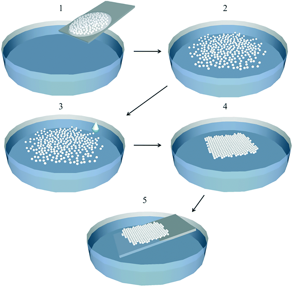
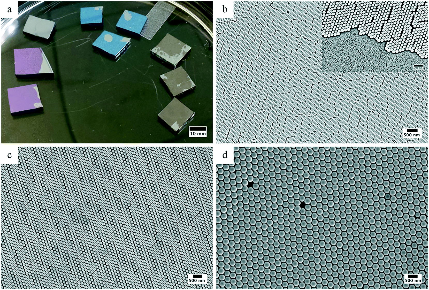
We fabricated large 2D HCP monolayer NS crystals using an indirect method via assembly at an air/liquid interface. This method is distinct from spin-coating and other techniques where the NS crystal is formed directly on a substrate.40,46,47 In this process, the NS crystal self-assembles into a floating monolayer on an intermediate liquid substrate and provides excellent mobility for production of larger defect-free areas and easy transfer to a substrate.46 We generated several different monolayers by using NS of different diameters (85 nm, 200 nm, and 400 nm polystyrene (PS) NS) in 2.5% w/v aqueous suspensions (Polysciences); the sizes of the NS were confirmed via SEM and the actual sizes of the NS that were used in this study are 85 nm, 190 nm, and 384 nm, respectively. Before the assembly at the air/liquid interface, the PS NS were centrifuged and resuspended in equal parts of water and ethanol at 5% w/v. A small volume of bead suspension (10–15 μl) was applied to a clean glass substrate and then was immersed at a shallow angle (20–30°) relative to the water surface into a 100 mm diameter glass dish filled with 20 ml 18.2 Ω cm de-ionized water (Fig. 1, step 1). The NS suspension spread across the water surface and formed a loosely ordered monolayer at the air/water interface (Fig. 1, step 2). We then applied a small volume (4–6 μl) of 2% w/v sodium dodecyl sulfate (SDS) to the liquid substrate, which forced the beads into a stable HCP crystalline monolayer (Fig. 1, steps 3 and 4). Assembly of the crystalline NS monolayer via the lateral SDS-induced capillary forces was demonstrated by a characteristic surface iridescence (Fig. 2a).47–49 We removed the NS monolayer from the liquid surface by essentially reversing the process of loading; we slowly immersed a clean substrate below the monolayer at a shallow angle (20–30°) and allowed the less dense (water/ethanol/bead) suspension to spread across the capture surface before withdrawing the capture surface containing the NS film (Fig. 1, step 5). As the NS monolayer dried, it underwent further ordering and packing. We used several different cleaned substrates: borosilicate glass coverslips, polystyrene (PS) Petri dishes (Fisher Scientific); silicon wafers <100> (Ted Pella); polyethylene terephthalate films (PepsiCo). The crystalline NS monolayer that was on the collecting substrates displayed an opalescence that is similar to that of the liquid born NS film prior to capture (Fig. 2b). The NS films on the substrates exhibited a size-dependent color under low-angle diffuse lighting; silicon chips that have been masked with three bead sizes (85 nm, 200 nm, and 400 nm) displayed characteristic colors based on bead size revealing gray, blue, and violet films, respectively (Fig. 3a). Scanning electron micrographs show high-quality packing of all three films (Fig. 3b–d). However, we observed some defects in the packing that appeared to be generated or exaggerated during imaging. We have selected two point defects or vacancies to highlight this type of defect while simultaneously showing that these are indeed monolayers (Fig. 3d). We observed other defects such as slip dislocations or line defects and polycrystalline domains. The larger variance in the smaller NS sizes that was observed in the 85 nm NS resulted in out-of-plane dislocation of larger-diameter beads from the monolayer (Fig. S1,† arrows). Another advantage of forming an NS monolayer at an air/liquid interface is the ability to apply the NS monolayer to non-planar surfaces and/or rough substrates (Fig. 4a–c). Previous work has demonstrated the application of a NS film onto macroscopic cylinders for the generation of 200 nm TiO2 nanopillar arrays;45 here, we demonstrated an even finer application of the technique by applying a NS mask to rough corners (Fig. 4b and c) and the masking of a 500 nm diameter irregular cylindrical structure (Fig. 4d).
 |
| | Fig. 1 Assembling and transferring a NS monolayer at the air/liquid interface. 1) Application of the bead suspension to a hydrophilic substrate; 2) generation of a floating disordered NS film; 3) application of SDS; 4) ordering of the NS monolayer on the liquid surface; 5) removal of the NS monolayer. | |
 |
| | Fig. 2 NS crystal monolayer assembly at the air/liquid interface and on a PS substrate. a) 400 nm NS monolayer film on the surface of a liquid covering ∼25 cm2. b) 400 nm NS monolayer transferred to the PS substrate. | |
 |
| | Fig. 3 Silicon wafer substrates masked with NS of different sizes. a) NS masks on silicon chips: left, 400 nm NS mask, violet hue; center, 200 nm NS mask, blue hue; right, 85 nm NS mask, gray hue; b–d) SEM micrographs of NS masks on a Si wafer: b) 85 nm NS mask; c) 200 nm NS mask; d) 400 nm NS mask. | |
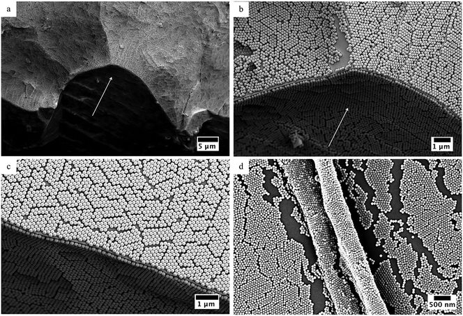 |
| | Fig. 4 SEM micrographs of NS masking non-planar surfaces. a) 200 nm NS film conforming to a silicon wafer fragment with an irregular surface. b) Higher magnification of the region in (a). c) ∼90° edge with a 200 nm NS monolayer showing acceptance of the film with packing. d) 500 nm cylinder with an 85 nm NS mask exhibiting HCP organization. | |
SEM imaging.
Scanning electron micrographs were obtained using a Zeiss Auriga SEM with an accelerating voltage of 2–4 kV (30 μm or 7.5 μm aperture) and an in-lens SESI detector. Samples were glow coated with a 5 nm gold layer using a Leica EM ACE200 that is equipped with a real-time thickness monitoring system using a quartz crystal microbalance. Image processing and analysis including the measurement of the nanoscale features of the NSS was performed using ImageJ software. Illustrations were made using Google Sketchup. To calculate the dimensions of the NSS using the SEM images, we used simple trigonometric calculations for the surface areas of cylindrical and conical shapes (Fig. S2†). Face-on view at 0° stage tilt allows us to determine the unit cell measurements, base diameter, and pitch/center-to-center spacing (Fig. S2a†). All measurements were collected from at least 10 independent nanoscale features from at least three separate samples from high-magnification SEM images taken at 45° tilt (Fig. S2b–d†). The roughness factor (Rf) was determined as the ratio of the total surface area to the projected flat area.50,51
Plasma etching and reactive ion etching.
We etched the NS-masked substrates using South Bay Technology Model PC-2000 plasma cleaners with oxygen as the process gas. For isotropic plasma etching (PE), we mounted the polymeric substrates on the grounded base of the plasma chamber and plasma-treated them at 100 W forward power and 200 mT chamber pressure for defined exposure times that were dependent on the NS diameter and targeted nanostructure geometry. Mounting the masked substrates directly on a self-biased RF-powered electrode allowed anisotropic reactive ion etching (RIE); for all REI NSS, we used the same process parameters: 100 W forward power, −700 V DC bias, and 200 mT chamber pressure. Etch rates were determined using ImageJ analysis of high-resolution/scaled scanning electron micrographs of NS films on silicon wafers that had been PE. Masked substrates were PE performed using oxygen plasma with the following parameters: 50 W forward power at ∼200 mT. The samples were etched for definite times: 20 minutes for 200 nm NS and 16 minutes for 400 nm NS (Fig. 5a and d). 8-bit grey-scale images were manually thresholded and then converted to binary images (Fig. 5b and c). The fit ellipse function was used with a 0.9 circularity constraint to determine the NS diameter using the average axis value. We excluded particles that did not meet the constraints, as charging during imaging resulted in eccentricities in the binary image (Fig. 5e and f arrows). Reactive ion etching provides a linear relationship for axial diameter reduction but a nonlinear transverse relationship (Fig. S3†). Inspection of the best-fit equations yields etch rates (slopes) that are in agreement across bead diameters, which is useful for extrapolation to other NS diameters eliminating the need to map them out (Fig. 4 and 5). The resulting PE treatment that altered the NS size also altered the optical properties of these NS film-containing surfaces as described in Fig. 3a (Fig. S4c†). Superimposing plots and looking at horizontal intercepts and/or using the fit equations allow us to target common mask particle sizes across the various pitches as defined by the initial bead diameter (Fig. S5†).
 |
| | Fig. 5 Process flow for measuring NS size and determining etch rate parameters. Nanostructures were measured using ImageJ. SEM images of a) 200 nm nanospheres, 20 min exposure time and d) 400 nm nanospheres, 16 min exposure time. Binary images of manually thresholded SEM images above b) 200 nm NS and e) 400 nm NS. Fitted ellipses of the binary images above while discriminating for size and circularity to sharpen data by removing artifacts: c) 200 nm NS and f) 400 nm NS. | |
Static contact angle/wettability.
We collected static contact angle (CA) measurements using a ramé-hart 260-F4 contact angle goniometer and DROPimage Advanced software. We measured the angle of a 1 μl drop of deionized 18.2 MΩ cm water on gold-coated and non-coated substrates. CA measurements were made on at least five drops on three different samples of each surface; data was analyzed using the Student's t-test function in Microsoft Excel.
Results and discussion
Plasma-etched PET NSS
The HCP pattern displayed by the NS monolayers mimics the distribution of the conical structures found on the wings of many cicada species, including the dog day cicada Tibicens spp.10,12,15,38,52 The isotropic PE of a 400 nm NS-masked polyethylene terephthalate (PET) substrate resulted in unique hierarchical pyramidal NSS (Fig. 6). The nanoscale features generated by the PE are nanoscale concave hexagonal pyramid structures that resemble circus tents or inverted umbrellas (Fig. 6c, inset). Each of the three concave faces of the tetrahedral interstices resulting from the HCP NS arrangement inversely reflects one of the concave triangular faces on three adjacent structures. Each pyramid is framed by six 10–20 nm wide nanoscale buttresses that extend from the tip to the base and these buttress ridges correspond to contacting radii of adjacent spheres (Table 1). Incomplete etching results in a remnant of the NS mask on the apex of the nanopyramid (Fig. 6a, arrow). Longer etch times resulted in thinner, wiry tips. We removed the remnants of the NS mask via sonication. While short post-etching sonication does not damage the shallow pyramidal structures of this NSS, inadequate sonication results in contamination of the surface with the deposition of the remnants of the NS mask in the areas between nanopyramids (Fig. 6b, arrow); optimized sonication/successful cleaning results in the removal of all masking remnants (Fig. 6c and inset). Longer sonication, however, damages the surface significantly (Fig. S6a and b†).
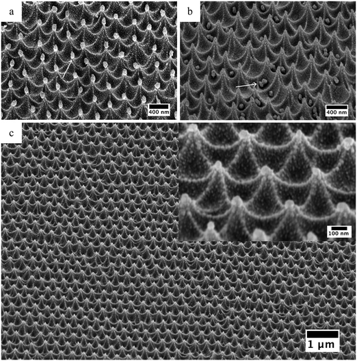 |
| | Fig. 6 SEM micrographs of isotropic plasma-etched PET NSS. a) SEM image of 10 min etched NSS (100 W, 200 mT); b) isotropic PET NSS after incomplete sonication, note the remnant of a NS in the depression between the spires (arrow); c) isotropic PET NSS after complete sonication, inset: nanopyramid tips are devoid of NS remnants. | |
Table 1 Summary of physical characteristics of polymeric NSS
| Surface |
Nanofeature shape |
Center-to-center spacing (nm) |
Base diameter (nm) |
Tip diameter (nm) |
Height (nm) |
Roughness factor (Rf) |
| Dog day cicada (Tibicens spp.), Fig. 7a |
Conical |
167 ± 23 |
125 ± 12 |
67 ± 23 |
286 ± 17 |
— |
| PET isotropically PE with 200 nm NS mask, 10 minute etch, Fig. 6c |
Pyramidal |
376 ± 25 |
376 ± 25 |
<50 nm |
383 ± 15 |
— |
| PET anisotropically RIE with 400 nm NS mask, 90 second etch, Fig. 8f |
Conical |
360 ± 16 |
350 ± 22 |
62 ± 8 |
630 ± 32 |
3.4 ± 0.43 |
| PET anisotropically etched with 200 nm NS mask, 45 second etch, Fig. 7c |
Thin conical |
172 ± 20 |
151 ± 13 |
49 ± 6 |
268 ± 31 |
2.9 ± 0.79 |
| PET anisotropically etched with 200 nm NS mask, 30 second etch, Fig. 7b |
Stout conical/capped |
178 ± 20 |
104 ± 5 |
84 ± 4 |
208 ± 11 |
— |
| PS anisotropically RIE with 400 nm NS mask, 90 second etch, Fig. 9d |
Conical |
372 ± 22 |
234 ± 8 |
81 ± 8 |
388 ± 32 |
1.9 ± 0.28 |
| PS anisotropically etched with 200 nm NS mask, 45 second etch, Fig. 9f |
Conical |
171 ± 10 |
108 ± 3 |
40 ± 2 |
167 ± 8 |
1.8 ± 0.24 |
| PS anisotropically etched with 85 nm NS mask, 15 second etch, Fig. 9g |
Hemispherical |
72 ± 7 |
40 ± 5 |
33 ± 5 |
13 ± 2.8 |
3.7 ± 0.97 |
Anisotropic RIE of NS-masked PET and PS substrates
Isotropic RIE of a PET substrate that had been masked with 200 nm polystyrene NS resulted in a conical nanostructure geometry (Fig. 7b) that mimicked the NSS found on the wings of the dog day cicada (Fig. 7a; Table 1). This is the first demonstration of the use of the NSL technique for biomimetic replication of a known natural NSS in a synthetic polymer. One of the intriguing aspects of the NSL technique is its ability to fabricate NSS that are structurally distinct from native NSS simply by changing one parameter of the process. For instance, by increasing the time of etching of the same masked substrate that generated the biomimetic NSS, we produced a different NSS with nanoscale features that had a higher aspect ratio than those found on the dog day cicada wing (Fig. 7c; Table 1).
 |
| | Fig. 7 SEM images of biomimetic PET NSS and dog day cicada wings. a) Native NSS from a dog day cicada wing (Tibicens spp.); b) PET NSS generated by a 200 nm NS mask fabricated with a 30 second RIE; c) PET NSS fabricated with a 45 second RIE. | |
Another way to generate synthetic polymeric NSS that are structurally distinct from natural NSS using the NSL technique is to use NS of different sizes in the masking process. We fabricated a NSS using a 400 nm NS mask on a PET substrate and, as expected, the resulting surface exhibited an HCP array of nanocones that were double the scale of features in our synthetic biomimetic arrays with a larger center-to-center distance (Table 1). Increasing the time of RIE increased the aspect ratio of the features (compare Fig. 8d and f) and increased the area between the features (Fig. 8cvs. e), but did not change the center-to-center spacing of the nanoscale features, which is a function of the size of the NS used as the mask (Table 1). Truncated etches (60 seconds) of the 400 nm NS-masked PET substrates do not completely remove the PS NS mask and result in shorter and thicker composite PS/PET features (Fig. 8d, arrow), which may be useful for the generation of hybrid 2D materials.
 |
| | Fig. 8 PET NSS generated via masking with 400 nm NS and RIE. (a–d) Etch time, 60 seconds; (e and f) etch time, 90 seconds. a and b) 45° tilt, lower magnification demonstrating the uniformity of the NSS array; c) face-on/0° tilt image, note the ridges traversing the interstices, arrow; d) 45° tilt high magnification clearly showing capping and striations; the NS remnants on top of each nanoscale cone, arrow; e) face-on/0° tilt image, longer etch times result in smaller conical cross-sections, larger areas between the cones, and longer ridges connecting the cones. f) Longer etching result in nanoscale features with higher aspect ratios and smaller NS remnant caps (arrow). | |
In addition to the conical nanoscale features, PET nanostructures that were generated by RIE exhibited a hierarchical pattern. Each nanocone in the NSS displayed 10–20 nm wide axial striations along the length of each cone (Fig. 8d and f); these nanoscale striations extended onto the area between the nanofeatures (Fig. 8c-arrow and e). Similar axial nanoscale striations along the lengths of nanocones have been reported in NSS generated in PMMA via the NSL process,41 which suggests that the polymer structure may play a role in the formation of hierarchical NSS.
We generated NSS in another synthetic polymer PS, which allowed us to determine whether other polymeric substrates processed by the NSL technique generated NSS with hierarchical nanoscale features. PS was etched more rapidly than PET and generated NSS with conical features that were smaller than the features from comparable PET NSS (Table 1). Partial etching (45 s RIE) of a PS substrate masked with 400 NS resulted in stocky short columns with large NS remnants (Fig. 9a and b). Longer etching of the same surface resulted in complete etching of the surface with the removal of the NS mask and thinner, higher-aspect ratio nanoscale features (Fig. 9d and e; Table 1). The resultant NSS also displayed an angle-dependent structural color (Fig. 9c). Although this structural optical effect is similar to other 2D diffraction gratings/photonic crystals,53,54 this material is unique in that it is a NSS photonic crystal that is composed of a synthetic polymer; furthermore, the PS NSS materials are flexible, and may have applications in sensing or photonics.55 The PS nanoscale features that were fabricated by NSL were also qualitatively different from those generated in PET. PS nanocones were smoother than PET nanocones and displayed a grid of 20–40 nm tall ridges in the interstitial area between the nanocones conjoining the bases (Fig. 9d, arrow). This result suggests that the polymer substrate in part determines the hierarchical nanoscale features during NSL and that by selecting different polymers the hierarchical structure of a synthetic NSS may be controlled.
 |
| | Fig. 9 Synthetic PS NSS fabricated via NSL. (a–e) PS nanocones fabricated with a 400 nm NS mask. a and b) 45 second RIE showing the intermediate stage of nanocone formation with partially etched NS atop the cylindrical nanofeatures (b, arrow); c) angle-dependent scattering of light of the PS NSS shown in (d) from violet/highest viewing angle to red/lowest viewing angle; d) PS NSS generated by a 90 second RIE showing discrete cones with defined grid-patterned ridges between cones (arrow); e) 2 minute RIE of a 400 NS-masked PS substrate resulted in higher-aspect ratio PS nanocones; f) PS NSS generated from a 200 nm NS mask and 45 s RIE. g) PS NSS fabricated using an 85 nm NS mask and 15 second RIE, (inset) note the hemispherical nanoscale features. | |
As demonstrated in the fabrication of PET NSS, by using different sized masking NS, we altered the size, distribution, and scale of the nanostructures within an NSS. PS NSS fabricated with a 200 nm NS mask displayed discrete conical nanoscale features that were similar to those made in PET NSS, although again the features themselves were smaller and smoother (Fig. 9f, inset; Table 1). Interestingly, when we NSL-processed PS that was masked with the 85 nm NS, we lost the conical geometry and produced instead an array of small 40 nm hemispherical capped columns (Fig. 9g, inset; Table 1).
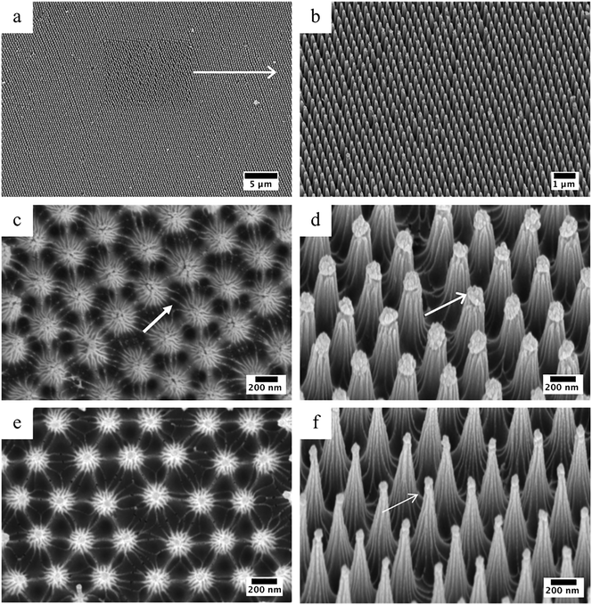
Directed synthesis of hierarchical NSS
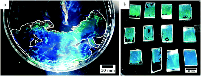
The polymeric NSS that were fabricated by NSL here and by others had hierarchical nanoscale features that resulted from ion/polymer interactions during the etching process.41 Although these types of hierarchical NSS have enormous potential due to the diversity of polymers and potential etchants, control over these features may be limited. We imagined that we could generate other hierarchical NSS by manipulating the NSL process itself. Although the use of a double NS layer mask prior to RIE has been used to generate NSS that exhibit unique surface topographies in silicon,40 these surfaces do not exhibit a hierarchical structure. In this paper, we demonstrated that NSL permits the directed fabrication of a hierarchical, multiplexed NSS by reiterating the masking process sequentially on a single substrate. In this proof-of-concept demonstration, we sequentially masked a PS substrate with two different sizes of NS: mask 1 – 400 nm NS and mask 2 – 85 nm NS (Fig. 10). In the first round of NSL, we fabricated a conical PS NSS with a 400 nm bead mask after 90 seconds of RIE (Fig. 10, 11b and c); this surface would then serve as the substrate for the next step. In the second round of NSL, we masked the 400 nm conical NSS substrate with 85 nm NS and processed this surface using a 30 second RIE (Fig. 10, 11a, c and e). Interestingly, the NS mask altered the spectral properties of the original 400 nm NSS which appears blue, while the hybrid 85 nm PS NS-masked 400 nm NSS appears green (Fig. 11a inset). The directed hierarchical NSS exhibits three levels of hierarchy – two distinct nanoscale conical features and the axial striations on the larger cones (Fig. 11b, d and f). While nanoscale hierarchical surfaces have been made previously, a hierarchical ZnO nanomaterial has recently been fabricated using interference lithography;56 the directed multistep NSL approach that we describe will facilitate the fabrication of a broader variety of types of hierarchical NSS in a wider range of materials.
 |
| | Fig. 10 Schematic of multi-step NSL for the fabrication of directed hierarchical NSS. | |
 |
| | Fig. 11 SEM micrographs of directed hierarchical NSS via reiterative NSL. a, c and e) Images after the second mask showing a 400 nm NS mask-generated PS NSS substrate with an 85 nm PS NS mask. Inset of (a) demonstrates the shift in the opalescence from blue color of larger cones (left, arrow) to green when overlaid with an 85 nm diameter NS film; b, d and f) SEM images of the hierarchical NSS after a 30 second RIE following the second 85 nm NS mask. b) The overall order of the NSS remains intact showing a uniform HCP structure; d) smaller nanofeatures are clearly observed between the larger nanocones (arrow); f) these smaller nanocones occupy all of the interstitial area (arrow); the original cones are thinner after second etching (thicker cone). | |
Polymeric synthetic NSS wettability
Both native and synthetic NSS have been shown to have altered wettability.29,41,57 To demonstrate that nanoscale structuring PS and PET substrates also affected the wettability, we determined the static contact angle on uncoated NSS and NSS coated with 2 nm of Au. The addition of a thin layer of Au has been shown to mask underlying surface compositional effects and permit the comparison between compositionally similar but structurally different materials.38 Both control flat PS and PET substrates exhibit modest wettability as demonstrated by their static contact angle: flat uncoated PS – CA = 85°; flat Au-coated PS – CA = 78°; flat uncoated PET – CA = 74°; flat Au-coated PET – CA = 96° (Fig. 12a and c). However, synthetic NSS that were generated with REI processing of the 200 nm NS-masked PS substrate resulted in a superhydrophilic surface (Fig. 12b, left upper inset, CA < 10°). If this same surface is coated with a 2 nm layer of gold, the surface becomes hydrophobic (Fig. 12b, right upper inset, CA = 102°). This trend was true for all PET NSS as well, except for the PET nanopyramid array that was fabricated by PE (Fig. 12e); all of the PET NSS exhibited a similar shift in wettability from hydrophilic to hydrophobic (Fig. 12d and f–h). The tunable nature of the wettability of these polymeric NSS generated by NSL by the simple addition of a nanoscale layer to the surface suggests that they may serve as important tools for water salvaging from the atmosphere or the wicking of water in specific areas.41,56
 |
| | Fig. 12 Static contact angles of PET and PS NSS. Insets of all images: upper left hand inset, uncoated surface CA images of a 1 μl dH2O water drop; upper right hand inset, CA image of a 1 μl dH2O water drop on a surface coated with a 2 nm layer of gold. a and b) PS surfaces: a) flat PS control substrate; b) PS NSS generated by anisotropic 90 second RIE of a 400 nm NS-masked flat polystyrene substrate. c–h) PET substrates: c) flat control PET substrate; d) PET NSS generated by anisotropic 60 second RIE of a 400 nm NS-masked flat PET substrate; e) PET NSS generated by isotropic 10 minute PE of a 400 nm NS-masked flat PET substrate; f) PET NSS generated by anisotropic 45 second RIE of a 200 nm NS-masked flat PET substrate; g) PET NSS generated by anisotropic 60 second RIE of a 400 nm NS-masked flat PET substrate; h) PET NSS generated by anisotropic 30 second RIE of a 200 nm NS-masked flat PET substrate. | |
Conclusions
NSL is a powerful and versatile technique that enables the fabrication of NSS which have an enormous diversity in nanoscale feature shape, size, distribution, and hierarchical complexity. We have also shown that the polymeric NSS generated by this method have interesting and useful optical and physical properties that are tunable and have potential applications in a range of areas including antimicrobial surface treatments, solar energy, and optics. Furthermore, the combination of single- or multi-step NSL processes with other bottom-up and/or top-down fabrication processes will enable the generation/reproduction of other biomimetic NSS and the creation of completely novel bio-inspired materials.
Author contributions
Dr. Kyle Nowlin performed the experiments in this paper as well as collected the data and assisted in the experimental design as part of his doctoral dissertation; Dr. Dennis LaJeunesse assisted in the experimental design and data analysis and the writing of this manuscript.
Funding sources
North Carolina Biotechnology Center (NCBC) Biotechnology Research Grant (213-BRG-1209 to Dr. Dennis LaJeunesse).
Abbreviations
| PET | Polyethylene terephthalate |
| NSS | Nanostructured surface |
| PS | Polystyrene |
| PE | Plasma etching |
| RIE | Reactive ion etching |
| SDS | Sodium dodecyl sulfate |
| HCP | Hexagonal close packed |
| NSL | Nanosphere lithography |
| NS | Nanosphere/nanospheres |
Acknowledgements
This work was supported by a North Carolina Biotechnology Center (NCBC) Biotechnology Research Grant (213-BRG-1209 to Dr. Dennis LaJeunesse) and through generous assistance of Dr. James Ryan, the Joint School of Nanoscience and Nanoengineering, and the State of North Carolina.
References
- N. M. Teets,
et al., Gene expression changes governing extreme dehydration tolerance in an Antarctic insect, Proc. Natl. Acad. Sci. U. S. A., 2012, 109(50), 20744–20749 CrossRef CAS PubMed.
- T. M. Clark, B. J. Flis and S. K. Remold, pH tolerances and regulatory abilities of freshwater and euryhaline Aedine mosquito larvae, J. Exp. Biol., 2004, 207(13), 2297–2304 CrossRef PubMed.
- M. S. Clark,
et al., Surviving the cold: molecular analyses of insect cryoprotective dehydration in the Arctic springtail Megaphorura arctica (Tullberg), BMC Genomics, 2009, 10, 328 CrossRef PubMed.
- A. Skordos,
et al., A novel strain sensor based on the campaniform sensillum of insects, Philos. Trans. R. Soc., A, 2002, 360(1791), 239–253 CrossRef CAS PubMed.
- F. De Nicola,
et al., Moth-eye effect in hierarchical carbon nanotube anti-reflective coatings, Carbon, 2016, 108, 262–267 CrossRef CAS.
- S. C. Park,
et al., Fabrication and characterization of moth-eye mimicking nanostructured convex lens, Microelectron. Eng., 2016, 158, 35–40 CrossRef CAS.
- F. Galeotti,
et al., Broadband and crack-free antireflection coatings by self-assembled moth eye patterns, ACS Appl. Mater. Interfaces, 2014, 6(8), 5827–5834 CAS.
- J. A. Watson,
et al., A Dual Layer Hair Array of the Brown Lacewing: Repelling Water at Different Length Scales, Biophys. J., 2011, 100(4), 1149–1155 CrossRef CAS PubMed.
- G. S. Watson, B. W. Cribb and J. A. Watson, Contrasting micro/nano architecture on termite wings: two divergent strategies for optimising success of colonisation flights, PLoS One, 2011, 6(9), e24368 CAS.
- M. Sun,
et al., A study of the anti-reflection efficiency of natural nano-arrays of varying sizes, Bioinspiration Biomimetics, 2011, 6(2), 026003 CrossRef PubMed.
- H. M. S. Hu,
et al., Non-wetting wings and legs of the cranefly aided by fine structures of the cuticle, J. Exp. Biol., 2011, 214(6), 915–920 CrossRef PubMed.
- M. Sun,
et al., Wetting properties on nanostructured surfaces of cicada wings, J. Exp. Biol., 2009, 212(19), 3148–3155 CrossRef PubMed.
- G. S. Watson,
et al., Putative functions and functional efficiency of ordered cuticular nanoarrays on insect wings, Biophys. J., 2008, 94(8), 3352–3360 CrossRef CAS PubMed.
- A. Boseman,
et al., Ultrastructural analysis of wild type and mutant Drosophila melanogaster using helium ion microscopy, Micron, 2013, 51, 26–35 CrossRef CAS PubMed.
- R. Chandran,
et al., SEM characterization of anatomical variation in chitin organization in insect and arthropod cuticles, Micron, 2016, 82, 74–85 CrossRef CAS PubMed.
- S. N. Gorb,
et al., Insects did it first: a micropatterned adhesive tape for robotic applications, Bioinspiration Biomimetics, 2007, 2(4), S117–S125 CrossRef PubMed.
- N. Hosoda and S. N. Gorb, Underwater locomotion in a terrestrial beetle: combination of surface de-wetting and capillary forces, Proc. R. Soc. B, 2012, 279(1745), 4236–4242 CrossRef PubMed.
- A. E. Kovalev, A. E. Filippov and S. N. Gorb, Insect wet steps: loss of fluid from insect feet adhering to a substrate, J. R. Soc., Interface, 2013, 10(78), 20120639 CrossRef PubMed.
- K. Kuitunen and S. N. Gorb, Effects of cuticle structure and crystalline wax coverage on the coloration in young and old males of Calopteryx splendens and Calopteryx virgo, Zoology, 2011, 114(3), 129–139 CrossRef PubMed.
- K. Kuitunen, A. Kovalev and S. N. Gorb, Sex-related effects in the superhydrophobic properties of damselfly wings in young and old calopteryx splendens, PLoS One, 2014, 9(2), e88627 Search PubMed.
- S. Yoshioka,
et al., Coloration using higher order optical interference in the wing pattern of the Madagascan sunset moth, J. R. Soc., Interface, 2008, 5(21), 457–464 CrossRef CAS PubMed.
- M. Kolle,
et al., Mimicking the colourful wing scale structure of the Papilio blumei butterfly, Nat. Nanotechnol., 2010, 5(7), 511–515 CrossRef CAS PubMed.
- A. R. Parker, 515 million years of structural colour, J. Opt. A: Pure Appl. Opt., 2000, 2(6), R15–R28 CrossRef.
- J. Sun, B. Bhushan and J. Tong, Structural coloration in nature, RSC Adv., 2013, 3(35), 14862–14889 RSC.
- P. Simonis and J. P. Vigneron, Structural color produced by a three-dimensional photonic polycrystal in
the scales of a longhorn beetle: Pseudomyagrus waterhousei (Coleoptera: Cerambicidae), Phys. Rev. E: Stat., Nonlinear, Soft Matter Phys., 2011, 83(1 Pt 1), 011908 CrossRef PubMed.
- E. Shevtsova,
et al., Stable structural color patterns displayed on transparent insect wings, Proc. Natl. Acad. Sci. U. S. A., 2011, 108(2), 668–673 CrossRef CAS PubMed.
- Y. Fu,
et al., Structural colors: from natural to artificial systems, Wiley Interdiscip. Rev.: Nanomed. Nanobiotechnol., 2016, 8(5), 758–775 CrossRef PubMed.
- K. C. Park,
et al., Nanotextured Silica Surfaces with Robust Superhydrophobicity and Omnidirectional Broadband Supertransmissivity, ACS Nano, 2012, 6(5), 3789–3799 CrossRef CAS PubMed.
- K. M. Wisdom,
et al., Self-cleaning of superhydrophobic surfaces by self-propelled jumping condensate, Proc. Natl. Acad. Sci. U. S. A., 2013, 110(20), 7992–7997 CrossRef CAS PubMed.
- G. S. Watson, B. W. Cribb and J. A. Watson, How micro/nanoarchitecture facilitates anti-wetting: an elegant hierarchical design on the termite wing, ACS Nano, 2010, 4(1), 129–136 CrossRef CAS PubMed.
- X. Ye,
et al., Microstructure of superhydrophobic surfaces from natural to artificial, Nami Jishu Yu Jingmi Gongcheng, 2009, 7(5), 381–386 Search PubMed.
-
G. Sun and Y. Fang, Special wettability of locust wing and preparation of biomimetic polymer film by soft lithography, in Advances in Energy, Environment and Materials Science – Proceedings of the International Conference on Energy, Environment and Materials Science, EEMS 2015, 2016 Search PubMed.
- Y. F. Huang,
et al., Design for approaching cicada-wing reflectance in low- and high-index biomimetic nanostructures, ACS Nano, 2015, 9(1), 301–311 CrossRef CAS PubMed.
- M. N. Dickson,
et al., Nanopatterned polymer surfaces with bactericidal properties, Biointerphases, 2015, 10(2), 021010 CrossRef PubMed.
- Y. Kanamori,
et al., 100 nm period silicon antireflection structures fabricated using a porous alumina membrane mask, Appl. Phys. Lett., 2001, 78(2), 142–143 CrossRef CAS.
- Y. Lee, Fabrication of hierarchical structures on a polymer surface to mimic natural superhydrophobic surfaces, Adv. Mater., 2007, 19(17), 2330–2335 CrossRef CAS.
- H. Li,
et al., Simulation of the electrohydrodynamic instability process used in the fabrication of hierarchic and hollow micro/nanostructures, RSC Adv., 2014, 4(27), 13774–13781 RSC.
- K. Nowlin,
et al., Adhesion-dependent rupturing of Saccharomyces cerevisiae on biological antimicrobial nanostructured surfaces, J. R. Soc., Interface, 2015, 12(102), 20140999 CrossRef.
- W. Li,
et al., Fabrication of large-scale periodic silicon nanopillar arrays for 2D nanomold using modified nanosphere lithography, Appl. Surf. Sci., 2007, 253(22), 9035–9038 CrossRef CAS.
- C. L. Cheung,
et al., Fabrication of nanopillars by nanosphere lithography, Nanotechnology, 2006, 17(5), 1339–1343 CrossRef CAS.
- D. Wang,
et al., Bioinspired ribbed hair arrays with robust superhydrophobicity fabricated by micro/nanosphere lithography and plasma etching, RSC Adv., 2015, 5(117), 96404–96411 RSC.
- C. R. Henry, 2D-Arrays of Nanoparticles as Model Catalysts, Catal. Lett., 2015, 145(3), 731–749 CrossRef CAS.
- P. Colson, C. Henrist and R. Cloots, Nanosphere lithography: A powerful method for the controlled manufacturing of nanomaterials, J. Nanomater., 2013, 2013, 948510 Search PubMed.
- F. J. Wendisch,
et al., Confined etching within 2D and 3D colloidal crystals for tunable nanostructured templates: Local environment matters, ACS Appl. Mater. Interfaces, 2017, 9(4), 3931–3939 CAS.
- L. Berthod,
et al., Colloidal photolithography applied to functional microstructure on cylinder based on photopatternable TiO2 sol-gel, Microelectron. Eng., 2017, 177, 46–51 CrossRef CAS.
- Y. Zhang,
et al., Ordered nanostructures array fabricated by nanosphere lithography, J. Alloys Compd., 2008, 452(2), 473–477 CrossRef CAS.
- P. A. Kralchevsky and K. Nagayama, Capillary forces between colloidal particles, Langmuir, 1994, 10(1), 23–36 CrossRef CAS.
- J. Rybczynski, U. Ebels and M. Giersig, Large-scale, 2D arrays of magnetic nanoparticles, Colloids Surf., A, 2003, 219(1–3), 1–6 CrossRef CAS.
-
K. Nojiri, Dry etching technology for semiconductors, Dry Etching Technology for Semiconductors, 2015, pp. 1–116 Search PubMed.
- E. S. Gadelmawla,
et al., Roughness parameters, J. Mater. Process. Technol., 2002, 123(1), 133–145 CrossRef.
- L. C. Hsu,
et al., Effect of micro- and nanoscale topography on the adhesion of bacterial cells to solid surfaces, Appl. Environ. Microbiol., 2013, 79(8), 2703–2712 CrossRef CAS PubMed.
- G. S. Watson,
et al., Putative functions and functional efficiency of ordered cuticular nanoarrays on insect wings, Biophys. J., 2008, 94(8), 3352–3360 CrossRef CAS PubMed.
- Y. Liu,
et al., Bio-inspired micro-nano structured surface with structural color and anisotropic wettability on Cu substrate, Appl. Surf. Sci., 2016, 379, 230–237 CrossRef CAS.
- L. Petti,
et al., Fabrication of novel two-dimensional nanopatterned conductive PEDOT:PSS films for organic optoelectronic applications, ACS Appl. Mater. Interfaces, 2013, 5(11), 4777–4782 CAS.
- Y. Yue and J. P. Gong, Tunable one-dimensional photonic crystals from soft materials, J. Photochem. Photobiol., C, 2015, 23, 45–67 CrossRef CAS.
- Z. Wang,
et al., Wicking Enhancement in Three-Dimensional Hierarchical Nanostructures, Langmuir, 2016, 32(32), 8029–8033 CrossRef CAS PubMed.
- Y. Y. Yan, N. Gao and W. Barthlott, Mimicking natural superhydrophobic surfaces and grasping the wetting process: A review on recent progress in preparing superhydrophobic surfaces, Adv. Colloid Interface Sci., 2011, 169(2), 80–105 CrossRef CAS PubMed.
Footnote |
| † Electronic supplementary information (ESI) available. See DOI: 10.1039/c7me00009j |
|
| This journal is © The Royal Society of Chemistry 2017 |
Click here to see how this site uses Cookies. View our privacy policy here. 
 *
*