
Subnanometer structure and function from ion beams through complex fluidics to fluorescent particles†
Kuo-Tang
Liao
 ab,
Joshua
Schumacher
a,
Henri J.
Lezec
a and
Samuel M.
Stavis
*a
ab,
Joshua
Schumacher
a,
Henri J.
Lezec
a and
Samuel M.
Stavis
*a
aCenter for Nanoscale Science and Technology, National Institute of Standards and Technology, Gaithersburg, Maryland 20899, USA. E-mail: samuel.stavis@nist.gov
bMaryland Nanocenter, University of Maryland, College Park, Maryland 20742, USA
First published on 29th November 2017
Abstract
The vertical dimensions of complex nanostructures determine the functions of diverse nanotechnologies. In this paper, we investigate the unknown limits of such structure–function relationships at subnanometer scales. We begin with a quantitative evaluation of measurement uncertainty from atomic force microscopy, which propagates through our investigation from ion beam fabrication to fluorescent particle characterization. We use a focused beam of gallium ions to subtractively pattern silicon surfaces, and silicon nitride and silicon dioxide films. Our study of material responses quantifies the atomic limits of forming complex topographies with subnanometer resolution of vertical features over a wide range of vertical and lateral dimensions. Our results demonstrate the underutilized capability of this standard system for rapid prototyping of subnanometer structures in hard materials. We directly apply this unprecedented dimensional control to fabricate nanofluidic devices for the analytical separation of colloidal nanoparticles by size exclusion. Optical microscopy of single nanoparticles within such reference materials establishes a subnanometer limit of the fluidic manipulation of particulate matter and enables critical-dimension particle tracking with subnanometer accuracy. After calibrating for optical interference within our multifunctional devices, which also enables device metrology and integrated spectroscopy, we reveal an unexpected relationship between nanoparticle size and emission intensity for common fluorescent probes. Emission intensity increases supervolumetrically with nanoparticle diameter and then decreases as nanoparticles with different diameters photobleach to similar values of terminal intensity. We propose a simple model to empirically interpret these surprising results. Our investigation enables new control and study of structure–function relationships at subnanometer scales.
Introduction
Structure determines function in nanotechnologies of all dimensionalities, including those with nanoscale vertical dimensions and similar or larger lateral dimensions. Control of the vertical dimensions of such nanostructures enables the fabrication of functional devices in diverse domains of nanotechnology. In this paper, we dramatically advance both the structural and functional aspects of this fundamental relationship, and we couple them so closely as to essentially integrate the subnanometer structure and function of complex devices. First, we investigate the unknown limits of controlling the vertical dimensions of silicius materials at atomic scales with a focused beam of gallium ions, quantifying subnanometer resolution over a wide range of vertical and lateral dimensions. Then, we apply this unprecedented control, fabricating nanofluidic devices that enable dimensional and optical metrology of single nanoparticles in liquids with record accuracy and precision.Since Feynman envisioned the focused ion beam as a foundation of nanotechnology,1 it has become extremely useful due to its unique capability to directly pattern hard materials with nanoscale resolution in three dimensions.2–7 This capability obviates lithographic pattern transfer and facilitates rapid prototyping of functional nanostructures. While many studies have used a focused ion beam to precisely control the lateral dimensions of nanostructures,2,8 few have precisely controlled their vertical dimensions,9–13 and none have quantified the related limits of dimensional control or demonstrated devices functioning near these limits. To do so requires a comprehensive investigation that integrates nanoscale fabrication, characterization, and application, as we report here. We study the unknown limits of the subtractive processing of silicon, silicon nitride, and silicon dioxide by a focused beam of gallium ions, investigating the different responses of these diverse materials at atomic scales. In the context of fabricating devices for practical applications, we identify design rules for rapid prototyping of complex patterns with subnanometer resolution of vertical dimensions over a wide range of vertical and lateral dimensions. Remarkably, using this standard system, some aspects of our vertical dimensional control extend below 0.1 nm. In this way, our investigation enables new control and study of structure–function relationships at subnanometer scales.
We demonstrate an application that requires and motivates this dimensional control. We fabricate nanofluidic devices for the analytical separation of nanoparticles by size exclusion, and track nanoparticles by optical microscopy within such reference materials to measure their size distribution. In this way, we establish a subnanometer limit of the fluidic manipulation of particulate matter, and enable critical-dimension particle tracking with subnanometer accuracy. In comparison to other fluidic methods of manipulating and measuring nanoparticles,14–18 which generally involve tracking particle motion or sensing device occlusion, our method is more direct and capable of resolving smaller nanoparticles. Moreover, our method is optimal for quantitative measurement of the optical properties of nanoparticles, which are among their most important properties and depend on their dimensions. Our measurements reveal an unexpected nonvolumetric relationship between the size and emission intensity of nanoparticles which commonly serve as fluorescent probes.19 These results are highly relevant to the many users of such nanoparticles in biological and other applications,20 and establish a firm foundation for future applications of our method such as in quality control of nanoparticle manufacturing. Further, in this measurement, we calibrate for optical interference effects within our complex devices, enabling future measurements of device dimensions by optical microscopy and on-chip integration of spectroscopic optics.
Results and discussion
Uncertainty evaluation
Considering our goal of quantifying the limits of subnanometer structure and function, a rigorous evaluation of measurement uncertainty is a prerequisite. We measure the vertical dimensions of surface features with an atomic force microscope, which we calibrate with a submicrometer reference material with a step depth of 183.6 nm ± 0.9 nm that is NIST traceable.21,22 We report all uncertainties as a confidence interval of 95% or we note otherwise. A quartic polynomial linearizes the sensor response with negligible error, resulting in a systematic uncertainty of 0.5% for all depths. We test this submicrometer calibration at subnanometer scales by measuring highly ordered pyrolytic graphite as an atomic reference material with a monolayer thickness of 0.335 nm, adding negligible absolute uncertainty of 0.006 nm, as Fig. S1† shows. We identify two other sources of measurement uncertainty that are significant. First, we quantify the variation in roughness of milled silicon (100) from different measurement parameters, as Fig. S2† shows, resulting in additional absolute uncertainty of 0.07 nm. We report surface roughness quantities as root-mean-square values. All other materials in our study show lesser variation in roughness from different measurement parameters. Second, for each test structure and device, we quantify flatness errors of zero planes, or initial surfaces, resulting in additional absolute uncertainty from 0.03 nm to 0.13 nm. We propagate these uncertainties through our study from structure to function, such that this evaluation is an integral aspect of our work. We note that quantitative comparison of our results to others requires comparable evaluations of uncertainty.Pattern control
We use a conventional focused ion beam system under typical operating conditions, so that our patterning process is broadly applicable. We use bitmap images for pattern control, facilitating the rapid prototyping of complex surfaces, as Fig. 1 and S3† show. The grayscale values of bitmap pixels control the dwell time of the focused ion beam. Several additional variables modulate the dose,
Table S1† presents the values of these patterning variables for every structure in this paper.
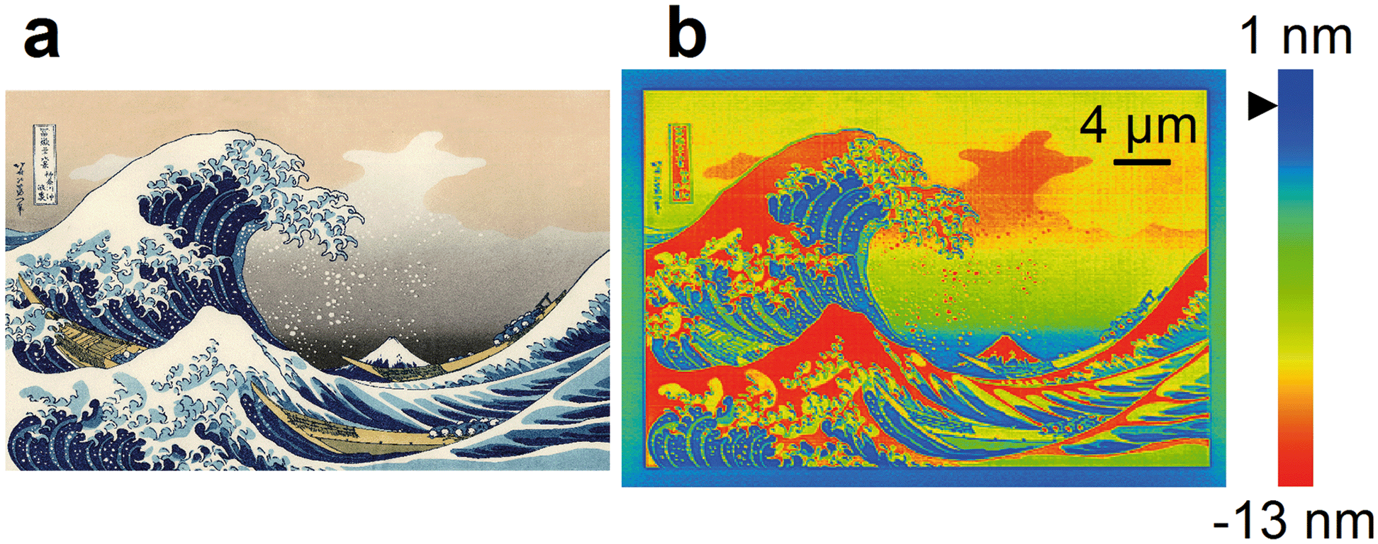 | ||
| Fig. 1 Rapid prototyping of a complex surface with subnanometer resolution of vertical dimensions by focused ion beam milling. (a) Bitmap image showing a complex pattern of arbitrary design by Hokusai. (b) Atomic force micrograph showing the same pattern in a silicon surface with 36 vertical dimensions over a range of 14 nm. The black triangle to the left of the color code indicates the zero plane, which the silicon surface swells above at low doses resulting in initial variation of vertical dimensions of a few nanometers. Fig. S3† shows a shallower version of this pattern with a vertical range of 4 nm, and describes the patterning speed. | ||
Two parameters involving the diameter of a focused ion beam and the number of pixels in a bitmap image relate our vertical and lateral dimensional control. First, the ratio of beam diameter to pixel pitch determines the beam overlap.23,24 We find that an overlap ratio of at least two can produce planar surfaces with roughness of less than 0.2 nm in silicon (100), as Fig. S4† shows, which is less than a single atomic diameter. The system magnification can induce a related aliasing artifact at subnanometer scales, as Fig. S5† shows. These results inform our subsequent selection of overlap ratios and system magnifications to pattern nominally planar surfaces. Second, an overlap ratio of two limits the pattern area or lateral range to (½)2 × (Number of pixels) × (Beam diameter)2, while the beam diameter limits the lateral resolution. We can maintain subnanometer control of vertical dimensions while decreasing the lateral resolution below 100 nm, as Fig. S6† shows, but integrating multiple patterns across large areas can result in vertical stitching errors. Circumventing these limits, we write multiple patterns in parallel, smoothly integrating their vertical dimensions at subnanometer scales for the first time in silicon (100), as Fig. S7† shows.
Silicon structures
We begin our investigation of material responses with silicon (100). The use of a focused beam of gallium ions to nanostructure silicon is a topic of ongoing research25 involving various processes that occur under ion bombardment.23,26,27 Annealing,28,29 swelling,30,31 milling,31 and sputtering over the inner plane of the pattern,9 milling and redepositing at the outer edge of the pattern,32 and backscattering33 are all relevant to the resulting nanostructure, but the resulting limits of vertical dimensional control are unknown. We first test low doses that result in a few nanometers of initial variation of vertical dimensions around the zero plane, as Fig. 2 shows. A simple bitmap image of adjacent white and black regions results in a complex superposition of these processes near a pattern edge. | ||
| Fig. 2 Investigating the vertical response of silicon to a low dose of gallium ions. (a and b) Plots showing the vertical response at the inner plane and outer edge of a patterned surface. At doses exceeding 10−2 pC μm−2, the inner plane of the patterned surface swells up measurably as silicon amorphizes. At doses from 10−1 pC μm−2 to 10−0 pC μm−2, the surface swells up to a maximum height of approximately 1.1 nm above the zero plane. By a dose of 101 pC μm−1, swelling and sputtering compensate, returning the surface to the zero plane. Sputtering silicon redeposits as a ridge at the outer edge of the patterned surface, while reflecting gallium ions mill a trench at its inner edge. Vertical bars are confidence intervals of 95%. (c–h) Representative sections of atomic force micrographs showing adjacent regions with and without exposure to increasing doses from (b). | ||
Monocrystalline silicon swells due to the implantation of gallium ions, which damages the crystal lattice27,29 and amorphizes the silicon.32,34 This amorphous layer sputters and reforms during patterning, which we view as useful, as we do not consider crystal steps35 to be practical features in complex patterns of arbitrary design. At doses exceeding 1 × 10⁻² pC μm−2, the surface swells up measurably. For this test, we deliver doses exceeding 5 × 10⁻² pC μm−2 using a dwell time of 1 μs per pixel and an increasing number of passes. At doses from 5 × 10⁻² pC μm−2 to 1 × 100 pC μm−2, the surface swells up to about 1 nm above the zero plane, reaching a maximum height of 1.11 nm ± 0.08 nm. Crystalline and amorphous silicon differ in density by between 2% and 4%,34,36 so the maximum height indicates a penetration depth of 28 nm to 56 nm for gallium ions at 30 keV. We simulate corresponding ion trajectories,37 as Table S2† reports, which we find to be informative but not predictive of the experimental limits of dimensional control.
As the dose increases from 1 × 100 pC μm−2 to 1 × 101 pC μm−2, the silicon surface returns to the zero plane and then reaches a depth of approximately 1 nm below it. These values are comparable to those of previous studies,9–11 but the transition from swelling to milling in this range depends strongly on dose rate, which we modulate by dwell time and pass number. In this range, gallium ions reflect off silicon walls to form trenches at the inner edge of the pattern, while silicon sputters and redeposits to form ridges at the outer edge. At doses of less than 5 × 101 pC μm−2, these ridges saturate at a maximum height of 10 nm above the zero plane. Neither of these edge defects is evident within patterns, and the integration method in Fig. S7† eliminates these edge defects between patterns. However, edge defects at the pattern periphery can still degrade device function, and we further mitigate them in a subsequent process of device bonding to maintain dimensional control.
We increase the dose to pattern vertical features in silicon across the nanometer scale. Fig. S8† shows the test pattern. As the dwell time and number of passes increase, the surface reaches greater depths below the zero plane, as Fig. 3a shows, first increasing linearly and then quadratically with dose, as Fig. 3b and Table S3† show. This nonlinear response becomes more prominent at depths greater than approximately 30 nm below the zero plane, which is consistent with the penetration depth of gallium ions. The initial response depends strongly on dose rate, as Fig. 3a and b, and S9† show. Longer dwell times result in more damage to the crystal lattice, while fewer passes result in less time for thermal annealing, resulting in more swelling.38 Variation of depth increment between nearest vertical dimensions for a certain dose rate is one measure of dimensional control, remaining below 0.1 nm down to approximately 10 nm below the zero plane, as Fig. 3c and Table S3† show.
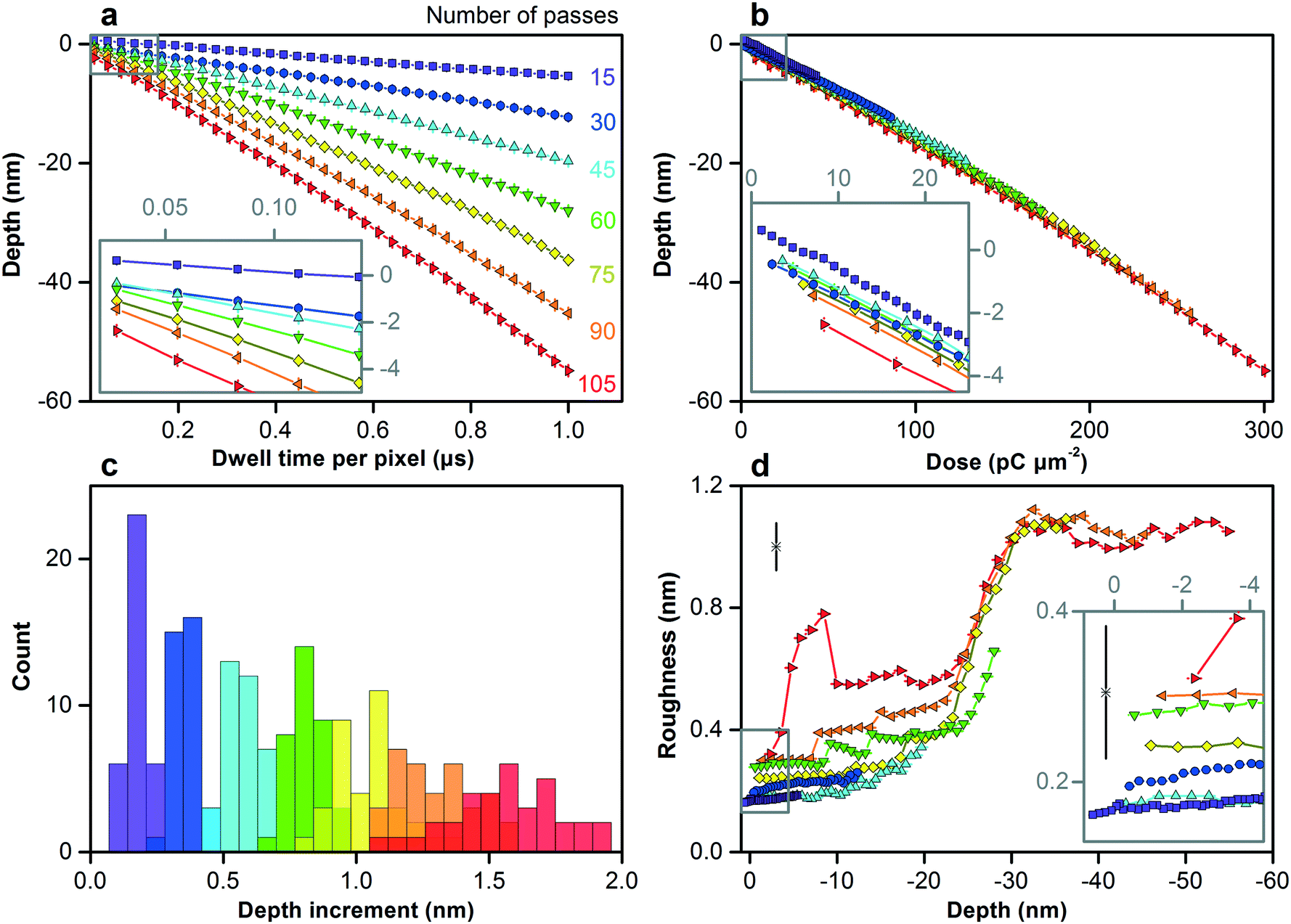 | ||
| Fig. 3 Controlling the vertical dimensions of silicon across the nanometer scale. (a–d) Plots and histograms showing different measures of vertical dimensional control. (a) Depth below the zero plane increases with both dwell time and number of passes, which we color code. (b) Depth below the zero plane increases first linearly and then quadratically with dose, as Table S3† quantifies, with the initial response (inset) depending strongly on the dose rate. (c) Subnanometer variation of depth increment, one measure of dimensional control, increases with depth. Table S3† quantifies the variation. (d) Surface roughness increases from below 0.2 nm for the smallest vertical features (inset) to a maximum of approximately 1.1 nm at a depth of approximately 60 nm below the zero plane. Horizontal and vertical bars are confidence intervals of 95%. Lone data markers in the upper left corners of (d) and inset show representative values of uncertainty. | ||
Surface roughness is another measure of dimensional control. We can mill surfaces with roughness of less than 0.2 nm down to approximately 10 nm below the zero plane, depending on dose rate, as Fig. 3d and S9c† show. The low scatter of this roughness data relative to measurement uncertainty suggests that our uncertainty evaluation, which accounts for systematic effects, is ultimately conservative. This result is potentially useful because surface roughness, depending on its spatial frequency, is not always equivalent to dimensional uncertainty, as in our application of size exclusion. Therefore, in combination with our variation of depth increment below 0.1 nm, our functional dimensional control potentially extends below 0.1 nm, which is unprecedented. Roughness peaks at shorter dwell times and greater numbers of passes, possibly due to dynamic clustering of point defects during longer annealing times.39 Around depths of 20 nm to 30 nm below the zero plane, roughness increases sharply for all dose rates and then saturates at approximately 1.1 nm. Both values are consistent with the ion penetration depth in Table S2† and the silicon swelling height, indicating an initial state of ion implantation and a transition to a steady state of milling response.
These results establish a new capability for controlling the vertical dimensions of silicon nanostructures with a focused beam of gallium ions. The stability of such nanostructures at various scales of time and temperature is a topic of interest for future study. We continue our quantitative investigation of the unknown limits of vertical dimensional control of silicon nitride and silicon dioxide for comparison and application.
Silicon nitride and silicon dioxide structures
We form a silicon nitride film with a thickness of 392 nm ± 4 nm and a silicon dioxide film with a thickness of 507 nm ± 2 nm on silicon substrates. Both materials are amorphous and the silicon nitride is stoichiometric Si3N4. Our process of patterning these materials is similar to that of silicon, but their responses differ.At low doses, silicon nitride swells up to a maximum height of approximately 1.7 nm above the zero plane, as Fig. 4a shows, which is 50% more than silicon, without a transition from a crystalline to an amorphous phase. In comparison to silicon, however, silicon nitride shows the inverse trend in response to dose rate. Silicon nitride films deflect up towards gallium ion implantation, possibly due to stress implantation.40 Longer dwell times result in higher local temperatures that increase viscoelastic flow and relieve such stress.38,41 In contrast, silicon dioxide does not swell, as Fig. 4b shows, which is consistent with its relatively low density and stress. The low sensitivity of silicon dioxide to dose rate simplifies the patterning process, which we subsequently exploit in fabricating our devices.
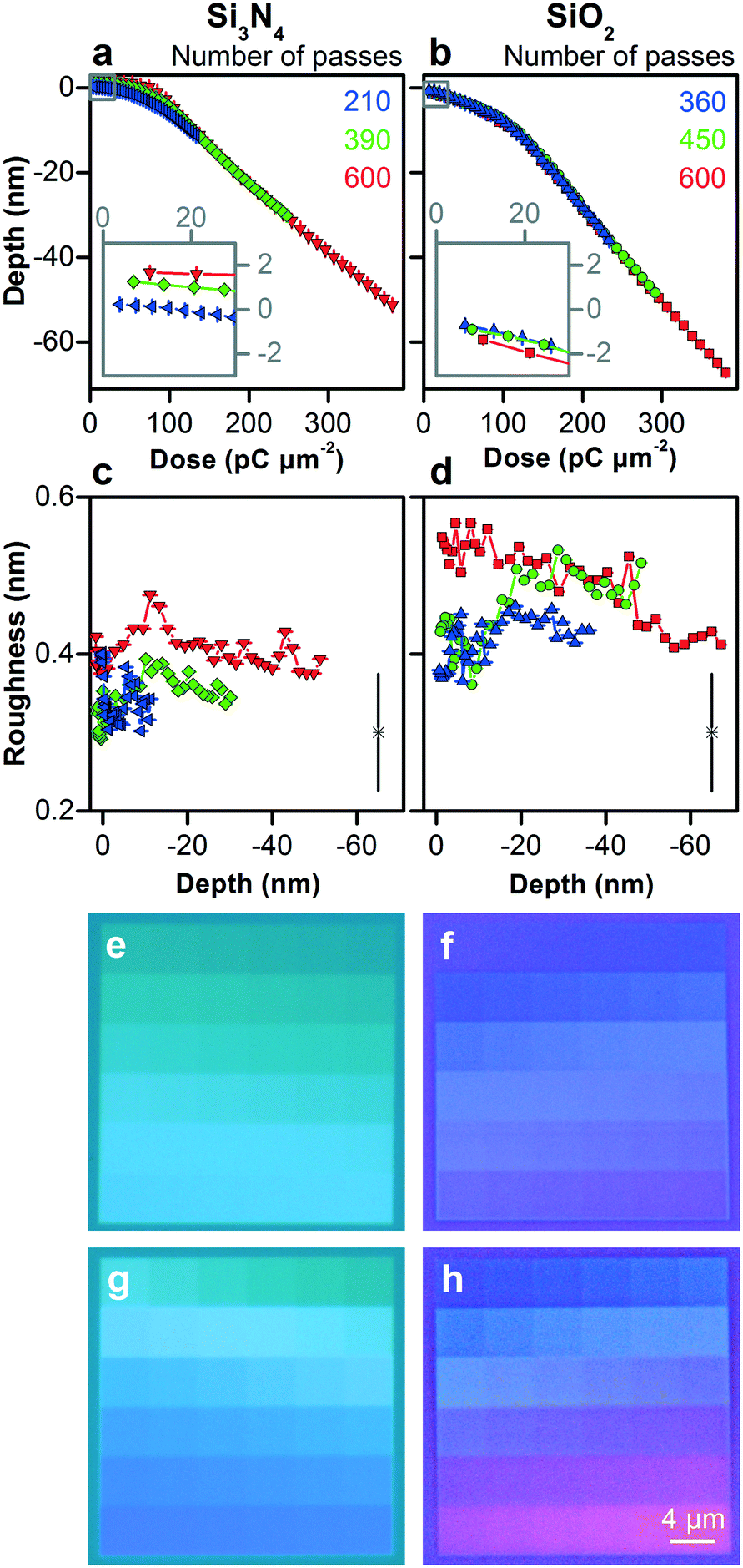 | ||
| Fig. 4 Controlling the vertical dimensions of silicon nitride and silicon dioxide across the nanometer scale. (a–d) Plots showing different measures of vertical dimensional control. (a and b) At low doses (insets), silicon nitride swells 50% more than silicon with the inverse response to dose rate, while silicon dioxide does not swell and is insensitive to dose rate. As dose increases, both materials show roughly piecewise linear responses with an inflection around 102 pC μm−2. (c and d) Surface roughness is nearly constant from 0.3 nm to 0.6 nm across the nanoscale. Horizontal and vertical bars are confidence intervals of 95%. Lone data markers at the lower right show representative values of uncertainty. (e and f) Brightfield micrographs showing test patterns corresponding to blue data in (a and c), and (b and d). (g and h) Brightfield micrographs showing test patterns corresponding to red data in (a and c), and (b and d). | ||
As dose increases, silicon nitride and silicon dioxide show responses that are roughly piecewise linear with an inflection around 102 pC μm−2. Silicon nitride shows a shallower response for the first 5 nm to 8 nm of milling, depending on dose rate, and a steeper linear response for milling across the rest of the nanoscale. Silicon dioxide shows a shallower response for the first approximately 10 nm of milling, without much dependence on dose rate, and a steeper linear response for milling across the rest of the nanoscale. The ratio of inflection depths is consistent with the ratio of penetration depths in Table S2,† although the absolute values differ by a factor of approximately three. Similar to silicon, these results indicate an initial state of ion implantation and a transition to a steady state of milling response, and demonstrate the necessity of experimental investigation of patterning responses and control limits.
The roughness of silicon nitride and silicon dioxide remains nearly constant from 0.3 nm to 0.6 nm for all depths in Fig. 4, maintaining this aspect of dimensional control throughout the patterning process, which we subsequently apply. Silicon nitride has the smoothest surfaces, possibly due to tensile stress on asperities,40 even for milling into the microscale, resulting in a remarkable ratio of milled depth to surface roughness of 5 × 10², as Fig. S10† shows.
These results demonstrate a new capability for controlling the vertical dimensions of silicon nitride and silicon dioxide nanostructures with a focused beam of gallium ions. In comparison to silicon, the different material properties result in diverse patterning responses, providing design rules for practical devices, such as those with optical and fluidic functions, as follows.
Structural colors
Submicrometer films of dielectric materials have optical properties that depend on their vertical dimensions. For example, interference of white light results in structural colors, so that subnanometer steps in film thickness are visible as color changes in Fig. 4 and S10.† These are in qualitative agreement with simulations,42 and indicate the need to calibrate for interference in the following application, which integrates and applies the preceding results.Nanofluidic devices
We scale down nanofluidic devices for the analytical separation of nanoparticles,43,44 deriving subnanometer function from structure to dramatically improve their utility. Such devices separate nanoparticles by steric interaction and size exclusion, as Fig. 5a shows, confine them within a focal volume that is nearly optimal for optical microscopy,20 and enable reference of exclusion positions to device depths to measure nanoparticle sizes. Subnanometer control of nanofluidic depths enables quantitative tests of size exclusion with subnanometer resolution, and novel measurements of the dimensional and optical properties of nanoparticles.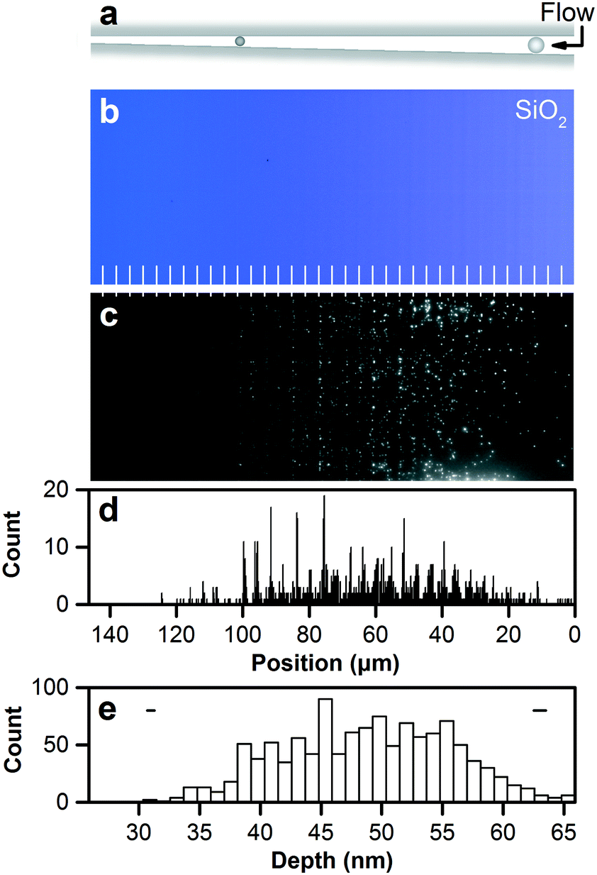 | ||
| Fig. 5 Separating and measuring nanoparticles by nanofluidic size exclusion. (a) Schematic showing size exclusion of nanoparticles in a nanofluidic staircase under a hydrodynamic flow. (b) Brightfield micrograph showing a staircase structure in silicon dioxide with 36 steps in depth from 27.6 nm ± 0.3 nm to 66.5 nm ± 0.5 nm below the zero plane. Structural colors correspond to Fig. 4f. White lines mark step edges. (c) Fluorescence micrograph showing the size separation of nanoparticles in the resulting nanofluidic staircase. The nanoparticles have a mean diameter of 48 nm and a standard deviation of 6 nm, and reach positions of size exclusion at steps that become shallower than the diameters. Surface roughness reduces milled depth by 1.2 nm to excluded depth. (d) Histogram showing nanoparticle positions of size exclusion. Position uncertainties are negligible at the scale of this plot. Reference of nanoparticle position to excluded depth places nanoparticles into bins with sizes of the depth increment or separation resolution of 1.1 nm. (e) Histogram showing corresponding excluded depths. Two horizontal bars show representative confidence intervals of 95% corresponding to minimum and maximum values of dimensional uncertainty across the nanofluidic staircase. Statistical analysis of this histogram gives the size distribution with a mean of 48.2 nm ± 2.8 nm and a standard deviation of 6.8 nm ± 0.4 nm, validating the measurement. The latter uncertainties are sampling errors. | ||
The preceding investigation informs our selection of silicon dioxide for this application, with its many useful properties of insensitivity to dose rate, highly linear response to dose at depths exceeding 10 nm below the zero plane, nearly constant roughness, lack of phase transition and greater stability against thermal annealing than silicon, and standard surface chemistry for bonding processes and nanofluidic applications. As such, we pattern our devices in a submicrometer film of silicon dioxide, as Fig. 5b shows.
Device characterization presents several interesting considerations at subnanometer scales. The staircase structure in Fig. 5b has lateral dimensions that exceed the range of our atomic force microscope. However, the highly linear response of silicon dioxide to dose in this depth range enables precise interpolation between structure depths from different micrographs in reference to the same zero plane. We seal this staircase structure with a fused silica coverslip coated with silicone resin and assume that the silicone resin absorbs any silicon dioxide asperities,45 so that milled depth exactly equals nanofluidic depth. We account for the roughness of silicon dioxide and silicone resin surfaces. Fourier analysis of Fig. S2k† shows spatial frequencies with a broad peak from 1 nm to 10 nm, while the radii of our sample nanoparticles range from less than 10 nm to more than 30 nm. Thus, surface roughness is not equal to dimensional uncertainty, and we convert nanofluidic depth to excluded depth by subtracting two standard deviations of the roughness of each surface, which is 1.2 nm. The resulting uncertainty in excluded depth varies from 0.3 nm to 0.5 nm, maintaining subnanometer dimensional control.
Analytical separation
We use polystyrene nanoparticles containing fluorescent dye to test our analytical separation. Table 1 presents the nanoparticle size distributions. We disperse the larger nanoparticles with a mean diameter of 48 nm into an aqueous buffer with a nonionic surfactant. Hydrodynamic flow transports the nanoparticles towards the shallow side of the staircase. We image the resulting size separation by fluorescence microscopy. Video S1† shows the separation process, which occurs in the dilute limit without any evident obstruction of smaller nanoparticles by larger nanoparticles, or other effects that would hinder nanoparticle transport. Fig. 5c shows the final fluorescence micrograph. Striations of nanoparticles are evident, resulting from steric interactions and size exclusion of nanoparticles at step edges where the excluded depth of the nanofluidic staircase becomes less than the nanoparticle diameter. Other nanoparticles reach positions of size exclusion at asperities between step edges and we consider these nanoparticles to correspond to that excluded depth. The depth increment of 1.1 nm defines the separation resolution and determines our ability to manipulate nanoparticles by size exclusion. This value is less than one fifth of the standard deviation of the nanoparticle size distribution.| Transmission electron microscopy | Nanofluidic size exclusion | ||||
|---|---|---|---|---|---|
| Mean value of diametera | Standard deviation of diametera | Mean value of diameterb | Standard deviation of diameterb | Number of nanoparticles | Separation resolution |
| a Nominal values are from the nanoparticle manufacturer. b Measurement uncertainties are sampling errors. | |||||
| 48 nm | 6 nm | 48.2 nm ± 2.8 nm | 6.8 nm ± 0.4 nm | 1154 | 1.1 nm |
| 24 nm | 3 nm | 25.5 nm ± 3.2 nm | 4.0 nm ± 0.5 nm | 233 | 0.6 nm |
To refer nanoparticle positions to excluded depths, we localize nanoparticles with statistical uncertainties from 8 nm to 80 nm, depending on their emission intensity. Nanoparticle striations enable localization of mean positions of step edges with uncertainties of approximately 3 nm, allowing analysis of the apparent step width in optical micrographs. This is the first such superresolution reference of nanoparticle positions to excluded depths. Fig. 5d shows a histogram of nanoparticle positions in reference to the nanofluidic staircase with a bin size of 203 nm, which is 5% of the apparent step width. Fig. 5e shows the corresponding histogram of excluded depths with a bin size of 1.1 nm, which is the depth increment and separation resolution.
To obtain the nanoparticle size distribution, we perform a statistical analysis of the histogram of excluded depths. The mean and standard deviation are each in agreement with the manufacturer specification to within an error of 1 nm, as Table 1 shows. In particular, we measure the standard deviation of the size distribution of 6 nm to within 0.8 nm. Sampling error dominates the measurement uncertainty of nanoparticle size, rather than uncertainty of device dimensions, which is interesting considering the length scale. To reduce the sampling error to the dimensional uncertainty of 0.3 nm for an excluded depth of 48 nm, we would need to measure 3 × 10⁴ nanoparticles. Each requires approximately 1 μm2 to optically resolve from other nanoparticles, so our ability to integrate subnanometer vertical features over lateral areas of 104 μm would be useful for such measurements. Alternatively, removal of single nanoparticles from optical micrographs during a time series, either through localization and analytical subtraction for stable emitters, or physical photobleaching for unstable emitters, could circumvent the diffraction limit,20 allowing superresolution imaging of analytical separation.
We scale the measurement down even further, separating smaller nanoparticles with a mean diameter of 24 nm in a nanofluidic staircase with a step depth of 0.6 nm, as Fig. S11† shows, using nearly identical methods. Again, we measure a mean and standard deviation of the size distribution that agree with the manufacturer specifications to within approximately 1 nm, as Table 1 shows. In particular, we measure the standard deviation of the size distribution of 3 nm to within 1 nm, with sampling error dominating the measurement uncertainty.
The mean error between our measurements and the manufacturer specifications of the four metrics of nanoparticle size in Table 1 is 0.9 nm, exceeding the mean uncertainty of the vertical dimensions of the nanofluidic staircase structures by a factor of approximately three. This indicates the dominance of other sources of error in the measurement, including step edge roughness and optical aberrations.46 The subnanometer agreement of nanofluidic size exclusion and transmission electron microscopy is interesting, considering the very different measurement interactions in nanofluidic confinement and under an electron beam in a vacuum system. These results establish a subnanometer limit of the fluidic manipulation of particulate matter, introduce critical-dimension particle tracking with subnanometer accuracy, and motivate future tests to determine the limit of the method at atomic scales, which our control approaches in silicon nanostructures with depths of less than 10 nm below the zero plane, as Fig. 3 shows.
Emission intensity
The size separation of fluorescent nanoparticles in a focal volume that is nearly optimal for optical microscopy enables a quantitative measure of the relationship between nanoparticle size and emission intensity. However, the excitation and emission of fluorescence from the nanoparticles are subject to interference in the dielectric films forming the device, as the structural colors of Fig. 5b indicate. We directly calibrate for interference effects by filling the nanofluidic staircase with an aqueous solution of fluorescent dye with an emission spectrum that is similar to the fluorescent nanoparticles, as Fig. 6a and S12† show. We measure the resulting values of emission intensity, subtract background noise, and normalize for excitation nonuniformity. The resulting values of fluorescence intensity vary nonlinearly with nanofluidic depth, or excluded depth, as Fig. 6b shows. Fig. 6c shows comparable values of fluorescence intensity for nanoparticles as a function of excluded depth after calibrating for the interference effect in Fig. 6b.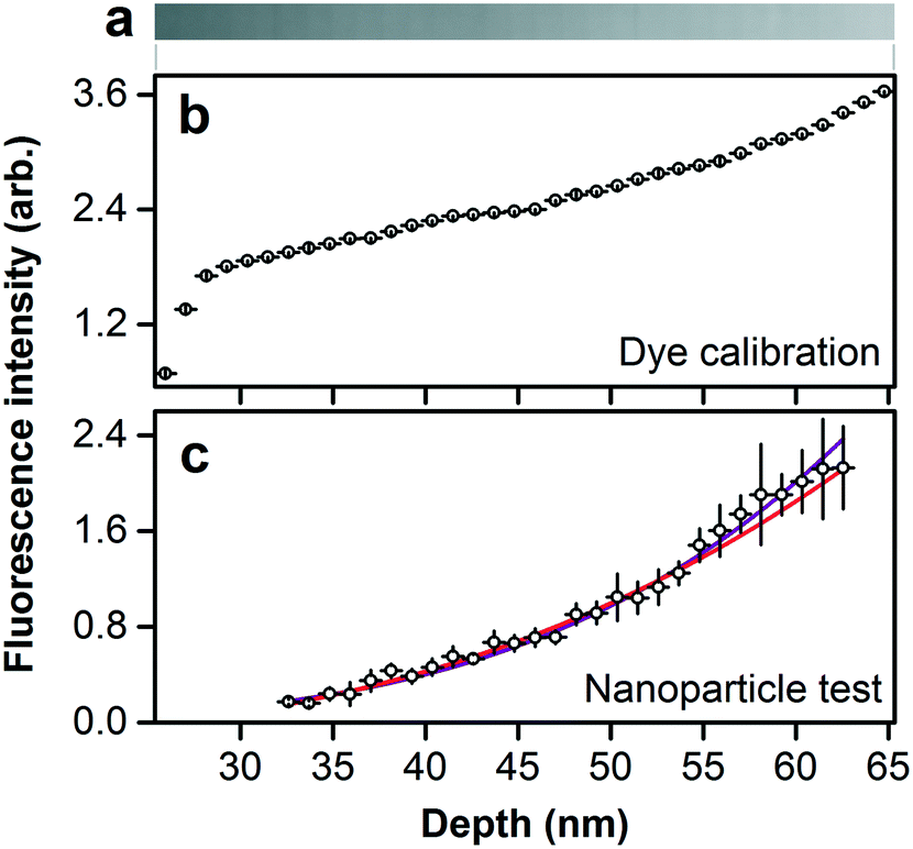 | ||
| Fig. 6 Calibrating interference effects and analyzing fluorescence intensity. (a) Fluorescence micrograph showing the emission intensity of fluorescent dye filling the nanofluidic staircase. (b) Plot showing fluorescence intensity of dye filling the nanofluidic staircase, after subtracting background noise and normalizing for nonuniform excitation. The resulting fluorescence intensity varies nonlinearly with nanofluidic depth, or excluded depth, as this plot shows for direct comparison to (c), due to optical interference. (c) Plot showing comparable values of fluorescence intensity of nanoparticles, after calibrating for the interference effect in (b). Fluorescence intensity increases with excluded depth, which is equal to nanoparticle diameter. The purple line is a fit of fluorescence intensity scaling to the fourth power of nanoparticle outer diameter. The pink line is a fit of fluorescence intensity scaling to the third power of outer diameter around an inner volume of constant diameter and lesser fluorescence intensity. Horizontal bars are limits of uncertainty, corresponding to the depth increment. Vertical bars are confidence intervals of 95%. | ||
Interpretation of the trend in Fig. 6c is not obvious. Our analysis of the manufacturer specification of the number of dye molecules in polystyrene particles with mean diameters from 20 nm to 20 μm indicates the expected volumetric scaling, as Fig. S13† shows. However, the manufacturer data for nanoparticles is insufficient to determine a trend in our size range. To quantify the relationship between fluorescence intensity IF and nanoparticle diameter D, we fit the model IF = aDb, where a and b are floating constants, to the data in Fig. 6c using the method of damped least squares, giving an adjusted R2 of 0.983 and a value of b of 4.0 ± 0.2. This exponent indicates a nonvolumetric scaling, which is unexpected.
The photobleaching of nanoparticles, as Video S1† shows, provides insight into these results. Nanoparticles of different diameters photobleach to similar levels of emission intensity, or fluorescence intensity, as Fig. S14† shows, which is also unexpected. This similarity is inconsistent with volumetric autofluorescence of polystyrene nanoparticles, and indicates the possible presence of an inner volume of fluorescent material of approximately constant diameter. Accordingly, we propose a simple empirical model for the fluorescence intensity of such nanoparticles as the result of an inner volume of constant diameter d with intensity coefficient ii, surrounded by an outer volume of variable diameter D with intensity coefficient io, with the fluorescence intensity of each component having the expected volumetric scaling,

We fit the model IF = α + βD3, where α and β are floating constants, to the data in Fig. 6c, giving an adjusted R2 of 0.985 and a negative value of α, which indicates that the inner intensity is less than the outer intensity. Such faint fluorescence could result from a variation in the inner structure of nanoparticles from the synthesis process, and the subsequent process of loading fluorescent dye through the outer surface would also affect the relationship between nanoparticle size and emission intensity. Despite the common use of such nanoparticles, and the basic importance of nanoparticle size and emission intensity in such uses, no previous study has quantified this structure–function relationship. Our surprising results are directly relevant to the manufacturers and many users of such nanoparticles, and motivate future study of their internal composition.
Conclusion
The advanced development of fabrication processes to control the lateral dimensions of complex nanostructures has resulted in great progress in many domains of nanotechnology. However, processes to control the vertical dimensions of complex nanostructures are less advanced, limiting the potential of such structures to perform useful functions. This general issue is specifically relevant to focused ion beams, due to their unique fabrication capability, as well as the ongoing development of ion sources other than gallium.5,6 Considering the fundamental importance of the relationship between structure and function in nanotechnologies with nanoscale vertical dimensions and similar or larger lateral dimensions, and that the bottom decade of the nanometer scale is largely uncontrolled and unused in such nanostructures, we have focused our attention on this open problem. Using a standard system that is broadly used but nonetheless has unexplored utility, we have demonstrated unprecedented control of the vertical dimensions of silicon, silicon dioxide, and silicon nitride at subnanometer scales by subtractive processing with a focused beam of gallium ions. Our quantitative investigation of pattern control and material responses has identified design rules for achieving this vertical resolution over a wide range of vertical and lateral dimensions, and in a broad variety of functional materials. In this way, we have enabled new control and study of structure–function relationships.In a nanofluidic application that motivates and requires this dimensional control, we have established a subnanometer limit of the fluidic manipulation of particulate matter, and introduced critical-dimension particle tracking with subnanometer accuracy. This is, to our knowledge, the most accurate optical measurement of the size of single nanoparticles in liquids. We conclude that our method presents a novel and useful combination of nanofluidic confinement and nanoparticle tracking. In comparison to other methods for directly confining nanoparticles at similar length scales, our ability to pattern complex structures enables arbitrary functions,47 and our resolution and range are record.48 In contrast to other methods of confining nanoparticles for tracking analysis, our analytical separation does not require diffusion analysis14,18 or surface functionalization,17 relying on steric interactions which are more direct and general, respectively. Further, our quantitative measurements of nanoparticle size and emission intensity have revealed a surprising relationship between these essential characteristics of common fluorescent probes, invalidating the expectation of volumetric scaling. These surprising results invite future study of other structure–function relationships and establish a firm foundation for reliable tests of the dimensional and optical properties of nanoparticles, as is necessary for quality control in medical applications.49 Our devices are also applicable to manipulate and measure biomolecules.50
Looking ahead, while we have demonstrated hydrodynamic transport of nanoparticles that is so simple as to be effectively passive, electrokinetic transport can increase the rate of analytical separation.43 In this regard, our use of a submicrometer film of silicon dioxide enables the application of high electric fields that would break down thin films of native silicon dioxide on silicon. Further, optical interference within the complex films of dielectric materials forming our devices presents challenges and opportunities for optical measurements. We can directly calibrate interference effects, as we have demonstrated, and it is also possible to minimize them. Alternatively, interference effects can enable integration of spectroscopic functions through independent control of dielectric film thickness and nanofluidic slit depth,51 and measurement of device dimensions52 with high throughput in a nanomanufacturing context.
In this last regard, we are developing reliable processes to enable the mass production of nanofluidic devices with complex structures in soft materials.53 A previous study noted the difficulty, if not impossibility, of using a focused ion beam for fabricating masters with vertical resolution below five nanometers for replica molding.54 On the basis of the results that we report here, we expect to meet this challenge. This study and another previous study35 have also demonstrated that subnanometer fidelity of pattern replication is probable. Our results provide a strong motivation to meet the next challenge of the subnanometer stability of nanofluidic devices with complex structures in soft materials.55 Indeed, our analytical separation provides a method to test both the fidelity and stability of such devices. Their optical properties will also require investigation. Autofluorescence of soft materials could limit sensitive measurements of nanoparticle fluorescence,56 while transparent devices would enable transmission darkfield microscopy of single nanoparticles.
Methods
Atomic force microscopy
We use an atomic force with a lateral range of 30 μm, a lateral position noise of less than 0.2 nm, a lateral flatness of less than 3 nm over a range of 30 μm, a vertical range of at least 3 μm, a vertical position noise of approximately 0.03 nm, a vertical noise floor of less than 0.04 nm, and an integral nonlinearity of less than 0.5%. We characterize all surfaces with silicon nitride probes with a resonant frequency of approximately 1.6 MHz and a nominal tip radius of 5 nm. We operate the atomic force microscope in tapping mode, and with a typical scan resolution of 16 nm and scan rate of 1.0 Hz. Fig. S2† shows the results of test measurements with sharper tips, higher resolution, and slower scans to evaluate uncertainties resulting from these parameters. For some of these tests, we use silicon nitride probes with a resonant frequency of approximately 82 kHz and a nominal tip radius of 2 nm. Surface features with lateral dimensions of less than 5 nm are below the typical resolution of the atomic force microscope, and below the diameter of the focused ion beam in our study. We perform atomic force microscopy within 24 h of nanostructure fabrication.Focused ion beam system
We use a focused ion beam system that operates at a pressure of less than 5 mPa and accelerates gallium cations from a liquid metal source to an energy of 30 keV. We measure the ion current to vary from 1.9 pA to 9.4 nA. The nominal ion current varies over a wider range due to wear of the aperture, which is an inherent consequence of using the system. Changing the aperture and calibrating the system are part of its routine use, motivating our use of dose as the patterning variable for primary comparison. Fig. 3 shows results from a worn aperture, for example, while Fig. S10† shows results from a new aperture. The focused ion beam impinges on the sample at normal incidence, rasters in a serpentine pattern, and rasters from regions of low to high dose for patterns with monotonic spatial variation in dose. To mill silicon nitride and silicon dioxide films, we use a scanning electron beam to compensate for charging,57,58 resulting in comparable depths for a given dose relative to silicon. Fig. S10† shows the results of milling silicon dioxide without an electron beam, which requires roughly twice the dose to mill to the same depths and results in rougher surfaces.Pattern control
We upload bitmap images in a 24-bit red–green–blue format to the focused ion beam system, which accepts bitmap images with a maximum of 1.6 × 107 pixels. The 8-bit blue value controls the dwell time of the focused ion beam.Pattern integration
We integrate multiple patterns with areas of 103 μm2 into composite patterns with areas approaching 104 μm2. For example, we integrate two staircase structures. The first staircase pattern has 18 steps with grayscale values increasing from 7 to 127 in increments of 7, and the second staircase pattern has 18 steps with grayscale values increasing from 135 to 255 in increments of 7. To integrate these staircases, the focused ion beam system takes a first pass over the first staircase pattern from top (7) to bottom (127), and then takes a sequential pass over the second staircase from top (135) to bottom (255), before returning to the first staircase pattern for a second pass. In this way, the focused ion beam system mills the two staircase patterns from top (7) to bottom (255), with a smooth interface between the two patterns at subnanometer scales, as Fig. S7† shows.Silicon substrates
We use prime-grade, p-type silicon (100) substrates, with a resistivity from 10 Ω cm to 20 Ω cm, a thickness of 525 μm, and a diameter of 100 mm.Ion penetration simulations
We simulate ion penetration using stopping and range of ions in matter (SRIM) software. We input experimental parameters as possible, using nominal density values of 2.3 g cm−3 for silicon, 3.4 g cm−3 for silicon nitride, and 2.3 g cm−3 for silicon dioxide. Table S2† shows the simulation results, with negligible statistical uncertainties.Dielectric films
We deposit a silicon nitride film onto the silicon substrates by low pressure chemical vapor deposition at a temperature of 835 °C, at a pressure of 33 Pa (0.25 Torr), with an ammonia flow rate of 120 mL min−1 (120 sccm), and with a dichlorosilane flow rate of 40 mL min−1 (40 sccm). We use stress analysis and ellipsometry to characterize the resulting film, which has a thickness of 392 nm ± 4 nm, a tensile stress of approximately 0.94 GPa, and an index of refraction of approximately 2.02 at a wavelength of 632.8 nm. We grow a silicon dioxide film by thermal oxidation in an atmospheric furnace at 1100 °C, with an oxygen flow rate of 1000 mL min−1 (1000 sccm), and with a ratio of H2 to O2 of 185%. We use ellipsometry to characterize the resulting film, which has a thickness of 507 nm ± 2 nm and an index of refraction of approximately 1.46 at a wavelength of 632.8 nm.Brightfield microscopy
We use an optical microscope with a light emitting diode to illuminate dielectric films with a broad band of wavelengths from 330 nm to 660 nm. An objective lens focuses illumination and collects light that reflects through air immersion. The objective lens has a nominal magnification of 50× or 100×, a numerical aperture of 0.95, and corrections for chromatic and flat field aberrations. A tube lens projects the image onto a color charge coupled device camera with a pixel size of 4.54 μm.Device patterning
The overall device consists of a single inlet and microfluidic channel to transport the nanoparticle suspension into the deep side of the nanofluidic staircase, and a single microfluidic channel and outlet to extract the buffer solution from the shallow side. We illustrate the device layout in Fig. S15.† We use photolithography to pattern the microfluidic features in a silicon substrate. We use an inductively coupled plasma to etch channels into the substrate, and inlets and outlets through the substrate, connecting to backside reservoirs. We spin-coat photoresist over the substrate to protect it, and dice it into chips with lateral dimensions of 20 mm × 20 mm for subsequent milling of nanofluidic devices with a focused ion beam. To pattern staircase structures with lateral dimensions of 159 μm × 62 μm, we integrate four patterns of a staircase base that underlies staircase steps, an inlet channel, and an outlet channel.Device characterization
We measure microfluidic channel depths of 0.58 μm ± 0.02 μm. The staircase structures in Fig. 5 and Fig. S11† have lateral dimensions that exceed the lateral range of our atomic force microscope. However, all of the staircase structure depths exceed 10 nm below the zero plane, and a linear fit to the corresponding range in Fig. 4b results in an adjusted R2 of 1.0000. This material response allows linear interpolation between staircase structure depths from different atomic force micrographs in reference to the same zero plane with an uncertainty that is an order of magnitude smaller than any relevant to dimensional uncertainty. This analysis gives a depth increment of 1.1 nm for the deeper staircase structure in Fig. 5, and 0.6 nm for the shallower staircase structure in Fig. S11.†Device bonding
We coat fused silica coverslips with silicone resin to bond them to silicon dioxide surfaces with milled features.45 We begin with an initial dispersion of phenyl-methylsilsesquioxane (PSQ) in methoxypropanol at a volume fraction of 20%. We dilute this initial dispersion in o-xylene to a volume fraction of 67% and filter it with an alumina membrane filter with a pore size of 0.02 μm. We clean fused silica coverslips with a thickness of 170 μm using piranha solution. We spin coat the final dispersion of phenyl-methylsilsesquioxane onto the clean coverslips at 523.6 rad s−1 (5000 RPM) for 40 s and bake them at 240 °C for 30 min. We characterize the resulting film of silicone resin using ellipsometry. The film has a thickness of 167 nm ± 1 nm and an index of refraction of 1.55 at a wavelength of 632.8 nm. We expose the silicone resin film and silicon dioxide surfaces to oxygen plasma at a pressure of 20 Pa (0.15 Torr) and a power of 50 W and the flow rate of 20 mL min−1 (20 sccm) for 1 min to terminate both surfaces with silanol groups. Contact of the surfaces at room temperature and manual pressure of less than 0.2 MPa bonds the surfaces permanently through condensation of the silanol groups. The shallower staircase has a central supporting wall with a width of approximately 650 nm, as Fig. S11† shows, as a conservative measure to prevent its potential collapse during bonding. This results in a maximum lateral dimension to vertical dimension ratio of 2.5 × 10³, which is an order of magnitude smaller than that of a previous report.45Fluorescent nanoparticles
We use fluorescent nanoparticles from a commercial manufacturer, who synthesizes the nanoparticles from a monomer and initiator in an emulsion polymerization process, resulting in spherical nanoparticles of amorphous polystyrene. The manufacturer specifies steric diameters of 48 nm ± 6 nm and 24 nm ± 3 nm, denoting the mean and standard deviation of the size distribution, from measurements of dry nanoparticles by transmission electron microscopy. After synthesis, the manufacturer disperses the nanoparticles into an organic solvent and saturates them with boron-dipyrromethene dye molecules, which are hydrophobic and electrically neutral, resulting in a peak excitation wavelength of 505 nm and a peak emission wavelength of 515 nm for the nanoparticles. The manufacturer modifies the nanoparticle surfaces with carboxylate groups with a pKa ≈ 5, resulting in a charge density of 8.6 × 101 C m−2 for the nanoparticles with a mean diameter of 48 nm, and 2.9 × 101 C m−2 for the nanoparticles with a mean diameter of 24 nm.Buffer system
We prepare a buffer system of 0.01× phosphate buffered saline containing 0.1 mM phosphate and 1.5 mM sodium chloride. We adjust the pH of the buffer to approximately 7.1 by adding hydrochloric acid and then we add a volume fraction of 0.5% of nonylphenyl-polyethylene glycol, a non-ionic surfactant. The resulting buffer has an electrostatic screening distance of approximately 8 nm. We disperse the nanoparticles into this buffer at a concentration of 1010 to 1011 nanoparticles per mL.Nanoparticle transport
We load the nanoparticle suspension into the device inlet, which initially fills by capillarity, and then a small differential of hydrostatic pressure of 6 × 101 Pa across the inlet and outlet reservoirs slowly pumps the suspension through the device. In an experiment demonstrating the nearly passive operation of the device, we wait for several hours for more than 103 nanoparticles to reach positions of size exclusion under a slow hydrodynamic flow, as Video S1† shows.Fluorescence microscopy
A light emitting diode illuminates fluorescent samples at a peak wavelength of approximately 460 nm with a half width of less than 27 nm. An excitation filter with a bandpass from 430 nm to 475 nm, a dichroic beamsplitter with a wavelength of 495 nm, and an emission filter with a bandpass from 503 nm to 548 nm discriminates between fluorescence excitation and emission. An objective lens focuses illumination and collects emission through oil immersion. The objective lens has a nominal magnification of 63×, a numerical aperture of 1.4, and corrections for chromatic and flat field aberrations. A tube lens projects the image onto a complementary metal-oxide-semiconductor camera with a pixel size of 6.5 μm. We measure the mean pixel size in fluorescence micrographs to be approximately 101 nm, using a reference structure that we mill using the focused ion beam system.Nanoparticle localization
Each subresolution nanoparticle appears as the point spread function of the fluorescence microscope. We fit a univariate Gaussian function with a constant offset for background noise to each nanoparticle image, localizing it with an uncertainty of 8 nm to 80 nm, depending on the number of photons that each nanoparticle emits. The standard deviation of the Gaussian approximation of the point spread function ranges approximately from 150 nm to 160 nm, depending on optical aberrations over the imaging field. We perform this analysis using ThunderSTORM.59 We manually cull nanoparticles at overly high areal concentrations that prevent clear interpretation of nanoparticle count and emission intensity. After analysis, we apply a Wavelet filter to background noise for clarity of presentation in Fig. 5c and S11b.† Video S1† shows a time series of unprocessed fluorescence micrographs.Reference analysis
The staircase step width has a nominal value of 3975 nm. After size exclusion, nanoparticle striations at step edges present rigid constellations of point spread functions for analysis.60 Regions of interest with widths of 0.6 μm around these striations allow localization of the mean positions of step edges within an uncertainty of 3 nm. This value combines statistical uncertainties from localization and other uncertainties from particle size. The apparent distance between step edges, after accounting for nanoparticle radii, has a mean value of 4056 nm with a standard deviation of 84 nm, with apparently wider steps toward the ends of the staircase structure. This indicates a magnification distortion of the imaging system,46 which we will revisit in a future study. In the reference of nanoparticles to steps, we account for localization uncertainty by calculating the mean uncertainty for nanoparticles in a striated constellation, corresponding to one standard deviation, and extending the effective position of each step edge towards the shallow step by two times this value of uncertainty to provide a confidence interval of 95%. Size exclusion gives nanoparticle sizes equal to the mean value of excluded depths of adjacent steps with a limit of uncertainty equal to the depth increment.Interference calibration
We fill the nanofluidic staircase with an aqueous solution of a fluorescent dye that has an emission spectrum that is similar to the fluorescent nanoparticles, as Fig. S12† shows, and also has carboxylate terminal groups. We use the same buffer from above but with a higher ionic strength of 0.1 mM phosphate and 1.0 M sodium chloride, reducing the electrostatic screening distance to approximately 0.3 nm,61 and minimizing any effects of electrostatic repulsion on filling uniformity. A high concentration of dye of 2 mM results in high values of emission intensity in fluorescence micrographs, as Fig. 6a shows. We measure the mean emission intensity of dye filling each step of the staircase from central regions with widths of at least 2 μm and lengths of at least 20 μm. We measure corresponding values of mean emission intensity from background just outside of the nanofluidic staircase and analyze their spatial variation due to nonuniform excitation intensity. We normalize this function by its maximum value to obtain a flatfield correction function. We subtract background emission intensity from dye emission intensity, and divide the resulting values by the flatfield correction function to derive fluorescence intensity in arbitrary units as a function of nanofluidic depth. Fig. 6b shows the corresponding excluded depths for direct comparison to Fig. 6c. We normalize fluorescence intensity and nanofluidic depth by dividing them by their maximum values, and calculate a ratio of normalized fluorescence intensity to normalized nanofluidic depth as an interference calibration function for the subsequent analysis of fluorescent nanoparticles. Uncertainties from this analysis are negligible in comparison to those in Fig. 6c. We express this calibration process in equation notation in Note S1.†Nanoparticle fluorescence intensity
To minimize photobleaching effects, we manually track each nanoparticle which appears in the last micrograph of Video S1† back to the first micrograph in which it appears in the time series. To measure nanoparticle emission intensity, we integrate the Gaussian fits of their point spread functions, with a local offset for constant background noise. We apply the same flatfield correction function for nonuniform excitation and divide by the interference calibration function from above to obtain directly comparable values of fluorescence intensity in arbitrary units for each nanoparticle.Fluorescence model analysis
To obtain goodness of fit metrics for our two models of emission intensity as a function of nanoparticle diameter, we perform fits using one standard uncertainty of the independent variable. In Fig. 6c, we conservatively show confidence intervals of 95% of the independent variable, and limits of uncertainty of the dependent variable. A negative value of α means that the intensity coefficient of the inner material ii is smaller than the intensity coefficient of the outer material io. Both the inner diameter and composition are unknown to us, so further analysis of the quantities ii, io, and d requires radiometric calibration of the system which is beyond the scope of this investigation.Author notes
The corresponding author will gladly provide further details of experimental procedures upon reasonable request.Conflicts of interest
The authors declare no conflicts of interest.Acknowledgements
K.-T. Liao acknowledges support of this research under the Cooperative Research Agreement between the University of Maryland and the National Institute of Standards and Technology Center for Nanoscale Science and Technology, Award 70NANB10H193, through the University of Maryland. The authors gratefully acknowledge R. Dixson for calibration of a reference material for atomic force microscopy, R. Newby for deposition and characterization of dielectric films, and J. Liddle, R. Ilic, J. Melngailis, and R. Celotta for insightful comments.References
- R. P. Feynman, Caltech. Eng. Sci., 1960, vol. 23, pp. 22–36 Search PubMed.
- L. D. Menard and J. M. Ramsey, Nano Lett., 2011, 11, 512–517 CrossRef CAS PubMed.
- K. Rykaczewski, O. J. Hildreth, C. P. Wong, A. G. Fedorov and J. H. J. Scott, Nano Lett., 2011, 11, 2369–2374 CrossRef CAS PubMed.
- K. Keskinbora, C. Grevent, U. Eigenthaler, M. Weigand and G. Schutz, ACS Nano, 2013, 7, 9788–9797 CrossRef CAS PubMed.
- H. Kollmann, X. Piao, M. Esmann, S. F. Becker, D. Hou, C. Huynh, L.-O. Kautschor, G. Bösker, H. Vieker, A. Beyer, A. Gölzhäuser, N. Park, R. Vogelgesang, M. Silies and C. Lienau, Nano Lett., 2014, 14, 4778–4784 CrossRef CAS PubMed.
- A. I. Kuznetsov, A. E. Miroshnichenko, Y. H. Fu, V. Viswanathan, M. Rahmani, V. Valuckas, Z. Y. Pan, Y. Kivshar, D. S. Pickard and B. Luk'yanchuk, Nat. Commun., 2014, 5, 3104 Search PubMed.
- M. Melli, A. Polyakov, D. Gargas, C. Huynh, L. Scipioni, W. Bao, D. F. Ogletree, P. J. Schuck, S. Cabrini and A. Weber-Bargioni, Nano Lett., 2013, 13, 2687–2691 CrossRef CAS PubMed.
- C.-S. Kim, S.-H. Ahn and D.-Y. Jang, Vacuum, 2012, 86, 1014–1035 CrossRef CAS.
- L. Frey, C. Lehrer and H. Ryssel, Appl. Phys. A: Mater. Sci. Process., 2003, 76, 1017–1023 CrossRef CAS.
- B. D. Huey and R. M. Langford, Nanotechnology, 2003, 14, 409–412 CrossRef CAS.
- A. Lugstein, B. Basnar, J. Smoliner and E. Bertagnolli, Appl. Phys. A: Mater. Sci. Process., 2003, 76, 4 Search PubMed.
- A. R. Hall, Microsc. Microanal., 2013, 19, 740–744 CrossRef CAS PubMed.
- L. Fang, N. Gogneau, J. L. Oudar, E. Bourhis and J. Gierak, Microelectron. Eng., 2014, 129, 12–16 CrossRef CAS.
- N. Mojarad and M. Krishnan, Nat. Nanotechnol., 2012, 7, 448–452 CrossRef CAS PubMed.
- J.-L. Fraikin, T. Teesalu, C. M. McKenney, E. Ruoslahti and A. N. Cleland, Nat. Nanotechnol., 2011, 6, 308–313 CrossRef CAS PubMed.
- B. H. Wunsch, J. T. Smith, S. M. Gifford, C. Wang, M. Brink, R. L. Bruce, R. H. Austin, G. Stolovitzky and Y. Astier, Nat. Nanotechnol., 2016, 11, 936–940 CrossRef CAS PubMed.
- S. Block, B. J. Fast, A. Lundgren, V. P. Zhdanov and F. Hook, Nat. Commun., 2016, 7, 8 Search PubMed.
- C. Haiden, T. Wopelka, M. Jech, F. Keplinger and M. J. Vellekoop, Langmuir, 2014, 30, 9607–9615 CrossRef CAS PubMed.
- O. S. Wolfbeis, Chem. Soc. Rev., 2015, 44, 4743–4768 RSC.
- P. P. Mathai, J. A. Liddle and S. M. Stavis, Appl. Phys. Rev., 2016, 3, 011105 Search PubMed.
- J. A. Kramar, R. Dixson and N. G. Orji, Meas. Sci. Technol., 2011, 22, 024001 CrossRef.
- R. Dixson, N. G. Orji, C. D. McGray, J. Bonevich and J. Geist, J. Micro/Nanolithogr., MEMS, MOEMS, 2012, 11, 011006 CrossRef.
- A. A. Tseng, J. Micromech. Microeng., 2004, 14, R15–R34 CrossRef CAS.
- J. Han, H. Lee, B.-K. Min and S. J. Lee, Microelectron. Eng., 2010, 87, 1–9 CrossRef CAS.
- C. Li, L. Zhao, Y. Mao, W. Wu and J. Xu, Sci. Rep., 2015, 5, 8236 CrossRef CAS PubMed.
- L. A. Giannuzzi, B. I. Prenitzer and B. W. Kempshall, in Introduction to Focused Ion Beams – Instrumentation, Theory, Techniques and Practice, ed. L. A. Giannuzzi, Springer, 2005, ch. 2, pp. 13–52 Search PubMed.
- C. A. Volkert and A. M. Minor, MRS Bull., 2007, 32, 389–399 CrossRef CAS.
- C. R. Musil, J. Melngailis, S. Etchin and T. E. Haynes, J. Appl. Phys., 1996, 80, 3727–3733 CrossRef CAS.
- P. H. Albarede and H. J. Lezec, Transmission electron microscopy of focused ion beam induced damage at 50 keV in Si, IOP Publishing Ltd, Bristol, 1998 Search PubMed.
- C. Lehrer, L. Frey, S. Petersen and H. Ryssel, J. Vac. Sci. Technol., B, 2001, 19, 2533–2538 CAS.
- A. Lugstein, B. Basnar, G. Hobler and E. Bertagnolli, J. Appl. Phys., 2002, 92, 4037–4042 CrossRef CAS.
- S. Rajsiri, B. W. Kempshall, S. M. Schwarz and L. A. Giannuzzi, Microsc. Microanal., 2002, 8, 50–51 CrossRef PubMed.
- T. L. Matteson, S. W. Schwarz, E. C. Houge, B. W. Kempshall and L. A. Giannuzzi, J. Electron. Mater., 2002, 31, 33–39 CrossRef CAS.
- J. S. Custer, M. O. Thompson, D. C. Jacobson, J. M. Poate, S. Roorda, W. C. Sinke and F. Spaepen, Appl. Phys. Lett., 1994, 64, 437–439 CrossRef CAS.
- S. Elhadj, R. M. Rioux, M. D. Dickey, J. J. DeYoreo and G. M. Whitesides, Nano Lett., 2010, 10, 4140–4145 CrossRef CAS PubMed.
- M. Koster and H. M. Urbassek, Phys. Rev. B: Condens. Matter Mater. Phys., 2000, 62, 11219–11224 CrossRef CAS.
- J. F. Ziegler, M. D. Ziegler and J. P. Biersack, Nucl. Instrum. Methods Phys. Res., Sect. B, 2010, 268, 1818–1823 CrossRef CAS.
- M. L. Brongersma, E. Snoeks, T. van Dillen and A. Polman, J. Appl. Phys., 2000, 88, 59–64 CrossRef CAS.
- S. Roorda, W. C. Sinke, J. M. Poate, D. C. Jacobson, S. Dierker, B. S. Dennis, D. J. Eaglesham, F. Spaepen and P. Fuoss, Phys. Rev. B: Condens. Matter Mater. Phys., 1991, 44, 3702–3725 CrossRef CAS.
- Y. R. Kim, P. Chen, M. J. Aziz, D. Branton and J. J. Vlassak, J. Appl. Phys., 2006, 100, 104322 CrossRef PubMed.
- D. A. Woodford, J. Am. Ceram. Soc., 1998, 81, 2327–2332 CrossRef CAS.
- J. Henrie, S. Kellis, S. M. Schultz and A. Hawkins, Opt. Express, 2004, 12, 1464–1469 CAS.
- S. M. Stavis, J. Geist and M. Gaitan, Lab Chip, 2010, 10, 2618–2621 RSC.
- S. M. Stavis, E. A. Strychalski and M. Gaitan, Nanotechnology, 2009, 20, 165302 CrossRef PubMed.
- J. Gu, R. Gupta, C. F. Chou, Q. H. Wei and F. Zenhausern, Lab Chip, 2007, 7, 1198–1201 RSC.
- C. R. Copeland, C. D. McGray, J. Geist, V. A. Aksyuk, J. A. Liddle, B. R. Ilic and S. M. Stavis, 2017, arXiv:1710.09803.
- S. R. Leslie, A. P. Fields and A. E. Cohen, Anal. Chem., 2010, 82, 6224–6229 CrossRef CAS PubMed.
- M. N. Hamblin, J. Xuan, D. Maynes, H. D. Tolley, D. M. Belnap, A. T. Woolley, M. L. Lee and A. R. Hawkins, Lab Chip, 2010, 10, 173–178 RSC.
- L. K. Bogart, G. Pourroy, C. J. Murphy, V. Puntes, T. Pellegrino, D. Rosenblum, D. Peer and R. Levy, ACS Nano, 2014, 8, 3107–3122 CrossRef CAS PubMed.
- S. M. Stavis, J. Geist, M. Gaitan, L. E. Locascio and E. A. Strychalski, Lab Chip, 2012, 12, 1174–1182 RSC.
- F. Westerlund, F. Persson, A. Kristensen and J. O. Tegenfeldt, Lab Chip, 2010, 10, 2049–2051 RSC.
- D. Berard, C. M. J. McFaul, J. S. Leith, A. K. J. Arsenault, F. Michaud and S. R. Leslie, Rev. Sci. Instrum., 2013, 84, 103704 CrossRef PubMed.
- T. P. Kole, K.-T. Liao, D. Schiffels, B. R. Ilic, E. A. Strychalski, J. G. Kralj, J. A. Liddle, A. Dritschilo and S. M. Stavis, J. Res. Natl. Inst. Stand. Technol., 2015, 120, 252 CrossRef PubMed.
- Q. Xu, B. T. Mayers, M. Lahav, D. V. Vezenov and G. M. Whitesides, J. Am. Chem. Soc., 2005, 127, 854–855 CrossRef CAS PubMed.
- Y. Y. Huang, W. Zhou, K. J. Hsia, E. Menard, J.-U. Park, J. A. Rogers and A. G. Alleyne, Langmuir, 2005, 21, 8058–8068 CrossRef CAS PubMed.
- S. M. Stavis, Lab Chip, 2012, 12, 3008–3011 RSC.
- J. Benawra, A. M. Donald and M. Shannon, J. Microsc., 2009, 234, 89–94 CrossRef CAS PubMed.
- D. J. Stokes, T. Vystavel and F. Morrissey, J. Phys. D: Appl. Phys., 2007, 40, 874–877 CrossRef CAS.
- I. Izeddin, J. Boulanger, V. Racine, C. G. Specht, A. Kechkar, D. Nair, A. Triller, D. Choquet, M. Dahan and J. B. Sibarita, Opt. Express, 2012, 20, 2081–2095 CrossRef CAS PubMed.
- C. McGray, C. R. Copeland, S. M. Stavis and J. Geist, J. Microsc., 2016, 263, 238–249 CrossRef CAS PubMed.
- X. Lin, Q. Yang, L. Ding and B. Su, ACS Nano, 2015, 9, 11266–11277 CrossRef CAS PubMed.
Footnote |
| † Electronic supplementary information (ESI) available. See DOI: 10.1039/c7lc01047h |
| This journal is © The Royal Society of Chemistry 2018 |