
 Open Access Article
 This Open Access Article is licensed under a
 Creative Commons Attribution 3.0 Unported Licence
Asymmetric nanofluidic grating detector for differential refractive index measurement and biosensing†
F.
Purr
 ab,
M.
Bassu
b,
R. D.
Lowe
b,
B.
Thürmann
a,
A.
Dietzel
*a and
T. P.
Burg
*b
ab,
M.
Bassu
b,
R. D.
Lowe
b,
B.
Thürmann
a,
A.
Dietzel
*a and
T. P.
Burg
*b
aTU Braunschweig, Institute of Microtechnology, 38124 Braunschweig, Germany. E-mail: a.dietzel@tu-braunschweig.de
bMax Planck Institute for Biophysical Chemistry, 37077 Göttingen, Germany. E-mail: tburg@mpibpc.mpg.de
First published on 24th October 2017
Abstract
Measuring small changes in refractive index can provide both sensitive and contactless information on molecule concentration or process conditions for a wide range of applications. However, refractive index measurements are easily perturbed by non-specific background signals, such as temperature changes or non-specific binding. Here, we present an optofluidic device for measuring refractive index with direct background subtraction within a single measurement. The device is comprised of two interdigitated arrays of nanofluidic channels designed to form an optical grating. Optical path differences between the two sets of channels can be measured directly via an intensity ratio within the diffraction pattern that forms when the grating is illuminated by a collimated laser beam. Our results show that no calibration or biasing is required if the unit cell of the grating is designed with an appropriate built-in asymmetry. In proof-of-concept experiments we attained a noise level equivalent to ∼10−5 refractive index units (30 Hz sampling rate, 4 min measurement interval). Furthermore, we show that the accumulation of biomolecules on the surface of the nanochannels can be measured in real-time. Because of its simplicity and robustness, we expect that this inherently differential measurement concept will find many applications in ultra-low volume analytical systems, biosensors, and portable devices.
1 Introduction
Refractive index is a fundamental quantity, intrinsic to the physical and chemical properties of a substance. Measurements of refractive indices are widely used in the pharmaceutical industry,1 environmental monitoring,2 adulteration detection,3–5 and biosensing.6–10 Several technologies for refractive index measurement have been previously described in the literature, and with the push for further miniaturization, many microfluidic technologies have emerged. A brief summary of these methods is outlined in Table 1.| Technology | Detection limit | Background cancelation/self-referencing | Size/volume | Ref. |
|---|---|---|---|---|
| Surface plasmon resonance | 1 × 10⁻⁷–2 × 10⁻⁵ RIU | No | 20–150 μL (ref. 24) | 24, 25 |
| Young interferometer | 1.8 × 10⁻⁸ RIU (ref. 26) | Yes, reference arm | 6 μL (ref. 26) | 26–29 |
| Microinterferometric backscatter detector | 6.9 × 10⁻⁹ RIU | Yes, two capillaries: fringe subtraction | 50 nL | 30 |
| Ring resonator | 3.16 × 10⁻⁶ RIU (ref. 31) | Independent reference structures: multiple sensors on one chip with beam splitter33 yes, double resonator34 | 200 × 20 μm/10 μL min−1 (ref. 33) resonator cross section: 68 μm (ref. 32) | 31–34 |
| 3.8 × 10⁻⁸ RIU (ref. 32) | ||||
| 5.0 × 10⁻⁶ RIU (ref. 33) | ||||
| Fiber Bragg grating | 2.2 × 10⁻⁵ RIU | No | 3.45 μm per hole | 35, 36 |
| Fabry–Perot cavity | 1.7 × 10⁻⁵ RIU (ref. 37) | No | Cavity width = 24.5 μm (ref. 37) | 37–43 |
| Photonic crystal: nanoscaled optofluidic sensor array (NOSA) | 7 × 10⁻⁵ RIU | Independent reference structures: multiple sensor structures on one chip with one waveguide | Hole diameter 200 nm, 250 nm deep, 8 holes per sensor | 44 |
| Diffraction grating | 1.9 × 10⁻⁶ RIU (ref. 45 and 46) | I0 as reference | 50 μm thick fluid layer47 | 45–47 |
| 6 × 10⁻⁷ RIU (ref. 47) | ||||
| Micro edge | 3 × 10⁻³ RIU | No | 20 μm deep; 250 μm wide | 48 |
| μ-Image defocusing 3-pinhole aperture | 53.7 pixel per RIU | Self-calibration: reference fluids included on chip – one image measurement | 50 μm wide; 17–82 μm deep | 49 |
| Tapered fiber | 1.42 × 10⁻⁵ RIU (ref. 50) | No | Diameter of fiber 200 μm; 6 mm long9 | 9, 50 |
For many applications, there is a need to measure small changes in refractive index that are easily overwhelmed by nonspecific background signals. For example, measurements of concentration via refractive index require accurate temperature control, and refractive index based biosensors need to be made insensitive to non-specific binding or bulk refractive index changes. Differential measurements with two devices offer a partial remedy. However, the attainable background suppression is often limited due to alignment errors, fabrication tolerances, and other differences between independent sensors.
Diffractive optical microdevices open up a path to differential sensing with direct background cancellation by the interference of light waves. One key advantage of these devices is that the signal of interest and the reference are closely integrated and lie on the same beam path. This principle has previously been used for displacement sensing in micromechanics,11–13 for chemical sensing,14–17 and for biosensing.18–20 In chemical and biological sensing, many powerful device concepts have been proposed based on micropatterning capture molecules or hydrogels into stimulus-responsive phase gratings.18,21 Binding of target molecules or swelling of the hydrogel alters the wavefront of a laser passing through the element, and this can be read out via a consequent change of the diffraction pattern in the far-field. Multiplexing is also possible by this principle if multiple gratings with different orientation are overlaid.22,23
Here, we introduce a new diffractive optofluidic device for measuring small differences in refractive index between two fluids that are guided through nanofluidic channels. The device consists of two sets of nanochannels, which are arrayed to form an interdigitated grating with an asymmetric unit cell. We show for the first time that the asymmetry enables linear optical differencing in diffractive sensors even when the optical layer thicknesses (here the nanochannel depths) are fixed and cannot be adjusted to achieve phase quadrature.
Using this device, it is possible to measure small differences in the bulk refractive index of two solutions in the presence of large common-mode fluctuations. Alternatively, the device can measure optical path differences caused by different surface-adsorbed layers. This effect is significant due to the small height of our nanofluidic channels. We envision that the inherently differential measurement and the efficient surface-directed transport of molecules in the nanofluidic channels render this concept interesting for label-free biosensing applications.
1.1 Optofluidic grating design and theory
A schematic representation of the nanofluidic diffraction grating device where reference and detection nanochannels are placed in an asymmetric interdigitating arrangement is shown in Fig. 1. The asymmetric unit cell of the grating results in the formation of a diffraction pattern which is not mirror-symmetric (I−m ≠ Im) Fig. 1B. Importantly, this asymmetric distribution is produced only when the refractive indices in the reference (yellow) and in the detection channels (green) are different Δn = nRef − nDet ≠ 0. This allows changes in the refractive index within the detection nanochannels to be detected by measuring the difference in intensity ΔIm = Im − Im.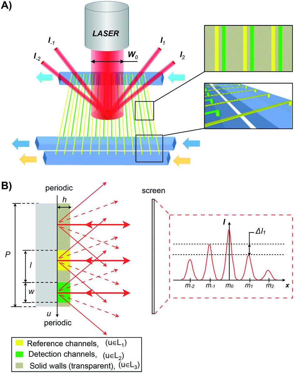 | ||
| Fig. 1 A) Schematic showing the nanofluidic diffraction grating with an asymmetric arrangement of detection and reference nanochannels. Open vias connect each nanochannel to the larger supply microchannels. B) Cross-sectional schematic view of a single grating period. This grating reflects the incident coherent optical beam into several orders with an intensity profile that depends on the geometric parameters of the grating and on the refractive index of the fluid in the detection and reference nanochannels. | ||
For a correct signal processing, we calculate here the dependence of the intensity distribution of the diffraction pattern produced by the asymmetric grating for small Δn.
When a collimated laser beam is reflected off the device, the reflected light intensity in the Fraunhofer approximation at a distance D from the chip is given by:11,51
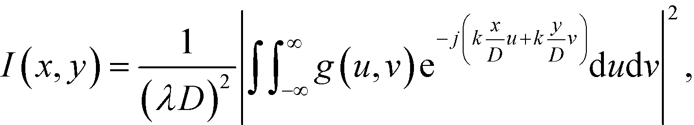 | (1) |
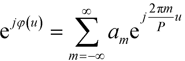
 and the aperture function g(u,v) represents the complex field amplitude of the reflected beam in the plane of the device. The aperture function can be expressed as
| g(u,v) = f(u,v)·ejφ(u), | (2) |
 | (3) |
 | (4) |
Inserting eqn (2) into eqn (1) and using the convolution theorem, we find the diffraction pattern to be a linear array of peaks located at positions 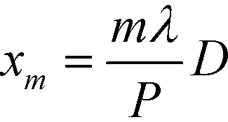 . If f(u,v) is a Gaussian beam of waist diameter W0 ≫ P, then all the peaks are also Gaussian in shape, well separated, and non-interfering.
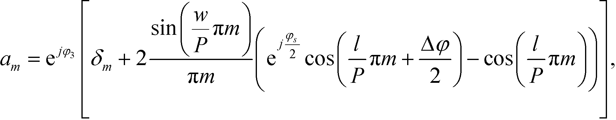
The peak intensities are proportional to the magnitudes of the coefficients am:
| Im ∼ |am|2. | (5) |
Here we define the signal of our measurement for a pair of modes m ≠ 0 as
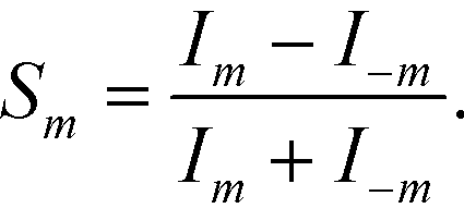 | (6) |
This is a non-linear function of the refractive indices of the fluids inside the detection and the reference channels. Expanding to the first order in Δφ reveals that, for small optical path differences,
 | (7) |
Importantly, Sm is independent of the absolute optical path length in the reference and detection channels provided that Δφ ≪ 1. Also note that, to first order, the sensitivity 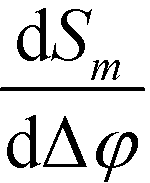 is independent of the channel width. This is due to the normalization by the total mode intensity Im + I−m which tends towards zero for w → 0. Analogously, the optical path φ3 through the wall between the channels does not enter into the linear approximation of the normalized signal. Note that the parameters w and φ3 can still be used to optimize the amount of light diverted from the central peak (m = 0) to higher order modes. While the divergence of the tangent in eqn (7) for arguments approaching odd multiples of
  suggests a very large sensitivity at these points, there is a trade-off in signal-to-noise ratio, for the net mode intensity tends towards zero at the same time, as revealed by eqn (4).
Of particular interest is that  and the channel depth h are the only design parameters entering into eqn (7). For a symmetric arrangement
 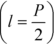 of reference and detection channels in the array we find
  for all even values of m. In this special case, the diffraction pattern is symmetric about the origin. Each diffracted mode is then either at a maximum or at a minimum of intensity when Δφ = 0 due to complete constructive or destructive interference between the light reflected off the reference and the detection channels, respectively. For all other values of l, the operating point of the interferometer acquires a desirable bias away from these points of zero sensitivity. This is critical for many sensing applications that require the measurement of rather small differences in refractive index around Δn = 0.
1.2 Fabrication
The nanofluidic grating sensor was fabricated using standard microfabrication techniques as shown in Fig. 2. Silicon-on-insulator (SOI) wafers were initially dry thermally oxidized to a depth of 290 nm. Nanochannels were then formed on the SiO2 top layer using photolithography and buffered hydrofluoric acid (BHF) wet etching. The silicon device layer of the SOI wafer acted as an etch stop, resulting in a nanochannel depth (h) equal to the thickness of the SiO2 layer. The small channel depth of only 290 nm has the significant advantages of requiring a low volume of sample (only 14 pL), a high contribution of the surface layer to the channel refractive index, and a small diffusion length. All these elements make it possible to use the device to detect binding of molecules in short time frames. On the other hand, the small channel depth has also the drawback of making the exchange of high-viscosity fluids challenging. High pressure would be necessary to push such fluids through the nanochannels.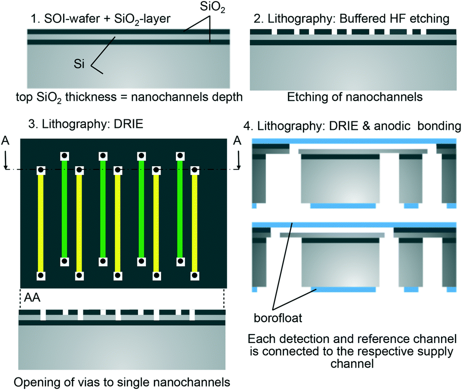 | ||
| Fig. 2 Schematic of the fabrication process for the nanofluidic assymmetric grating device. | ||
For the lateral dimensions of the nanochannels, we selected two combinations: (1) w = 3 μm, l = 7 μm, P = 18 μm and (2) w = μm, l = 6 μm, P = 18 μm. These dimensions were chosen to obtain high sensitivity to bulk refractive index changes and to surface-adsorption while maintaining safe tolerances during fabrication. The grating layout consisted of 25 reference and detection nanochannels, respectively, for a total of 50 channels per grating, and each channel was 320 μm in length. Vias (3 μm in diameter) on each end of the nanochannels were opened by deep reactive ion etching (DRIE) through the silicon device layer of the SOI followed by BHF to open the buried oxide (Fig. 3A).
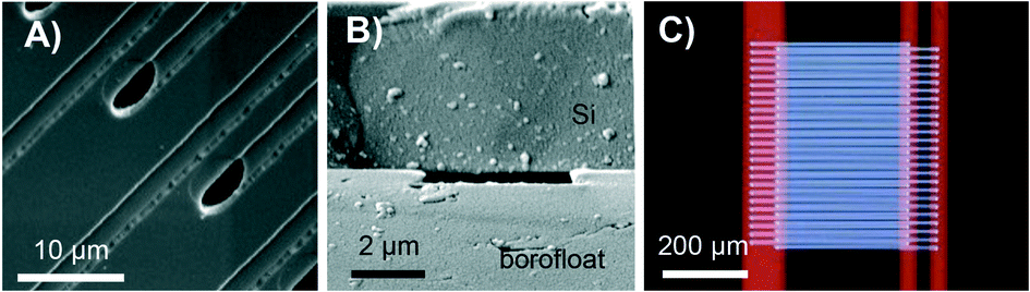 | ||
| Fig. 3 A) SEM top tilted view of open nanochannels and supply vias. B) SEM cross sectional view of a 290 nm deep nanochannel after glass wafer bonding to SOI wafer. C) Optical top view image of the nanofluidic grating. The transmission of light through the 4 μm thick silicon device layer gives the red coloration to the back side feeding channels. | ||
Subsequently, a 210 μm thick Borofloat 33 wafer was bonded to the top side of the silicon wafer to seal the nanofluidic grating. The silicon wafer was then ground to a thickness of 50 μm and polished. After the silicon was thinned down, microfluidic channels were etched from the back side by DRIE to connect to the vias previously fabricated from the top side. After bonding, a thin residual oxide diaphragm that sometimes remained in the vias was cleared by a vapor-phase HF etch. Thinning the silicon served a dual role in the above process. First, the depth and aspect ratio of the DRIE step was significantly reduced; thus, the etch could be stopped uniformly and with minimal footing on the buried oxide layer of the SOI. Second, the volume of the microfluidic channels connecting to the nanochannels could be kept small in this way.
Finally, a 700 μm thick Borofloat 33 wafer was bonded onto the back side of the wafer to ensure the robustness of the fabricated devices. Before bonding, through-holes (800 μm in diameter) were opened on the back side Borofloat 33 wafer by femtosecond laser ablation to allow fluid delivery into the nanofluidic system.
The use of silicon and glass as substrate results in the fabrication of robust and chemically resistant chips. This, on the other hand, requires a relatively expensive fabrication technology. An alternative could be the use of thermoplastic materials and hot embossing that would allow fabricating disposable devices more suitable for point-of-care applications.
1.3 Optical and fluidic setup
The diffraction pattern that is generated when a collimated laser beam (λ = 635 nm, waist diameter 360 μm) impinges on the nanofluidic grating is reflected back onto a mirror and into a CCD camera (Thorlabs DCU223M or Andor iXon Ultra). The signal intensity of each maximum (I±m) is measured by integrating the gray values over an area large enough to include all of the signal.A pressure-driven fluidic system was used to introduce fluids into all channels. The reference and detection nanochannels can be supplied with different fluids through separate microfluidic supply channels (Fig. 1 and 3C), enabling selective functionalization and avoiding contamination between the channels. The fluids are guided through the nanochannels by controlling the pressures on either side.
Additional details regarding the optical and fluidic setup are described in the ESI.†
For each measurement, a baseline was determined by flushing all channels with the reference solution (water or PBS for these studies) for five minutes. At the five minute interval, the pressure difference was switched to introduce the sample solution into only the detection channel and reference solution was maintained in the reference channel. Following the measurement, all channels in the grating were again filled with the reference solution. To avoid clogging of the nanochannels, all solutions were passed through a 300 kDa cutoff filter before use.
2 Results and discussions
2.1 Device characterization
To validate our theoretical model, we conducted calibration measurements using glycerol solutions in DI water in the concentration range of 1–30% (w/w), equivalent to a refractive index range of n = 1.334–1.373. The refractive index of glycerol depends strongly on the solution concentration.52 All glycerol solutions were also characterized with a pocket refractometer (Atago USA, Inc.) prior to analysis with our new method. For each measurement, all channels were initially filled with DI water, and the resulting signal was taken as a baseline. When the glycerol solution was then introduced into the detection channels at around 4 minutes, the difference in refractive index between detection and reference channels resulted in a change in the signal S2 (Fig. 4A). The second maximum (m = 2) were used because, for the chosen geometry, they show the higher intensity after the 0th maximum.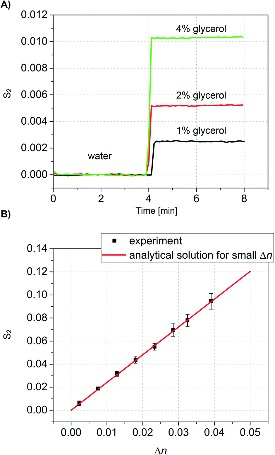 | ||
| Fig. 4 A) Plot of the signal S2 as a function of the measurement time. A sudden change in S2 is observed when the glycerol solution is introduced into the detection nanochannels. n = 1.334 (1% glycerol), n = 1.335 (2% glycerol), n = 1.377 (4% glycerol) B) experimental calibration curve and analytical solution for small Δn as a function of Δn. (device dimensions w = 3 μm, l = 4 μm, P = 18 μm). | ||
The same procedure was then repeated in triplicate for every concentration of glycerol, thus demonstrating the repeatability of the measurements and stability of the system. In all measurements the same baseline was recovered when water was again introduced into the detection channels.
Values of S2 are plotted as a function of the independently measured Δn in Fig. 4B. For comparison, Fig. 4B also shows the theoretical prediction calculated according to eqn (7). The slope s = ∂S2/∂Δn corresponds to the sensitivity of our device. Based on the geometry and the wavelength we find s = 2.408 RIU−1. Importantly, the linear response of the sensor corresponds accurately with the analytical solution for the entire range of Δn measured. Linear regression on the data shown in Fig. 4B yields a slope ŝ = 2.416 ± 0.01926 RIU−1 (correlation coefficient of R = 0.99954). This is in good agreement with the analytical prediction.
The noise floor is dominated by low-frequency fluctuations. Over the first four minutes of measurement, the refractive index equivalent of the standard deviation in S2 is σΔn = 1.3 × 10⁻⁵ RIU. For comparison with other methods that are summarized in Table 1, our limit of detection taken as three standard deviations above the noise corresponds to ∼4 × 10⁻⁵ RIU.
2.2 Common mode rejection analysis
The accuracy of refractive index measurements can be significantly affected by temperature fluctuations. Here, we show that the differential design of our sensor greatly reduces the influence of thermal drift on the measurement result. Fig. 5 shows an experiment where common refractive index changes due to temperature changes are efficiently suppressed. The experiment is divided into four phases. In the first phase, the temperature of the device was set to 25 °C and DI water was introduced into both channel types. In the second phase, a 2% glycerol solution was introduced into only the detection nanochannels. This induced a decrease in both intensities I−2 (black) and I+2 (orange). A Δn = 0.0025 was calculated starting from the measured S2 using the experimentally determined sensitivity of 2.416/ΔRIU. In the third phase, the temperature of the device was increased by 8 °C inducing a change in the refractive index in both reference and detection channels. Although this can be noted as an increase in the individual mode intensities I+2 and I−2, the effect of the temperature change is significantly suppressed in the measured Δn. A small decrease of Δn of about 2 × 10⁻⁴ RIU was measured in the third phase, around an order of magnitude smaller than the expected refractive index change induced in water from an 8 °C increase in temperature.53 In the fourth phase, water was introduced again to the detection channel, and the measured Δn subsequently decreased back to values close to zero, despite the temperature remaining 8 °C higher than the initial starting temperature. These results show that common-mode changes in refractive index are suppressed by at least one order of magnitude.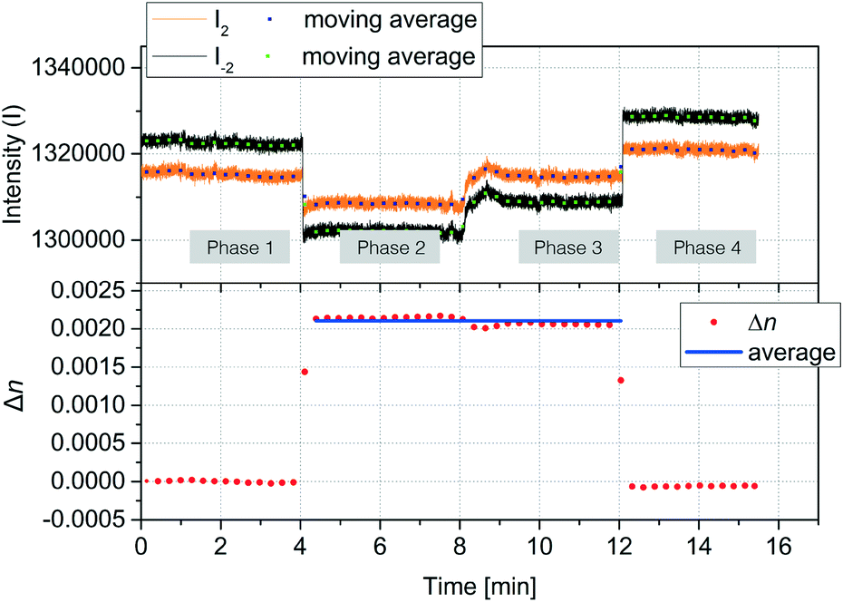 | ||
| Fig. 5 Experimental verification of common mode rejection. Phase 1: DI water in reference and detection channel, T = 25 °C. Phase 2: 2% glycerol solution in detection channel, T = 25 °C. Phase 3: 2% glycerol solution in detection channel, T = 33 °C. Phase 4: DI water in reference and detection channel, T = 33 °C (device dimensions w = 4 μm, l = 6 μm, P = 18 μm). | ||
2.3 Protein detection
To test whether the nanofluidic grating sensor can be used to detect changes in refractive index due to surface binding, we immobilized avidin to the channel walls (Fig. 6). Prior to the experiment all channels had been activated by flowing Piranha solution (1![[thin space (1/6-em)]](https://www.rsc.org/images/entities/char_2009.gif) :3 H2O2:H2SO4) through the system, leaving the channel walls with a thin surface oxide layer. Avidin forms positive clusters that readily attach to the negatively charged oxide layer through electrostatic interactions.54
:3 H2O2:H2SO4) through the system, leaving the channel walls with a thin surface oxide layer. Avidin forms positive clusters that readily attach to the negatively charged oxide layer through electrostatic interactions.54
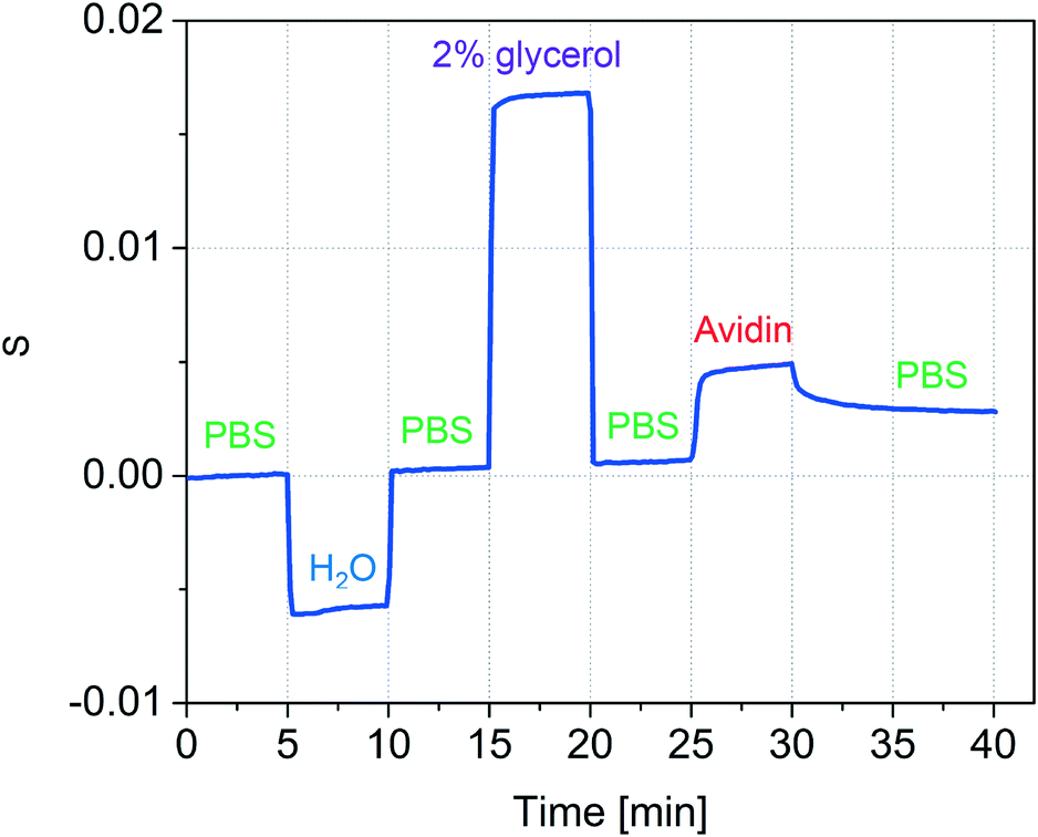 | ||
| Fig. 6 Signal changes (S1) due to sequential sample measurement (water and 2% glycerol) in addition to measurement of protein accumulation of avidin in detection channels (device dimensions w = 4 μm, l = 6 μm, P = 18 μm). | ||
Phosphate buffered saline (1× PBS) was used as the reference and wash solution. After 5 minutes of acquiring a baseline, the solution in the detection channel was exchanged to water in order to verify that the system was correctly responding to bulk solution changes. After another 5 minutes, PBS was again flowed through all channels and the baseline signal was recovered. To confirm the ability of the device to sequentially measure changes in refractive index of multiple solutions, 2% glycerol was then introduced. As expected, the signal increased. Next, PBS was again introduced to all channels and the baseline signal was recovered.
Avidin adsorption was measured by flowing a solution of avidin in PBS (0.5 mg mL−1 avidin in PBS) through the detection channel for 5 minutes and subsequently rinsing with PBS for 10 minutes to remove any loosely bound protein. It is important to note that after the 10 minute rinse, the baseline signal was not recovered, suggesting the avidin molecules adhered tightly to the channel wall. We expect that significantly lower concentrations of protein can be measured provided that the accumulation time is extended or the flow rate is increased.
We expect that our nanofluidic grating sensor could be functionalized with different affinity reagents for the label-free detection of specific biomolecules. For sensitive detection, the large surface-to-volume ratio of these channels should provide distinct advantages, as molecules would have a high capture probability on their passage through the channel. At the same time, the large number of parallel nanochannels provides a large effective capture area, so that rare molecules could be efficiently concentrated in the sensing area.
3 Conclusions
Here we report the development of a new nanofluidic device for simple and robust differential refractive index measurements in an ultra-low volume. Optical differencing is performed directly by an interferometer with a common path for the sensing and the reference arm. This is enabled by guiding the sample and reference fluids through two sets of parallel nanochannels arranged to form an interdigitated optical reflection grating. A key innovation in our design is the asymmetric arrangement of the unit cell of the grating, which shifts the operating point of the interferometer to allow sensitive measurements even when the refractive index of the two solutions is nearly matched.The differential design of our system allows measurements that are inherently compensated for common mode variations. Here, we have shown that common mode refractive index changes due to temperature fluctuations can be suppressed by at least a factor of 10 in the differential signal. The noise floor of the device in our current setup is limited by low-frequency fluctuations to 1.3 × 10⁻⁵ RIU (standard deviation over 4 minutes). Although the sensitivity achieved with our method is currently lower compared to other methods employing microfluidic devices, we expect that this can be significantly improved through both optimization of channel alignment and external measurement components. Moreover, our optofluidic method is superior regarding simplicity and robustness to disturbances.
The separate fluidic addressing of reference and detection channels allows a specific immobilization of molecules in just the detection channels. The capability of quantifying thin adsorbed protein layers in combination with the above described common mode rejection provides the potential for detecting biomolecules label-free with a uniquely simple, robust, and inherently differential sensor. Future applications as a point-of-care device are therefore very attractive.
Conflicts of interest
There are no conflicts of interest to declare.Acknowledgements
This project is funded within the program “Zentrales Innovationsprogramm Mittelstand” by the Bundesministerium für Wirtschaft und Energie (BMWi) (KF3259501MD3/KF3085602MD3). Further funding was provided by a Max Planck Research Group award (T. P. Burg) and by the Max Planck Institute for Biophysical Chemistry. Also, RDL was supported on funding from the European Union's Seventh Framework Programme for research, technological development and demonstration under grant agreement no 331737. Open Access funding provided by the Max Planck Society.References
- S. G. Patching, Biochim. Biophys. Acta, Biomembr., 2014, 1838, 43–55 CrossRef CAS PubMed.
- Q. G. Shi, L. N. Ying, L. Wang, B. J. Peng and C. F. Ying, Appl. Mech. Mater., 2014, 551, 347–352 CrossRef.
- K. S. Rangappa, Proc. Indian Acad. Sci., Sect. B, 1948, 131–143 CAS.
- T. M. Libish, J. Linesh, M. C. Bobby, P. Biswas, S. Bandyopadhyay, K. Dasgupta and P. Radhakrishnan, Optoelectron. Adv. Mater., Rapid Commun., 2011, 5, 68–72 CAS.
- S. Agarwal, Y. Prajapati and V. Mishra, Opto-Electron. Rev., 2015, 23, 271–277 Search PubMed.
- J. Homola, Chem. Rev., 2008, 108, 462–493 CrossRef CAS PubMed.
- F. B. Myers and L. P. Lee, Lab Chip, 2008, 8, 2015 RSC.
- M. Svedendahl, R. Verre and M. Käll, Light: Sci. Appl., 2014, 3, e220 CrossRef CAS.
- F. De-Jun, L. Guan-Xiu, L. Xi-Lu, J. Ming-Shun and S. Qing-Mei, Appl. Opt., 2014, 53, 2007 CrossRef PubMed.
- S. Filion-Côté, M. Tabrizian and A. G. Kirk, Sens. Actuators, B, 2017, 245, 747–752 CrossRef.
- G. G. Yaralioglu, A. Atalar, S. R. Manalis and C. F. Quate, J. Appl. Phys., 1998, 83, 7405–7415 CrossRef CAS.
- C. A. Savran, T. P. Burg, J. Fritz and S. R. Manalis, Appl. Phys. Lett., 2003, 83, 1659–1661 CrossRef CAS.
- K. Hosokawa, K. Hanada and R. Maeda, J. Micromech. Microeng., 2002, 12, 1–6 CrossRef CAS.
- T. Thundat, E. Finot, Z. Hu, R. H. Ritchie, G. Wu and A. Majumdar, Appl. Phys. Lett., 2000, 77, 4061–4063 CrossRef CAS.
- G. Ye and X. Wang, Biosens. Bioelectron., 2010, 26, 772–777 CrossRef CAS PubMed.
- C. L. Chang, Z. Ding, V. N. L. R. Patchigolla, B. Ziaie and C. A. Savran, IEEE Sens. J., 2012, 12, 2374–2379 CrossRef CAS.
- O. J. Schueller, D. C. Duffy, J. A. Rogers, S. T. Brittain and G. M. Whitesides, Sens. Actuators, A, 1999, 78, 149–159 CrossRef CAS.
- Y. G. Tsay, C. I. Lin, J. Lee, E. K. Gustafson, R. Appelqvist, P. Magginetti, R. Norton, N. Teng and D. Charlton, Clin. Chem., 1991, 37, 1502–1505 CAS.
- C.-L. Chang, G. Acharya and C. A. Savran, Appl. Phys. Lett., 2007, 90, 233901 CrossRef.
- C. Lv, Z. Jia, Y. Liu, J. Mo, P. Li and X. Lv, J. Appl. Phys., 2016, 119, 094502 CrossRef.
- P. M. St. John, R. Davis, N. Cady, J. Czajka, C. A. Batt and H. G. Craighead, Anal. Chem., 1998, 70, 1108–1111 CrossRef.
- M. M. Varma, D. D. Nolte, H. D. Inerowicz and F. E. Regnier, Opt. Lett., 2004, 29, 950–952 CrossRef CAS PubMed.
- J. B. Goh, R. W. Loo and M. C. Goh, Sens. Actuators, B, 2005, 106, 243–248 CrossRef CAS.
- BV Metrohm Autolab, Autolab ESPRIT Data Acquisition 4.4 User manual SPR, 2009 Search PubMed.
- Handbook of Spectroscopy, ed. G. Ganglitz and D. S. Moore, Wiley-VCH Verlag GmbH, 2014, p. 1993 Search PubMed.
- A. Ymeti, J. S. Kanger, R. Wijn, P. V. Lambeck and J. Greve, Sens. Actuators, B, 2002, 83, 1–7 CrossRef CAS.
- K. Chaitavon, S. Sumriddetchkajorn and J. Nukeaw, RSC Adv., 2013, 3, 6981 RSC.
- K. Chaitavon, S. Sumriddetchkajorn and J. Nukeaw, RSC Adv., 2013, 3, 23470 RSC.
- A. Ymeti, J. Kanger, J. Greve, P. Lambeck, R. Wijn and R. Heideman, TRANSDUCERS ’03. 12th International Conference on Solid-State Sensors, Actuators and Microsystems. Digest of Technical Papers (Cat. No.03TH8664), 2003, pp. 1192–1196 Search PubMed.
- Z. Wang and D. J. Bornhop, Anal. Chem., 2005, 77, 7872–7877 CrossRef CAS PubMed.
- V. Zamora, P. Lützow, M. Weiland and D. Pergande, Sensors, 2013, 13, 14601–14610 CrossRef PubMed.
- H. Li and X. Fan, Appl. Phys. Lett., 2010, 97, 011105 CrossRef.
- C. F. Carlborg, K. B. Gylfason, A. Kaźmierczak, F. Dortu, M. J. Bañuls Polo, A. Maquieira Catala, G. M. Kresbach, H. Sohlström, T. Moh, L. Vivien, J. Popplewell, G. Ronan, C. A. Barrios, G. Stemme and W. van der Wijngaart, Lab Chip, 2010, 10, 281–290 RSC.
- M. Li, X. Wu, L. Liu, X. Fan and L. Xu, Anal. Chem., 2013, 85, 9328–9332 CrossRef CAS PubMed.
- A. P. Zhang, G. Yan, S. Gao, S. He, B. Kim, J. Im and Y. Chung, Appl. Phys. Lett., 2011, 98, 221109 CrossRef.
- W. Liang, Y. Huang, Y. Xu, R. K. Lee and A. Yariv, Appl. Phys. Lett., 2005, 86, 151122 CrossRef.
- R. St-Gelais, J. Masson and Y.-A. Peter, Appl. Phys. Lett., 2009, 94, 243905 CrossRef.
- T. Wei, Y. Han, Y. Li, H.-l. Tsai and H. Xiao, Opt. Express, 2008, 16, 5764 CrossRef CAS PubMed.
- H. Wu, H. Huang, M. Bai, P. Liu, M. Chao, J. Hu, J. Hao and T. Cao, Opt. Express, 2014, 22, 31977 CrossRef CAS PubMed.
- J. Tian, Y. Lu, Q. Zhang and M. Han, Opt. Express, 2013, 21, 6633 CrossRef CAS PubMed.
- P. Domachuk, I. C. M. Littler, M. Cronin-Golomb and B. J. Eggleton, Appl. Phys. Lett., 2006, 88, 093513 CrossRef.
- S. Surdo, S. Merlo, F. Carpignano, L. M. Strambini, C. Trono, A. Giannetti, F. Baldini and G. Barillaro, Lab Chip, 2012, 12, 4403 RSC.
- S. Surdo, F. Carpignano, L. M. Strambini, S. Merlo and G. Barillaro, RSC Adv., 2014, 4, 51935–51941 RSC.
- S. Mandal and D. Erickson, Opt. Express, 2008, 16, 1623 CrossRef PubMed.
- Z. Xu, X. Wang, K. Han, S. Li and G. L. Liu, J. Opt. Soc. Am. A, 2013, 30, 2466 CrossRef PubMed.
- Z. Xu, K. Han, I. Khan, X. Wang and G. L. Liu, Opt. Lett., 2014, 39, 6082 CrossRef PubMed.
- N. Kumawat, P. Pal and M. Varma, Sci. Rep., 2015, 5, 16687 CrossRef CAS PubMed.
- A. Marin, M. Joanicot and P. Tabeling, Sens. Actuators, B, 2010, 148, 330–336 CrossRef CAS.
- S. Y. Yoon and S. Yang, Lab Chip, 2011, 11, 851 RSC.
- K. Q. Kieu and M. Mansuripur, IEEE Photonics Technol. Lett., 2006, 18, 2239–2241 CrossRef.
- F. Pedrotti, L. Pedrotti, W. Bausch and H. Schmidt, Optik für Ingenieure, Springer Verlag, Berlin, 3rd edn, 2005 Search PubMed.
- K. Takamura, H. Fischer and N. R. Morrow, J. Pet. Sci. Eng., 2012, 98-99, 50–60 CrossRef CAS.
- A. N. Bashkatov and E. A. Genina, Proc. SPIE 5068, Saratov Fall Meeting 2002: Optical Technologies in Biophysics and Medicine IV, (October 14, 2003), 2003, vol. 393, pp. 393–395 Search PubMed.
- Handbook of Single-Molecule Biophysics, ed. P. Hinterdorfer and A. van Oijen, Springer Verlag, 2009, p. 410 Search PubMed.
Footnote |
| † Electronic supplementary information (ESI) available. See DOI: 10.1039/c7lc00929a |
| This journal is © The Royal Society of Chemistry 2017 |