
 Open Access Article
 This Open Access Article is licensed under a
 Creative Commons Attribution 3.0 Unported Licence
On-chip enzymatic microbiofuel cell-powered integrated circuits†
Andrew G.
Mark‡
 a,
Emmanuel
Suraniti‡
a,
Jérôme
Roche§
a,
Harald
Richter
b,
Alexander
Kuhn
cd,
Nicolas
Mano
*ed and
Peer
Fischer
*af
a,
Emmanuel
Suraniti‡
a,
Jérôme
Roche§
a,
Harald
Richter
b,
Alexander
Kuhn
cd,
Nicolas
Mano
*ed and
Peer
Fischer
*af
aMax-Planck-Institut für Intelligente Systeme, Heisenbergstraβe 3, 70569 Stuttgart, Germany. E-mail: fischer@is.mpg.de
bInstitut für Mikroelektronik Stuttgart, Allmandring 30a, 70569 Stuttgart, Germany
cBordeaux INP-UMR 5255, CNRS-ENSCBP, 16 avenue Pey-Berland, 33600 Pessac, France
dUniversité de Bordeaux, 146 rue Léo Saignat, 33076 Bordeaux Cedex, France
eCNRS, CRPP, UPR 8641, 115 Avenue du Docteur Schweitzer, 33600 Pessac, France. E-mail: mano@crpp-bordeaux.cnrs.fr
fInstitut für Physikalische Chemie, Universität Stuttgart, Pfaffenwaldring 55, 70569 Stuttgart, Germany
First published on 26th April 2017
Abstract
A variety of diagnostic and therapeutic medical technologies rely on long term implantation of an electronic device to monitor or regulate a patient's condition. One proposed approach to powering these devices is to use a biofuel cell to convert the chemical energy from blood nutrients into electrical current to supply the electronics. We present here an enzymatic microbiofuel cell whose electrodes are directly integrated into a digital electronic circuit. Glucose oxidizing and oxygen reducing enzymes are immobilized on microelectrodes of an application specific integrated circuit (ASIC) using redox hydrogels to produce an enzymatic biofuel cell, capable of harvesting electrical power from just a single droplet of 5 mM glucose solution. Optimisation of the fuel cell voltage and power to match the requirements of the electronics allow self-powered operation of the on-board digital circuitry. This study represents a step towards implantable self-powered electronic devices that gather their energy from physiological fluids.
Introduction
The lack of a sustainable power source that can harvest energy from the physiological environment is one of the roadblocks to developing electronic biomedical devices for long term implantation. It is counterintuitive that, while physiological fluids teem with energy rich molecules such as fats, adenosine triphosphate and glucose, the energy for contemporary electronic implants is drawn instead from co-implanted man-made batteries of limited capacity. The critical bridging technology is the enzymatic biofuel cell (EBFC) which, by means of enzymes, converts physiologically produced substrates into useful electrical power. Unfortunately, EBFCs currently suffer from drawbacks such as short lifetime, low current densities and limited voltage which often makes them incompatible with the electrical demands of typical implants.1 This is particularly true for miniaturized devices whose small dimensions can only accommodate microbiofuel cells (μBFC) with commensurately reduced current capacity.The key components of an enzymatic biofuel cell are the oxidoreductases immobilized on the two electrodes. Electrons are generated at the anode and consumed at the cathode through enzyme-catalysed electro-oxidation and reduction. The intrinsic properties of enzymes – high catalytic activity at physiological temperature and pH, low overpotential for substrate conversion and absence of reaction side products – are well matched to the requirements for operation in vivo.2 Naturally, the greatest efforts have been focused on the development of BFCs that gather their energy from blood, mostly targeting glucose and dioxygen as substrates due to their availability.3 As a consequence, many EBFCs are based on glucose-oxidizing enzymes like glucose dehydrogenase or glucose oxidase (GOx) and dioxygen-reducing enzymes such as bilirubin oxidase (BOD) or laccase.4 Sustained efforts in EBFC development5 have recently led to enzymatic glucose/O2 BFCs capable of powering biomedical devices in vitro6 and even in vivo.7–9 However, because of their limited power output, these devices still rely on large macroscale electrodes that are decoupled from the devices themselves. EBFC stacking or voltage up-conversion is also usually needed to satisfy the voltage demand of electronics;10–12 this further limits miniaturization and restricts real-world application.
Fortunately, the power characteristics of digital electronics and enzymatic fuel cells have evolved along converging trajectories: the power input demands of electronics have decreased, while the power generating capabilities of EBFCs have increased.13,14 The drastic improvements seen in digital electronics are due, in part, to the practice of very large scale integration (VLSI). Modern devices have been made faster, more reliable, and smaller by integrating billions of transistors implementing diverse functional units into a single piece of silicon. In bio-hybrid systems, closer integration between a digital circuit and its EBFC power source can be expected to yield similar gains and result in systems that are more robust, less expensive, and smaller than existing discrete designs.
In this paper, we present a system which combines an electronic device and the enzymatic micro biofuel cell that powers it, directly into the same silicon chip (see Fig. 1). The power source is a high-performance glucose/O2 enzymatic μBFC and the circuit is a custom application specific integrated circuit (ASIC) implementing a digital counter. The high output potential of the μBFC and the low voltage requirement of the circuit eliminate the need for voltage conversion. This demonstrates a methodology for closer integration between electronic and enzymatic systems which will ultimately lead to improved power systems for electronic implants.
 | ||
| Fig. 1 Simplified schematic of the integrated μBFC (left) and ripple counter (right). Components within the dashed area are integrated on the chip. Current is generated by the enzymatic oxidation of glucose to gluconolactone at the anode, and reduction of dioxygen to water at the cathode. The power supplied drives the counter which is composed of D-flip-flops (F1 to F4) that successively divide the frequency of the input signal DIN at each stage of the output D1 to D4. O1–O4 are on-chip output drivers, B1–B4 are off-chip buffers (AD8244), and J1 and J2 are off-chip removable jumpers that can decouple the source from the load during testing. | ||
One of the major advances towards integrated EBFCs has been the introduction of redox hydrogels to electronically connect the active redox centres of enzymes to the electrode surfaces.15 These allow current densities of ∼mA cm−2 by embedding a high density of enzymes within a permeable 3D-polymer matrix containing mobile redox mediators, usually osmium complexes, tethered to the polymer backbone. This ensures optimal electron transfer to the underlying metal electrode, regardless of enzyme orientation.16 The redox potentials of the osmium moieties can be tuned to optimize electron transfer for each oxidoreductase while maximizing the open circuit potential (OCP, the highest voltage that can be reached, at zero current) of the BFC.17 The substrate specificity of enzymes, tightly bound to their respective electrodes, permits operation without a separation membrane.
μBFCs based on redox hydrogels have demonstrated energy harvesting from physiological fluid, including glucose solutions,18 and recently even human blood.19 The latter have demonstrated high power densities on the order of 100 μW cm−2, thus opening the possibility of implantation.20 In addition, integration of EBFCs has been demonstrated in the context of self-powered sensors,21 and EBFCs have been proposed as power sources for wearable electronics embedded in contact lenses.22,23 Combined with a well-adapted preparation method for μ-electrodes, this can be a facile route towards μBFCs with high power densities, a requirement for direct integration into miniaturized devices with limited surface areas.24
Methods and materials
μBFC integrated logic circuit
Our device integrates two distinct functions, a μBFC power source and a digital counter circuit, into a single die. The device is based on an IMS GFQ100 gate forest library, implemented in 0.5 μm CMOS (IMS Chips, Stuttgart, Germany) on a 4.6 mm square die. The chip uses a semi-custom design methodology to realize arbitrary circuit function within an ASIC. As seen in Fig. 1, for this work we have implemented a generic four-bit ripple counter.Following CMOS processing, the circuit is further functionalized as illustrated in Fig. 2. The top face of the chip die is coated with a silicon nitride barrier layer (Fig. 2b) and two aluminum electrode foundations (0.8 μm × 1.2 mm × 3.6 mm, Al![[thin space (1/6-em)]](https://www.rsc.org/images/entities/char_2009.gif) :Cu:Si 99%:0.5%:0.5%) with connections to the perimeter wire bond pads. The electrode foundations are sputter coated with 500 nm of Au, upon a 5 nm Ti adhesion layer (Fig. 2c). The regions to be coated are defined by a mylar shadow mask aligned to the electrode foundations. The chips are then packaged into a ceramic IC carrier (CLCC84), with electrical connections made by wire bonding to the package (Fig. 2d and h). The bond wires are mechanically protected with UV-polymerizable epoxy (NOA 65; Norland Optical, Cranbury, NJ, USA), followed by a thin layer of silicone (CAF 4; Bluestar Silicones, Lyon, France) to define a watertight macrowell (2.5 mm × 2.5 mm) which partially exposes the two electrode faces (Fig. 2e).
:Cu:Si 99%:0.5%:0.5%) with connections to the perimeter wire bond pads. The electrode foundations are sputter coated with 500 nm of Au, upon a 5 nm Ti adhesion layer (Fig. 2c). The regions to be coated are defined by a mylar shadow mask aligned to the electrode foundations. The chips are then packaged into a ceramic IC carrier (CLCC84), with electrical connections made by wire bonding to the package (Fig. 2d and h). The bond wires are mechanically protected with UV-polymerizable epoxy (NOA 65; Norland Optical, Cranbury, NJ, USA), followed by a thin layer of silicone (CAF 4; Bluestar Silicones, Lyon, France) to define a watertight macrowell (2.5 mm × 2.5 mm) which partially exposes the two electrode faces (Fig. 2e).
 | ||
| Fig. 2 Construction process of the on-chip μBFC. Side (left) and front (right) views. a) Integrated circuit die with CMOS components. b) Deposition of two independent aluminum electrodes (dark grey) and titanium nitrate passivation layer (SiNx, light grey). c) Gold electrodes defined by shadow deposition (orange). d) Wirebond connections between IC and package. e) Encapsulation of wires and remaining aluminum by epoxy and silicone elastomer (green) to create a macrowell. f) Gold microelectrodes defined by nailpolish (pink). g) Enzyme functionalization: GOx (blue) and BOD (yellow) hydrogels. h) Photograph of the wired gold electrodes before encapsulation (step d). i) Photo of gold microelectrodes, visible as small exposed circles on left and right region of chip (step f). | ||
Finally, each microelectrode is defined by drop casting acetone diluted nail lacquer (10:1; Wj-con) around a temporary poly-dimethylsiloxane mask (PDMS; Sylgard 184; Dow Corning Corporation, Midland, MI, USA). The masks consisted of a ∅400 μm cured PDMS cylinder extruded from a 10 μL pipet tip. Each mask is pressed into contact with the gold electrode surface under visual control and subsequently diluted nail lacquer is drop cast around it. After 5 minutes of drying the mask is removed to reveal the exposed gold disk electrode (Fig. 2f and i). Once the two microelectrodes are defined, the surface is rinsed with Milli-Q water. The influence of the distance between the two microelectrodes, which will affect the internal cell resistance, was not explored. However, because the μBFC operating current is extremely low (nA-range) and because the ionic strength of the experimental buffer is very high, ohmic losses in the electrolyte will be correspondingly low, and the microelectrode placement is not expected to be critical. This hybrid fabrication process is well-adapted to rapid development of the proof-of-principle system described here as it permits exploration of parameters such as the electrodes size, which would be time-consuming if undertaken using photolithographic microfabrication processes. However, the important characteristics of the method – a small exposed electrode area surrounded by an insulating polymer layer – can be easily replicated using lithographic techniques for future process streamlining and device miniaturization.
Details of the final step of biofunctionalization (Fig. 2g) are reported below. Testing and setup is simplified by segregating the power and logic functions of the device: connections between them are made through the bond pads at the chip perimeter (and ultimately through the pins on the package). This permits testing of the μBFC performance and logic functions to be performed independently. Currently, connections between the two segments of the chip are made at the package level, but the same processes can implement the connections on-die. This will permit further miniaturization, necessary for integration in a complete implantable device.
Test setup
A multipurpose custom printed circuit board serves as the interface between the chip and the measurement instrumentation. We mainly used it in two configurations: for electrochemical characterization of the microelectrodes, the board was set up to allow direct connection of the bi-potentiostat to each electrode independently. During digital circuit testing, a Keithley 2000 high impedance multimeter (Tektronix, Beaverton, OR, USA) monitored the μBFC working potential while a Keithley 6487 picoammeter (Tektronix) measured its output current. The counter input signal was a 400 mVpp square wave supplied by an Agilent 33220A (Keysight, Santa Rosa, CA, USA) function generator. The output signals from the counter were buffered through a high input impedance AD8244 amplifier (Analog Devices, Norwood, MA, USA) with unity gain, and measured by a Tektronics TDS 2024C multi-channel oscilloscope. Light falling on the device induces photocarriers which lead to an increase in drain current by several orders of magnitude. Therefore, the device testing was always carried out with the chip shrouded by aluminum foil.Electrochemical characterization
All solutions were prepared in Milli-Q water (18.2 MΩ cm), with analytical grade reagents. Electrochemical measurements were performed using a CH Instruments 760C bi-potentiostat (CH Instruments, Austin, TX, USA), with a Ag/AgCl (KCl 3 M) reference electrode (BASi, West Lafayette, IN, USA) and a platinum wire counter electrode. A 1 mm thick PDMS gasket with a 5 × 5 mm2 central well was used to seal a larger (∼2 mL capacity) funnel-shaped glass well to the face of the chip.Characterization of microelectrodes
The cleanliness of the bare gold microelectrodes was confirmed by cyclic voltammetry (CV; −0.225 V to +1.6 V vs. Ag/AgCl at 100 mV s−1) in 0.1 M H2SO4 (99%; Sigma-Aldrich, St. Louis, MO, USA). These CVs show the expected shape of gold oxide stripping with a reduction peak at +0.9 V (Fig. SI1a†). The active gold surface areas of the microelectrodes were estimated from the integrated charge of the peak using a conversion factor of −390 μC cm−2.25 The measurements indicate surface areas of 0.13 ± 0.01 mm2, corresponding to diameters of 410 ± 20 μm. CVs at 2 mV s−1 with 5 mM Ru(NH3)63+(Cl3) (98%; Sigma-Aldrich) in a 0.1 M NaCl buffer (Fig SI1b†) give a complementary measurement of 423 ± 8 μm for the effective diameter of the electrodes.26 The mean of the electrochemical measurements of the electrode diameters, 416 ± 17 μm, is in good agreement with the optical estimate of around 400 μm.Microbiofuel cell preparation
Immediately before functionalization with the hydrogel, the microelectrodes were cleaned and rendered hydrophilic by a series of CVs in sulfuric acid, then rinsed with water and dried for 30 minutes at room temperature. The two active enzymes are glucose oxidase (GOx) from Aspergillus niger, purchased from Sigma and purified as reported earlier,27 and bilirubin oxidase (BOD) from Magnaporthe oryzae produced and purified as described in ref. 28. Enzyme immobilization results from the formation of an electrostatic adduct between the polyanionic enzymes and polycationic redox polymers. The adduct is further strengthened by the addition of a cross linker. The cross linker exhibits at its two ends epoxy groups that can react with functional amino acids present at the surface of enzymes and polymer backbone.24 Redox hydrogel electrodes were prepared as reported earlier for both the anodic29 and cathodic sides.30The anodic hydrogel consists in an aqueous solution of 55 wt% PVP Os[(1,1-dimethyl-2,2'biimidazole)2-2-[6 methylpyrid-2yl] imidazole]2+/3+ with a redox potential of −30 mV vs. Ag/AgCl,29 35 wt% GOx and 10 wt% polyethylene glycol 400 diglycidyl ether (PEGDGE; Polysciences, Inc., Warrington, PA, USA), for a total mass concentration of 5.08 mg mL−1. The cathodic hydrogel is composed of 62.6 wt% PAA-PVI-[Os(4,4′-dichloro-2,2′-bipyridine)2Cl]+/2+ with an apparent redox potential of +350 mV vs. Ag/AgCl, 30 wt% BOD from M. oryzae and 7.4 wt% PEGDGE,30 leading to a 6.26 mg mL−1 solution.
The electrodes were modified with the appropriate hydrogel solution in each microwell (Fig. 2g) in four successive steps of 0.5 μL coatings separated by 10 minutes of drying at room temperature. Dividing the total amount of deposited hydrogel by the active gold surfaces gives respective loadings of 7.46 and 9.21 mg cm−2 at the anode and cathode. Once deposited, the hydrogels were cured for 18 hours at 4 °C, protected from dust, allowed to equilibrate under ambient conditions for 45 minutes, and gently rinsed two times with phosphate buffer before experiments were started.
μBFC characterization
All experiments were performed in an air-conditioned lab with the temperature fixed at 19 °C. CVs at 100 and 5 mV s−1 were first performed in 100 mM phosphate buffer (PB) at pH 7.2 using a typical three electrode configuration in the absence of glucose and in argon-purged buffer for polymer characterization. Electrocatalysis was performed in aerated PB containing 5 mM glucose under quiescent conditions, with neither convection nor oxygen bubbling. Power curves were measured as reported earlier between +0.75 V and 0 V at 5 mV s−1.19Self-powered chip function
The potentiostat was unplugged and the test setup was reconfigured for measuring the chip performance (see section “test setup” above), so that the integrated μBFC powered the logic function of the chip while the power and digital performance were assessed. The μBFC was fuelled by a 50 μL droplet of a 5 mM glucose solution in PB. The droplet was replaced every 2 h to minimize variations in glucose concentration due to evaporation. The binary counting function was allowed to run continuously while every 30 minutes a trace of the binary counting signal was recorded on the oscilloscope, and the current and voltage at the μBFC output were measured with the picoammeter and voltmeter.Results and discussion
Characterization of the digital circuit
The ASIC is a generic 4-bit ripple counter based on D-flip-flops. Briefly, the circuit takes an externally supplied input clock signal, and successively divides the input frequency f by two for each successive output, D1–D4. Taken together, the states of the output channels provide a binary count of the number of clock pulses since the last reset or rollover. The rated supply voltage for this architecture is VDD = 4.5–5.5 V (NMOS/PMOS threshold voltage 0.8 V/0.9 V), at which it can process input clock speeds in excess of 250 MHz. However, because of its low power consumption design, it is able to operate at a reduced clock rate, down to supply voltages as low as 500 mV, well below threshold voltages. Typical power characteristics at VDD = 700 mV and f = 60 Hz is a consumption of ∼560 pW. However, below 700 mV the output signal quality diminishes rapidly (see Fig. SI2†). This low voltage operation, not exploited in general use, decreases the power requirements into the range where enzymatic microbiofuel cells are possible candidates for supplying power, even without voltage boost conversion. The challenge is then to design an on-chip fuel cell with sufficiently high output voltage to power the chip.Optimization and characterization of enzyme electrodes
The critical components of the μBFC are the enzyme microelectrodes, each composed of a redox hydrogel containing the active enzyme and immobilized on the integrated Au microelectrode. The construction of the hydrogel disk microelectrodes was optimized through a series of experiments conducted on gold-coated glass slides which were prepared in the same manner as the integrated chip electrodes. Short circuit current and onset potentials (potential at which the electrocatalysis starts) under μBFC working conditions were studied as a function of the volume of deposited hydrogel for anode and cathode (Fig. SI3†). For both electrodes, bell-shaped curves as a function of the loading are obtained, as expected in conditions of low substrate concentration and quiescent conditions.31,32 An increase in hydrogel thickness limits the mass-transport, slows down the electron diffusion towards the electrodes and therefore decreases the current density (Fig. SI3b†).However, at the same time, as illustrated for example in Fig SI3c† for the cathode, increasing the hydrogel thickness permits an increase in the onset potential for O2 reduction which will ultimately increase the OCP of the BFC. Since the OCP is the crucial parameter in our system, high hydrogel loadings were preferred.
Integrated μBFC characterization
Once cleaned and characterized, the bare Au on-chip electrodes were functionalized with the optimized hydrogel loading evaluated above. A series of CVs (100 mV s−1, Fig. 3a) were recorded in argon-purged buffer solution without substrates, to verify the presence and stability of the hydrogel layer. They show well-defined and stable oxidation and reduction peaks at both anode and cathode, with mean potentials of −27 mV (anode, blue) and +335 mV (cathode, green) vs. Ag/AgCl, in agreement with the redox potential of each polymer. The oxidation-to-reduction peak separations are in the order of 90 mV (73 mV at the anode and 106 mV at the cathode) and indicate good reversibility in both hydrogels. The biocatalytic performance of the microelectrodes were characterized at low scan rate (5 mV s−1) in an aerated PB at 19 °C after the addition of 5 mM glucose, in the absence of O2 bubbling or convection. | ||
| Fig. 3 Electrochemical characterization of the on-chip microbiofuel cell. a) Under Ar, in the absence of substrate and at 100 mV s−1. b) Catalytic currents at the anode (blue) and cathode (green) in the presence of 5 mM aerated glucose solution, 19 °C, and no forced convection. c) Polarization curve (black) and the corresponding power curve (red). CVs at 5 mV s−1vs. Ag/AgCl (b) or vs. anode (c) as a reference, in aerated PB. | ||
As seen in Fig. 3b, well-defined catalysis could be observed at both the anodic (blue) and cathodic (green) sides of the μBFC on which oxidation of glucose and reduction of dioxygen take place respectively. The CVs exhibit a typical shape for mass-transport limited systems, with maximal catalytic currents of 116 nA (85 ± 7 μA cm−2) at the anode and −166 nA (122 ± 10 μA cm−2) at the cathode. The dominant contribution to the uncertainties in current density comes from the electrochemically measured microelectrode diameter. Finally, the performance of the microelectrodes working together as a complete μBFC power supply was determined and the resulting polarization curve is shown in Fig. 3c (black curve). The maximum current produced by the μBFC is 116 nA and is limited by the anodic side as expected from the independent current measurement (Fig. 3b). The corresponding power curve (Fig. 3c, red curve) exhibits a maximum of 39 nW (29 ± 2 μW cm−2) at a potential of +0.357 V, with an OCP of 0.725 V. When done with a single deposition step of 0.6 μL of hydrogel, the on-chip μBFC exhibits almost the same maximal power (36 nW) but with an OCP of only 0.63 V, which demonstrates the importance of our 4 step deposition protocol.
Self-powered logic operation
In the following we demonstrate the fully integrated self-powered operation of the device. The chip was configured as shown in Fig. 1 so that all power for the chip function was supplied by the μBFC. Upon fuelling with a 50 μL droplet of aerated 5 mM glucose solution the binary counter operation was immediately observed.After 20 minutes of operation, consumption was 1.17 nA at 672 mV at an input clock rate of 50 Hz. This is in good agreement with the corresponding measurement of 1.3 nA from the polarization curve at this potential. Fig. 4a depicts the binary output signals from all four stages of the counter after 45 minutes of operation. Each channel shows the expected division of waveform, with sharp transitions between the on–off states, and a high-state voltage of approximately 0.66 V, in good agreement with VDD = 0.659 V. The 50 Hz ripple superimposed on the high-state arises from radiated mains power interference. At 100 Hz (Fig. 4b) the output performance remains almost identical, but the current consumption increases from 1.22 to 1.33 nA and the supply voltage drops to 0.655 V. However, operation at 200 Hz (Fig. 4c) leads to strong degradation of the D1 channel signal because the on-chip output driver is too slow for operation under these conditions. The internal logic is still functioning as expected as shown by the correct waveforms from the downstream channels D2 to D4.
 | ||
| Fig. 4 Frequency performance under power of the integrated μBFC showing output of channels D1–D4 of the digital counter. a) Input 50 Hz (1.22 nA, 0.659 V). b) 100 Hz (1.33 nA, 0.655 V). c) 200 Hz (1.71 nA, 0.646 V). Acquired after 45 minutes of continuous operation in a 50 μl droplet of 5 mM glucose. Input signal 400 mVpp. | ||
Long term experiments were performed to assess system longevity. Output waveforms were collected every half hour, and the glucose solution was replaced every 2 hours to limit changes in glucose concentration due to evaporation. Considering a typical current of 1 nA, less than 40 pmol of glucose were consumed in 2 hours, which represents a negligible fraction of the 250 nmol contained in the droplet. After 8 h of continuous operation there was very little degradation in the output signal quality.
Fig. 5a compares the D4 output waveform at the start of the experiment (dark blue) and after almost 7.5 h of continuous operation (light blue). The later waveform shows an increase in rise time due to the exponential dependence of the PMOS transistor current on the supply voltage and a small decrease in amplitude.
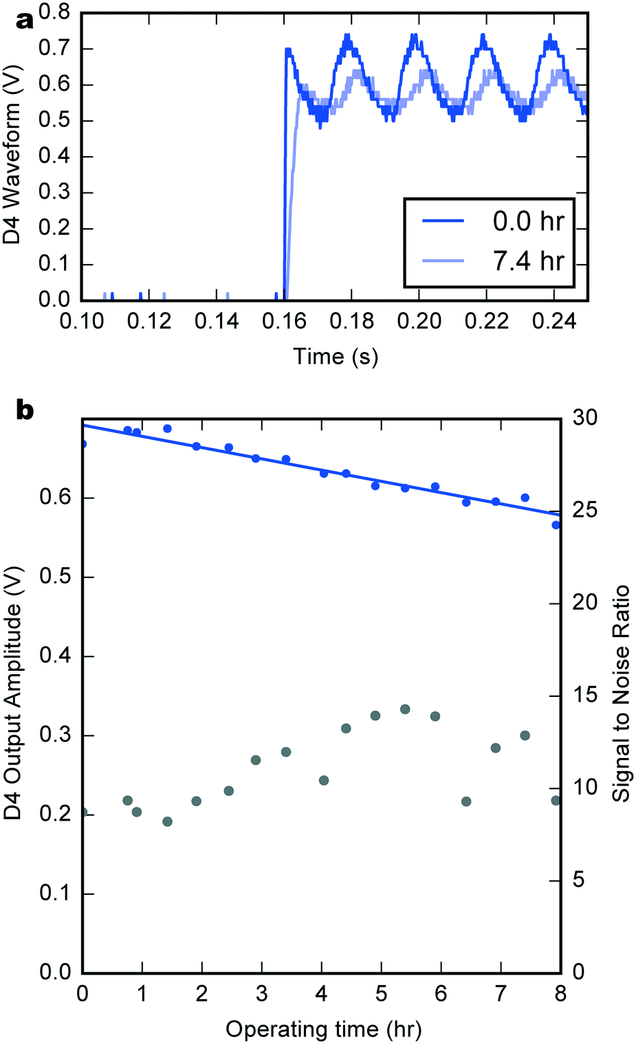 | ||
| Fig. 5 Long term counting performance under integrated biofuel cell power. a) Output waveform of the D4 channel after 0 (dark blue) and 7.4 h (light blue) of continuous device operation in one droplet. b) The output amplitude of the D4 signal (magenta) over 8 h of continuous operation. The amplitude decreases concomitantly with the BFC output potential. The signal to noise ratio (grey) remains roughly constant. | ||
Fig. 5b shows the trend of the waveform amplitude (extracted using a fitting process) during the experiment (see also Fig. SI4† for other channels). The lower curve is the signal to noise ratio (noise being defined as the mean squared deviation between the square-wave fit and the measured signal) which remains approximately constant throughout. The signal amplitude decreases by 14.2 mV h−1, consistent with the trend exhibited by the supply voltage. Taking a minimum usable output amplitude of 0.5 V, this gives a total device lifetime of roughly 14 h. Again, the sequential deposition of hydrogels extended the system's lifetime, as demonstrated by the counting signal at 7.5 h of operation (576 mV, 2.1 nA) which is almost superimposable with the one after only 2 h 30 min for a one-step deposition BFC (573 mV, 0.3 nA).
The degradation of the signal over time is due to the stability of the μBFC. Post-experiment power curves indeed showed a decrease in open circuit potential of 80 mV and a 90% drop in peak power after 25 hours of continuous operation (Fig. SI5a†). The anode was more affected by the long operation than the cathode, as it exhibited a 90% loss in catalytic current while the cathode diminished by only 50%. Although the loss in current is usually due to enzyme instability, in this case degradation of the hydrogel also contributes. This is evidenced by the shift in potential that was observed at both the anode and cathode (Fig. SI5b†) and also by the increase in lifetime with the number of deposition steps.
Conclusions
In this contribution, we report the first example of an application specific integrated circuit that embeds a dedicated enzymatic microbiofuel cell to supply its power. The low power consumption (nW) and low input voltage (sub-V) requirements of the circuit enable it to perform its logic operation under continuous self-power for 14 hours. Over the course of the run it consumed less than 0.3 nmol of glucose from a single drop of quiescent solution at typical blood-glucose concentrations.Clear improvements can be achieved by increasing the drive strength of the output stages (O1–O4) to eliminate the off-chip buffers B1–B4. Also, the ultimate goal of all-foundry processing can be achieved in a MEMS add-on processing line. This would allow lithographic definition of the Au microelectrodes, and the use of a polyimide encapsulation. Finally, the deposition of hydrogel in well-defined geometries can be improved by adopting inkjet techniques. These improvements can all be expected to increase device robustness and decrease device size.
Further miniaturization of the system does not represent any conceptual difficulties and thus allows envisioning integration as the data processing part of a real biomedical implant. For example, the current circuit has a footprint of only 322 × 22 μm2 – the vast majority of the silicon die is unused – this means that, in principle, the electrodes are what limits downscaling. Reducing the chip size to match the extent of the electrodes, here ∅400 μm, would make the device small enough to fit within a 22 gauge hypodermic needle. This would permit implantation within a blood vessel or between the brain's pia matter and arachnoid. Both blood and cerebrospinal fluid are glucose-rich physiological fluids.4 For our device such extreme downscaling would face difficulties in die singulation, hydrogel application and alignment, and device handling. But conventional batteries would be difficult to adapt to such applications because miniaturizing them is complicated by the need for a case, separating membrane and other components.3,24
The efficiency of electrodes of similar composition in human blood samples has already been demonstrated and the improvement of their operational stability is in progress.19 The higher temperatures experienced by an implanted device in vivo are expected to improve system performance by increasing the available μBFC current while simultaneously reducing the circuit's threshold voltage. Longevity remains the most important concern; apart from engineering more stable enzymes,33 mechanical strengthening of the hydrogel, principally by increasing the cross-linking, is one option to increase its lifetime. The other approach is to cover the electrodes with a permeable biocompatible polymer.34 This might sufficiently enhance the operational stability of such self-powered ASICs to the point that they can be used as implantable biomedical devices.
The binary counter presented here stands as a proxy for more complex functions that can be implemented with the same low-voltage CMOS circuitry. However, even simple counters are useful for recording data from sensors whose output can be used as the clock signal. Examples include temperature or capacitance transducers based on ring oscillators whose output is encoded in the frequency of a binary signal akin to the clock signal used here. In fact, these types of sensors could even be fabricated alongside the counter itself in the same silicon die, and with minimal additional circuitry or power requirements. Increasing the storage capacity of the counter results in only small increases in energy consumption since the activity of each added stage is only half of its predecessor. RF-ID is a natural candidate for device readout since it is non-contact and self powered. The two power sources complement one another: the μBFC supplies low power for sensing and recording over many weeks or months, and the RF-ID link supplies the intermittent high power necessary during data downlink. Our system could then fulfill Heller's vision of microbiofuel cells powering “miniature autonomous sensor-transmitter packages which would broadcast for a few weeks the local temperature of a site, indicative of local inflammation”.24
Acknowledgements
The authors thank la Région Aquitaine, the ANR RATIOCELLS (12-BS08-0011-01) and the European project BIOENERGY (FP7-PEOPLE-2013-ITN607793) for financial support. E. S. is grateful for having received a Max-Planck Society scholarship. Open Access funding provided by the Max Planck Society.References
- D. Leech, P. Kavanagh and W. Schuhmann, Electrochim. Acta, 2012, 84, 223–234 CrossRef CAS.
- S. C. Barton, J. Gallaway and P. Atanassov, Chem. Rev., 2004, 104, 4867–4886 CrossRef CAS PubMed.
- M. Falk, C. W. Narváez-Villarubia, S. Babanova, P. Atanassov and S. Shleev, ChemPhysChem, 2013, 14, 2045–2048 CrossRef CAS PubMed.
- S. Cosnier, A. Le Goff and M. Holzinger, Electrochem. Commun., 2014, 38, 19–23 CrossRef CAS.
- M. Rasmussen, S. Abdellaoui and S. D. Minteer, Biosens. Bioelectron., 2016, 76, 91–102 CrossRef CAS PubMed.
- M. Southcott, K. MacVittie, J. Halámek, L. Halámkova, W. D. Jemison, R. Lobel and E. Katz, Phys. Chem. Chem. Phys., 2013, 15, 6278–6283 RSC.
- A. Zebda, S. Cosnier, J. P. Alcaraz, M. Holzinger, A. Le Goff, C. Gondran, F. Boucher, F. Giroud, K. Gorgy, H. Lamraoui and P. Cinquin, Sci. Rep., 2013, 3, 1516, DOI:10.1038/ srep01516.
- K. MacVittie, J. Halámek, L. Halámkova, M. Southcott, W. D. Jemison, R. Lobel and E. Katz, Energy Environ. Sci., 2013, 6, 81–86 CAS.
- A. Szczupak, J. Halámek, L. Halámkova, V. Bocharova, L. Alfonta and E. Katz, Energy Environ. Sci., 2012, 5, 8891–8895 CAS.
- P. Nadeau, D. El-Damak, D. Glettig, Y. L. Kong, S. Mo, C. Cleveland, L. Booth, N. Roxhed, R. Langer, A. P. Chandrakasan and G. Traverso, Nat. Biomed. Eng., 2017, 1, 0022 CrossRef.
- M. Falk, M. Alcalde, P. N. Bartlett, A. L. De Lacey, L. Gorton, C. Gutierrez-Sanchez, R. Haddad, J. Kilburn, D. Leech, R. Ludwig, E. Magner, D. M. Mate, P. Ó. Conghaile, R. Ortiz, M. Pita, S. Pöller, T. Ruzgas, U. Salaj-Kosla, W. Schuhmann, F. Sebelius, M. Shao, L. Stoica, C. Sygmund, J. Tilly, M. D. Toscano, J. Vivekananthan, E. Wright and S. Shleev, PLoS One, 2014, 9(10), e109104 Search PubMed.
- E. Katz and K. MacVittie, Energy Environ. Sci., 2013, 6, 2791–2803 CAS.
- B. I. Rapoport and R. Sarpeshkar, PLoS One, 2012, 7(6), e38436 CAS.
- S. Shleev, A. Bergel and L. Gorton, Bioelectrochemistry, 2015, 106, 1–2 CrossRef CAS PubMed.
- A. Heller, Acc. Chem. Res., 1990, 23, 128–134 CrossRef CAS.
- A. Heller, J. Phys. Chem. B, 1992, 96, 3579–3587 CrossRef CAS.
- A. Heller, Curr. Opin. Chem. Biol., 2006, 10, 664–672 CrossRef CAS PubMed.
- F. Gao, L. Viry, M. Maugey, P. Poulin and N. Mano, Nat. Commun., 2010, 1, 2, DOI:10.1038/ncomms1000.
- M. Cadet, S. Gounel, C. Stines-Chaumeil, X. Brilland, J. Rouhana, F. Louerat and N. Mano, Biosens. Bioelectron., 2016, 83, 60–67 CrossRef CAS PubMed.
- N. Mano, F. Mao and A. Heller, J. Am. Chem. Soc., 2003, 125, 6588–6594 CrossRef CAS PubMed.
- M. Zhou, Electroanalysis, 2015, 27, 1786–1810 CrossRef CAS.
- R. C. Reid, S. D. Minteer and B. K. Gale, Biosens. Bioelectron., 2015, 68, 142–148 CrossRef CAS PubMed.
- M. Falk, V. Andoralov, M. Silow, M. D. Toscano and S. Shleev, Anal. Chem., 2013, 85, 6342–6348 CrossRef CAS PubMed.
- A. Heller, Phys. Chem. Chem. Phys., 2004, 6, 209–216 RSC.
- S. Trasatti and O. A. Petrii, Electroanal. Chem., 1992, 321, 353–376 CrossRef.
- A. J. Bard, J. A. Crayston, G. P. Kittlesen, T. Varco Shea and M. S. Wrighton, Anal. Chem., 1986, 58, 2321–2331 CrossRef CAS.
- F. Gao, O. Courjean and N. Mano, Biosens. Bioelectron., 2009, 25, 356–361 CrossRef CAS PubMed.
- F. Durand, S. Gounel, C. H. Kjaergaard, E. I. Solomon and N. Mano, Appl. Microbiol. Biotechnol., 2012, 96, 1489–1498 CrossRef CAS PubMed.
- E. Tremey, E. Suraniti, O. Courjean, S. Gounel, C. Stines-Chaumeil, F. Louerat et and N. Mano, Chem. Commun., 2014, 50, 5912–5914 RSC.
- M. Cadet, X. Brilland, S. Gounel, F. Louerat and N. Mano, ChemPhysChem, 2013, 14, 2097–2100 CrossRef CAS PubMed.
- T. J. Ohara, R. Rajagopalan and A. Heller, Anal. Chem., 1993, 65, 3512–3517 CrossRef CAS PubMed.
- C. Taylor, G. Kenausis, I. Katakis and A. Heller, J. Electroanal. Chem., 1995, 396, 511–515 CrossRef.
- S. Rubenwolf, S. Kerzenmacher, R. Zengerle and F. Von Stetten, Appl. Microbiol. Biotechnol., 2011, 89, 1315–1322 CrossRef CAS PubMed.
- D. Jain, A. Karajic, M. Murawska, B. Goudeau, S. Bichon, S. Gounel, N. Mano, A. Kuhn and P. Barthélémy, ACS Appl. Mater. Interfaces, 2017, 9, 1093–1098 CAS.
Footnotes |
| † Electronic supplementary information (ESI) available. See DOI: 10.1039/c7lc00178a |
| ‡ These authors contributed equally to this work. |
| § Present address: CIRIMAT, Université de Toulouse, UPS-INP-CNRS, 118 Route de Narbonne, 31062 Toulouse Cedex 09, France. |
| This journal is © The Royal Society of Chemistry 2017 |