 Open Access Article
 This Open Access Article is licensed under a
 Creative Commons Attribution 3.0 Unported Licence
Plasmonic response and SERS modulation in electrochemical applied potentials
G.
Di Martino
 *a,
V. A.
Turek
a,
C.
Tserkezis
b,
A.
Lombardi
a,
A.
Kuhn
c and
J. J.
Baumberg
*a
*a,
V. A.
Turek
a,
C.
Tserkezis
b,
A.
Lombardi
a,
A.
Kuhn
c and
J. J.
Baumberg
*a
aNanoPhotonics Centre, Cavendish Laboratory, University of Cambridge, CB3 0HE, UK. E-mail: gd392@cam.ac.uk; jjb12@cam.ac.uk
bDepartment of Photonics Engineering, Technical University of Denmark, Ørsteds Plads 343, DK-2800 Kgs. Lyngby, Denmark
cUniv. Bordeaux, CNRS 5255, Bordeaux INP, Site ENSCBP, 33607, Pessac, France
First published on 27th April 2017
Abstract
We study the optical response of individual nm-wide plasmonic nanocavities using a nanoparticle-on-mirror design utilised as an electrode in an electrochemical cell. In this geometry Au nanoparticles are separated from a bulk Au film by an ultrathin molecular spacer, giving intense and stable Raman amplification of 100 molecules. Modulation of the plasmonic spectra and the SERS response is observed with an applied voltage under a variety of electrolytes. Different scenarios are discussed to untangle the various mechanisms that can be involved in the electronic interaction between NPs and electrode surfaces.
Understanding the dynamics of charge transport across nanostructures is a key challenge in the creation of ultrathin functional devices. Electrochemistry plays a strong role for such charge transport in many devices, including the new generations of resistive random access memory involving metal/thin-insulator/nanomaterial constructs, as well as in photocatalytic systems, and in surface (bio)chemical sensors. Probes of the mechanisms of surface electrochemistry have mainly utilised frequency-dependent electrical measurements, leaving many questions unanswered such as the location of double layers and the spatial distribution of co/counter-ions in nanostructured materials. We choose here the simple example of a molecule-coated metal electrode, and show how optical spectroscopy using plasmonics and surface-enhanced Raman scattering (SERS) can provide more insight into these challenges.
In the simple system consisting of a metal electrode coated with an organic self-assembled monolayer (SAM), the rate of electron transfer through the SAM has been shown to decay exponentially as the chain length of the monolayer is increased.1 Adsorption of metal nanoparticles (NPs) onto such layers results in an overall charge transfer across the modified electrode.2 Surprisingly, several electrochemical investigations of nanoparticle-mediated electron transfer across the organic layers2–5 show distance-independent charge transfer between two metals when separated by gaps as wide as 6.5 nm.3 Charge transfer across the gaps has proven to be much faster than electron transfer between a metal and the dilute redox species in solution (estimates suggest up to 1012 times faster through an organic layer compared to redox transfer at the metal surface5). In this description, the metal/thin-insulator/metal stack effectively short-circuits when the NPs adsorb,3 making the NPs an extension of the electrode underneath the organic layer.5 In all of this work, the electronic transport between the NP and electrode surfaces has been investigated with impedance measurements. Characterization of the electrodes at the single NP level is thus challenging, with few experimental studies reported.6–9 An improved understanding of this surface chemistry is however crucial for catalysis, as well as a host of photo-electrochemical applications.
Here we utilise the plasmonic response of Au nanoparticle-on-mirror (NPoM) constructs immersed in an electrochemical solution (Fig. 1a) to gather information on the electronic properties of single NPs and molecules near a metallic surface. Upon illumination the NPoM plasmonic system traps light of particular resonant colours in the gap (filled by the SAM) between the NP and the bottom gold electrode. This resonant colour from localised plasmons is actively tuned by the local charge density and surrounding dielectric environment. The optical dark-field scattering spectrum of a NP near a metallic surface consists of several modes. A weaker mode corresponding to transverse dipolar charge oscillations inside the NP alone is seen at 540 nm while a dipole mode resulting from longitudinal coupling between the NP and its image in the mirror surface is seen around 700 nm (Fig. 1b).10
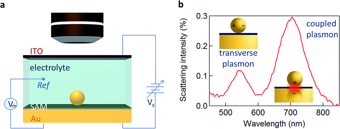 | ||
| Fig. 1 Opto-electrochemistry and SERS detection. (a) Optically transparent thin (sub-mm) electrochemical cell for spectroscopy of single 80 nm Au NPs on molecular layer on Au. Potential Vs applied between ITO working electrode and Au counter-electrode, with a Pt wire pseudo-reference electrode (Vm). (b) Typical scattering spectrum of single 80 nm Au NPoM with biphenyl-4-thiol (BPT) spacer. | ||
We first explore several possible scenarios arising from the application of a potential to this system and discuss their implications on the optical and SERS spectra. The first scenario (S1) is the penetration of charged ions into the hydrophobic SAM (Fig. 2a). An immediate effect would be seen in the SERS with shifts and weakening in the Raman lines due to displacement of the Raman active molecules from the gap. Comparing different electrolytes involving ions with larger or smaller hydration spheres should then give different charge penetration into the SAM and therefore produce different Raman changes. While major changes would be expected in the SERS signature, no change should be observed in the scattering signatures of the plasmonic modes as there would be little change in the overall gap.
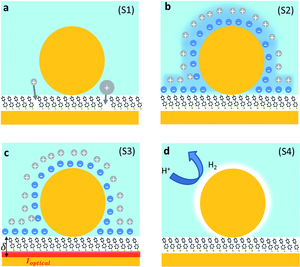 | ||
| Fig. 2 Different scenarios for NPoM reconfiguration with applied potential. (a) Ion penetration into the SAM (S1), (b) potential-driven movement of the double layer changing the local refractive index (S2), (c) individual ionic charges in the solvated double layer just above the Au surface modulating the surface conductivity (S3), and (d) H+ reduction to form H2 gas locally around the NP (S4). | ||
A second scenario (S2) would involve the potential-driven movement of the double layer changing the local refractive index in the vicinity of the gap enough to tune the plasmons (Fig. 2b). As the modulation of the refractive index in bulk salt solutions is expected to be small11 (Δn ≪ 0.1 for 0.5 mM of NaCl) this would be predicted to result in small spectral shifts. Changes in the refractive index in the immediate vicinity of the NP give a linear spectral shift of 45 nm RIU−1 (Fig. 3a).
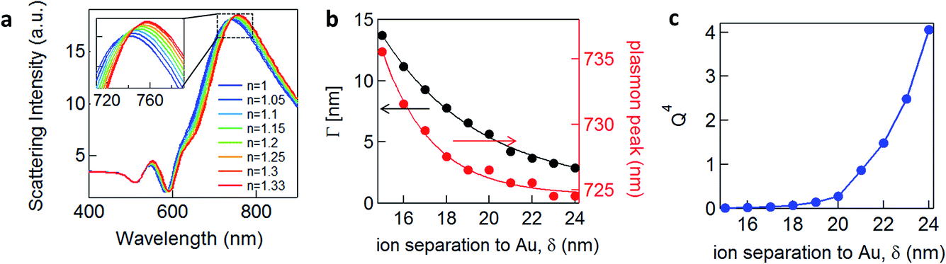 | ||
| Fig. 3 Plasmonic tuning of scattering and SERS by applied potential. (a) Simulated plasmonic response (COMSOL) of 80 nm NPoM with 1.5 nm shell with refractive index from n = 1 (blue) to n = 1.33 (red). Overall shift Δλ ∼ 15 nm. (b) Calculated peak width Γ due to Drude damping (black), and calculated coupled plasmon peak wavelength (red), vs. ion separation to gold. (c) Quality factor of plasmonic resonance, Q4, vs. ion separation to gold. | ||
We now explore a third possibility (S3) where the surface currents which drive the plasmons are modulated by ionic charges in the solvated double layer just above the Au surface (Fig. 2c, red sheet). To build a simple analytical model to track this, we consider surface conduction in a thin sheet, borrowing from the analogous situation of a 2D electron gas within an inorganic semiconductor such as GaAs or Si whose resistivity is modulated by remote charges at a distance δ above the Au surface (here solvated ions of density ni). Electron scattering in the Au surface sheet depends strongly on δ so that only the most tightly-bound ions in the inner Helmholtz layer are considered (Fig. 2c). This model12 yields Au conductivity σ = neμ = 1/ρ, where the electron mobility μ = (8e/πℏni)(kFδ)3 with the Fermi wavevector kF = (3π2n)1/3 set by the Au electron density n. As we will show, using realistic values for these parameters shows that negative voltages which increase the ion separation, δ, lead to blue shifts and line broadening (Fig. 3b), as observed in recent experiments.13–15 Thus modulation of the double layer changes the surface conductivity of gold, thereby modifying the plasmonic coupling.
To quantify the spectral and SERS changes expected from this modulation of the surface conductivity, we employ an analytic circuit model for coupled plasmonic dimers separated by small gaps developed by Benz et al.16 The normalised gap capacitance η is given by η = Cg/Cs = ng2![[thin space (1/6-em)]](https://www.rsc.org/images/entities/char_2009.gif) ln(1 + RΘ2/d), with Cg representing the gap capacitance of the coupled system, Cs the sphere capacitance due to the fringing field, ng the gap refractive index, R the NP radius, d the separation between the nanoparticle and gold film, and Θ ∼ 0.1π is an angle parameterising the laterally localised electric field.
ln(1 + RΘ2/d), with Cg representing the gap capacitance of the coupled system, Cs the sphere capacitance due to the fringing field, ng the gap refractive index, R the NP radius, d the separation between the nanoparticle and gold film, and Θ ∼ 0.1π is an angle parameterising the laterally localised electric field.
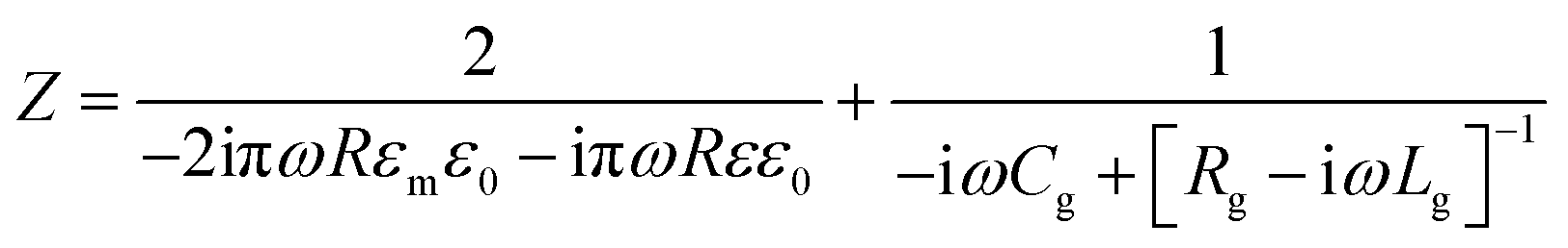
The impedance of the dimer can be written as16
where
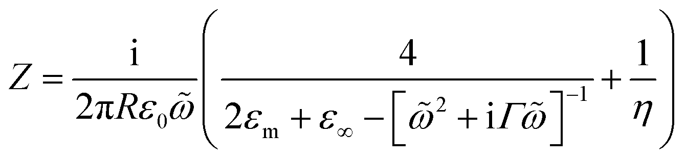
![[small omega, Greek, tilde]](https://www.rsc.org/images/entities/i_char_e10f.gif) = ω/ωp and the damping term is given by Γ = ε0ωpρ(V), with ωp representing the plasma frequency and ρ(V) the potential dependent Au resistivity. From Z we can extract the plasmon resonance peak wavelength and peak width for different ion separations from Au, δ (Fig. 3b).
= ω/ωp and the damping term is given by Γ = ε0ωpρ(V), with ωp representing the plasma frequency and ρ(V) the potential dependent Au resistivity. From Z we can extract the plasmon resonance peak wavelength and peak width for different ion separations from Au, δ (Fig. 3b).
We see that for increasing δ, the peak wavelength blue shifts and gives a sharper plasmonic resonant peak, meaning that this damping contribution is reduced. As we show below, this model fairly reproduces the trends we observe experimentally, as well as those recently obtained on nanoparticles in solution.13 It predicts that the more negatively charged the substrate is, the more blue-shifted and less damped the plasmonic resonance should appear, because the solvated surface ions scatter the electrons accelerated by the light at the Au surface less. The damping term Γ (Fig. 3b) incorporates only the Drude damping contribution and underestimates the overall experimental damping, which broadens the plasmon resonance observed. However, if applying a potential only varies the ion separation and thus the Drude damping, all other contributions to the overall damping should not be modified. Therefore we believe this gives a reasonable estimate of the tuning in peak width, as indeed also observed (see below). We note that this model suggests that in order to observe 10 nm plasmonic shifts from this model, unfeasibly large ion separations from the surface are needed, i.e. >10 nm, while the Debye lengths for the double layer are typically <1 nm.
A corollary of this mechanism, which reduces the Drude damping as the solvated ions retract from the surface, is the increase of the trapped optical field strength, thus also increasing the SERS signal. This SERS strength would scale through a figure of merit proportional to Q4, set by the Q factor of the resonance (Fig. 3c).17,18 An enhancement of the SERS signal should then be observed for negative applied potentials and correspondingly a reduction for positive potentials.3 We note that because we do not include the additional contributions to the damping discussed above, this SERS dependence is overestimated. Our model would also suggest that enhancement of the SERS should be seen for insulating as well as conducting molecules.
Finally, we consider a scenario (S4) exploring the effect of the reversible reduction of H+ in the aqueous solution to form H2 gas which is surface bound around the NP. This can be modelled as a thin shell of gas around the NP with a refractive index n ≃ 1. Using a finite-element calculation, we estimate that this would yield a shift of the coupled plasmonic of ∼15 nm (Fig. 3a) with only minor changes to the SERS intensity.19
To explore these effects experimentally, we exploit the high sensitivity to field-induced changes occurring in the nano-gap to investigate resonant light scattering under a changing electric potential.13 For dark-field spectroscopy, white light irradiates single nanoparticles (average separation of >5 μm) through a high numerical aperture (NA 0.8) 50× objective, with scattered light detected by a fibre-coupled cooled spectrometer. For SERS measurements we selectively illuminate single nanoparticles with a continuous wave (CW) laser at λ = 633 nm (see Methods). When a potential is applied, a transient cathodic current is observed due to the migration of ions in the solution. However, as the ions reach the double-layer equilibrium configuration, the cathodic current reduces (Fig. 4a).
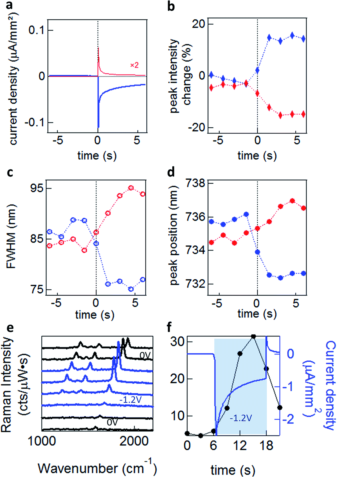 | ||
| Fig. 4 Dynamics under an applied potential. (a) Current density corresponding to applied square wave voltages for 0 V ↔ −1.2 V (blue) and 0 V ↔ +0.3 V (red), measured vs. a Pt pseudo-reference electrode. (b, c and d) Dynamics of dark-field scattering for NPoM with biphenyl-4,4′-dithiol (BPDT) spacer in 0.1 M MgSO4, revealing changes in the (b) peak intensity, (c) resonance full width at half maximum (FWHM), and (d) spectral position of the coupled plasmon mode for the negative (blue) or positive (red) voltages. (e and f) SERS intensity time evolution under an applied voltage of 0 V (black) ↔ −1.2 V (blue), and (f) the corresponding 1578 cm−1 peak intensity enhancement (black) and measured current density (blue). | ||
Significant increases in the coupled peak intensity, together with peak sharpening and spectral blue shifts, are observed when a negative voltage (Au substrate negatively charged) is applied (Fig. 4b–d). The opposite behaviour is observed (decreased amplitude, broadening, and red shifts) for a positive potential. No significant differences are observed between different electrolytes (TBA, MgSO4, NaNO3 and Na2SO4)13 which disproves the ion penetration scenario (S1). Nor are significant differences in plasmon shifts seen between self-assembled monolayers of different conductivity.13 Similar behaviour is seen for many different types of NPoM showing this is a very general behaviour. The dynamics observed for double-layer charging show a sharp initial current spike, saturating after ∼2 s (Fig. 4a). This is in contrast to the scattering spectral changes (Fig. 4b–d) and SERS enhancements (Fig. 4e and f) which give a much slower response with no rapid spike. This suggests that double-layer charging is not directly involved in the modulation of the plasmonic surface (S3). The SERS lines do not shift or disappear, implying that the molecules are not stripped from the Au surface at these potentials, as expected.
We experimentally observe plasmon shifts of the order of 5 to 10 nm, which is not compatible with the modulation of the refractive index in bulk salt solutions (S2), since it would have to change by an unfeasible Δn = 0.1 to explain the spectral shifts observed. This observed shift is however more compatible with the refractive index change induced by a thin layer of H2 gas around the NP (S4). In this scenario however, it is not directly obvious why a 5-fold SERS enhancement is observed (Fig. 4e and f). As we show elsewhere,13 we believe that the previously established idea that the AuNP and the Au surface are at the same potential is in fact incorrect, and field-induced modulation of the molecular SERS is responsible. The spectral shifts on the other hand seem to arise from electrochemical surface reactions in water at the Au NP, which reversibly form and oxidise H2, thus modulating the plasmonic response. Since the SAM layers used are hydrophobic, we do not believe that any such gas evolution can take place in the nanoscale gap, but instead is located on the upper uncoated surfaces of the NP. Because an initial positive voltage already red-shifts the plasmon, this would suggest that already reduced H2 gas is already present as a surface layer. It is however also possible that modulation of the Au conductivity from the local solvated ions (S3) also plays a role.
In conclusion, we study the optical response of Au NPs in a NPoM geometry, separated from bulk Au electrodes by an ultrathin molecular spacer in an electrochemical solution. We study the behaviour of these NPoMs in electrochemical cells considering four different scenarios: ion penetration into the SAM, potential-driven movement of the double layer changing the local refractive index, electronic coulombic scattering from individual ionic charges in the solvated double layer just above the Au surface modulating the plasmonic resonance, and low refractive index H2 gas formation around the NP. We discuss their consequences to the scattering and SERS signatures providing a comparison with experimental data. Currently only the latter two scenarios which have not been previously considered can account for some of the observations, but a unique account of the phenomena is not yet possible. The intriguing phenomena observed here suggest the widespread promise in exploring the electrochemical response of different molecules using SERS, for instance exploring the redox activity of proteins in lipid bilayers combined into this plasmonic geometry.20 Similarly, many surface electrochemical phenomena in inorganic systems are also accessible, such as classic redox phenomena, but observed on the nanoscale. Combining plasmonics with electrochemistry thus opens new dimensions for SERS.21,22
Methods
Electrochemical cell assembly
The Au substrate (working electrode) is sandwiched between an 8–12 Ω indium-tin-oxide (ITO)-coated glass coverslip (counter electrode) and a glass microscope coverslip. The electrochemical cell is assembled so that half of the substrate is immersed in liquid while the other half is dry and electrically contacted with copper tape. A Pt wire (pseudo-reference electrode, 0.5 mm diameter) is inserted into the electrochemical cell and immersed in the aqueous solution. The potentiostat is an Ivium Technologies (CompactStat.h).Dark-field spectroscopy
Optical dark-field images are recorded on a custom Olympus GX51 inverted microscope. Samples are illuminated with a focused white light source (halogen lamp). The scattered light is collected through a 50× dark-field objective (LMPLFLN-BD, NA 0.8) and analysed with a fiber-coupled (50 μm optical fiber) Ocean Optics QE65000 cooled spectrometer. We use a standard diffuser as a reference to normalize white light scattering.SERS analysis
SERS experiments are performed on the same modified Olympus GX51 inverted microscope used for dark-field spectroscopy. A monochromatic 633 nm HeNe laser beam is focused on the sample using a 50× objective (NA 0.8). Raman scattering is collected through the center of the objective and analysed with a Shamrock SR-303i spectrometer (600 l mm−1 650 nm blazed grating) coupled with an EMCCD camera cooled to −85 °C. Rayleigh scattering is filtered out with a long pass 633 nm filter. The system is calibrated using a silicon substrate as a reference. Spectral acquisitions are taken using an integration time of 1 s and the laser power on the sample is 30 μW.Numerical simulation
Finite-element simulations are performed with COMSOL for an 80 nm Au NP, with a 1.5 nm shell with a refractive index from n = 1 to n = 1.33, a spacer with a thickness of 1.8 nm and refractive index n′ = 1.38, and a surrounding medium refractive index n′′ = 1.3.Acknowledgements
We acknowledge financial support from EPSRC grant EP/G060649/1, EP/L027151/1, EP/G037221/1, EPSRC NanoDTC, and ERC grant LINASS 320503. C. T. was supported by funding from the People Programme (Marie Curie Actions) of the European Union’s Seventh Framework Programme (FP7/2007–2013) under REA grant agreement number 609405 (COFUNDPostdocDTU).References
- D. M. Adams, L. Brus, C. E. D. Chidsey, S. Creager, C. Creutz, C. R. Kagan, P. V. Kamat, M. Lieberman, S. Lindsay, R. A. Marcus, R. M. Metzger, M. E. Michel-Beyerle, J. R. Miller, M. D. Newton, D. R. Rolison, O. Sankey, K. S. Schanze, J. Yardley and X. Zhu, J. Phys. Chem. B, 2003, 107(28), 6668–6697 CrossRef CAS.
- C. R. Bradbury, J. Zhao and D. J. Fermín, J. Phys. Chem. C, 2008, 112(27), 10153–10160 CAS.
- J. Zhao, M. Wasem, C. R. Bradbury and D. J. Fermín, J. Phys. Chem. C, 2008, 112(18), 7284–7289 CAS.
- J. Zhao, C. R. Bradbury and D. J. Fermín, J. Phys. Chem. C, 2008, 112(17), 6832–6841 CAS.
- J.-N. Chazalviel and P. Allongue, J. Am. Chem. Soc., 2011, 133(4), 762–764 CrossRef CAS PubMed.
- X. Xiao, F.-R. F. Fan, J. Zhou and A. J. Bard, J. Am. Chem. Soc., 2008, 130(49), 16669–16677 CrossRef CAS PubMed.
- F.-R. F. Fan and A. J. Bard, Science, 1997, 277(5333), 1791–1793 CrossRef CAS.
- J. Meier, J. Schiøtz, P. Liu, J. K. Nørskov and U. Stimming, Chem. Phys. Lett., 2004, 390(4–6), 440–444 CrossRef CAS.
- C. P. Byers, B. S. Hoener, W.-S. Chang, M. Yorulmaz, S. Link and C. F. Landes, J. Phys. Chem. B, 2014, 118(49), 14047–14055 CrossRef CAS PubMed.
- N. Yamamoto, S. Ohtani and F. J. García de Abajo, Nano Lett., 2011, 11(1), 91–95 CrossRef CAS PubMed.
- V. Lioubimov, A. Kolomenskii, A. Mershin, D. V. Nanopoulos and H. A. Schuessler, Appl. Opt., 2004, 43(17), 3426–3432 CrossRef CAS PubMed.
- S. Das Sarma, E. H. Hwang, S. Kodiyalam, L. N. Pfeiffer and K. W. West, Phys. Rev. B: Condens. Matter Mater. Phys., 2015, 91(20), 205304 CrossRef.
- G. Di Martino, et al. , Nano Lett., 2017, 17, 4840 CrossRef CAS PubMed.
- S. S. E. Collins, X. Wei, T. G. McKenzie, A. M. Funston and P. Mulvaney, Nano Lett., 2016, 16(11), 6863–6869 CrossRef CAS PubMed.
- A. M. Brown, M. T. Sheldon and H. A. Atwater, ACS Photonics, 2015, 2(4), 459–464 CrossRef CAS.
- F. Benz, B. de Nijs, C. Tserkezis, R. Chikkaraddy, D. O. Sigle, L. Pukenas, S. D. Evans, J. Aizpurua and J. J. Baumberg, Opt. Express, 2015, 23(26), 33255–33269 CrossRef CAS PubMed.
- K. Kneipp, Y. Wang, H. Kneipp, L. T. Perelman, I. Itzkan, R. R. Dasari and M. S. Feld, Phys. Rev. Lett., 1997, 78(9), 1667–1670 CrossRef CAS.
- V. M. Shalaev, E. Y. Poliakov and V. A. Markel, Phys. Rev. B: Condens. Matter Mater. Phys., 1996, 53(5), 2437–2449 CrossRef CAS.
- A. Lombardi, A. Demetriadou, L. Weller, P. Andrae, F. Benz, R. Chikkaraddy, J. Aizpurua and J. J. Baumberg, ACS Photonics, 2016, 3(3), 471–477 CrossRef CAS PubMed.
- R. W. Taylor, F. Benz, D. O. Sigle, R. W. Bowman, P. Bao, J. S. Roth, G. R. Heath, S. D. Evans and J. J. Baumberg, Sci. Rep., 2014, 4, 5940 CrossRef CAS PubMed.
- J.-H. Zhong, X. Jin, L. Meng, X. Wang, H.-S. Su, Z.-L. Yang, C. T. Williams and B. Ren, Nat. Nanotechnol., 2017, 12(2), 132–136 CrossRef CAS PubMed.
- Z.-C. Zeng, S.-C. Huang, D.-Y. Wu, L.-Y. Meng, M.-H. Li, T.-X. Huang, J.-H. Zhong, X. Wang, Z.-L. Yang and B. Ren, J. Am. Chem. Soc., 2015, 137(37), 11928–11931 CrossRef CAS PubMed.
| This journal is © The Royal Society of Chemistry 2017 |