 Open Access Article
 This Open Access Article is licensed under a
 Creative Commons Attribution 3.0 Unported Licence
Designing porous electronic thin-film devices: band offsets and heteroepitaxy
Keith T.
Butler
 *a,
Christopher H.
Hendon
b and
Aron
Walsh
cd
*a,
Christopher H.
Hendon
b and
Aron
Walsh
cd
aDepartment of Chemistry, University of Bath, BA2 7AY, UK. E-mail: k.t.butler@bath.ac.uk
bDepartment of Chemistry, Massachusetts Institute of Technology, Cambridge, Massachusetts 02139, USA
cDepartment of Materials, Imperial College London, Exhibition Road, London, SW7 2AZ, UK
dDepartment of Materials Science and Engineering, Yonsei University, Seoul, South Korea
First published on 16th June 2017
Abstract
Increasing numbers of electrically active porous framework materials are being reported, with conductivities that make them attractive for technological applications. As design strategies for efficient carrier transport emerge, the next challenge is to incorporate the materials into a functioning device. In thin-film devices interface effects are of critical importance to overall function. In this article we present a method to identify compatible materials combinations to achieve mechanically robust, electronically optimal pairings. The computational screening is based on a two-step procedure: (i) matching of lattice constants to ensure interfaces with minimal epitaxial strain and therefore maximal mechanical and chemical stability; (ii) matching of absolute electron energies to construct energy-band-alignment diagrams, which can be used to screen for particular electronic applications. We apply the methodology to search for zeolitic imidazolate framework (ZIF) type materials that are compatible with native metal electrodes. The procedure allows us to predict simple routes for electrochemical deposition of ZIFs for application as conductive porous electrodes.
1 Introduction
The field of metal organic frameworks (MOFs) has witnessed a spectacular proliferation of research since their first discovery some 30 years ago.1 Initially, interest in these materials was focussed on a drive towards exploiting the porous geometry and tuneable chemistry of MOFs for applications such as gas storage, gas separation and heterogeneous catalysis.2–7 The past decade has seen a steady rise in the number of studies reporting the synthesis and characterisation of electrically conductive MOFs.8–10 This development has lead to much excitement and speculation about possible disruptive technological advances, enabled by coupling the porosity and geometrical tuneability of MOFs with electrical conductivity. For example, researchers have reported supercapacitors with large capacity and turnover rates based on porous MOFs;11,12 moreover, concepts such as electrically driven catalytic sites and porous field effect transistors have continued to fire the imagination and fuel research in this field.13,14 Despite the large strides in recent years, the realisation of truly functional MOF semiconductor devices faces several key challenges in order to displace existing materials.In order to realise MOF semiconductor devices, not only conductive MOFs, but also effective interfaces with other components must be realised. As Herbert Kromer noted, when discussing modern microelectronics, “the interface is the device”. In particular interfaces should be well matched both structurally and electronically. The former requires two materials with compatible crystal lattices to ensure defect-free growth; the latter requires frontier electron energy levels (ionisation potentials and electron affinities) commensurate with the required application. The chemical diversity and tuneability of MOFs means that engineering both geometric and electronic structure to grow desired device configurations is possible. Reticular synthesis has elegantly and consistently demonstrated the ability to control geometry.15,16 Substitution and manipulation of both ligand and linker groups also allows for the fine-tuning of electronic and optical properties.14 Nevertheless, the realisation of MOF electronics remains in its infancy.
Of the recent advances in MOF technology which make MOF semiconductor applications closer to a reality, the ability to grow thin films of materials in device architectures is one of the key developments. Several routes exist for the deposition of MOF thin films, including solvo-thermal routes such as liquid phase epitaxy (LPE), layer-by-layer addition and suspension array techniques;17–20 however, such routes are often difficult to achieve and can result in poor quality film growth. Such problems are not so serious depending on the intended application of the film, but for electronics applications the growth of high-quality uniform films is critical. One successful route for achieving the growth of MOF films from the liquid phase makes use of a self-assembled monolayer (SAM) to direct the growth of the MOF on the substrate. This approach, first demonstrated by Scholl and Fischer,19 has the virtue of mediating strain, resulting from lattice mismatch between the MOF and substrate. But in an electronic device context the presence of such a SAM could lead to formation of an unwanted electrostatic potential barrier to charge transport between the MOF and substrate.
The work of Ameloot and co-workers powerfully demonstrates how fabrication techniques developed in the microelectronics industry, namely chemical vapour deposition (CVD) and atomic layer deposition (ALD) can be applied to the growth of high-quality thin films of MOFs for electronics applications.21 In this approach a metal oxide is first deposited on the substrate by ALD. The metal oxide is then converted to the MOF – in the published example ZIF-8 was used – which is then transformed to a framework by CVD. This allows for the formation of a uniform crystalline interface consisting of a MOF and substrate in direct contact.
In the context of porous frameworks with modular components and the myriad desired device architectures, computational modelling and screening can offer guidance in the choice of substrate and framework. In this contribution we demonstrate a practical and general screening procedure for optimal interfaces that draws from methods recently developed by us for semiconductor junction design22 and the frontier electron energy evaluation of porous solids.23,24 All codes used and developed in this work are freely available, with worked examples as part of the SMACT package for semiconductor design.25 The synthesis and design of hybrid frameworks is a complex process, dependent on many factors;26,27 however, the tools proposed in this study can help to navigate the complex space of possible substrate/framework combinations for thin film growth.
We first outline the chemical principles and present the methods developed for interface matching and electron energy evaluation. We then show how these procedures can be combined for high-throughput screening. We use the procedure to evaluate the growth of a series of zeolitic imidazolate frameworks (ZIFs) on metal substrates, comparing them to recent experimental results to highlight the utility of the procedure, predicting optimal substrate/framework combinations.
2 Methods and screening procedure
2.1 Identification of framework growth planes
Before matching the lattice parameters of the materials that form a heterojunction, it is desirable to have an idea of the potential planes along which the material can be expected to grow. For traditional solid-state compounds, it is common to calculate the surface energies of the crystal, which is the energy required to cleave a surface in a given orientation. This has been done for a wide range of simple metals and compound semiconductors.29–32 By applying the Gibbs–Wulff theorem one can also construct representative morphologies of the crystal with the shape determined by the ratio of the energies of the various crystal cleaves. In a MOF the same procedure is, in principle, possible; however, the sheer size of the calculations required to calculate the surface structures of MOFs makes this intractable to all but the most approximate total energy calculation approaches. In addition, while thermodynamically-controlled morphology can be expected for high temperature synthesis, for solution based growth the crystal growth is likely to be directed by chemical kinetics.To allow for a high-throughput approach to enumerating potential growth directions we consider simple geometric models of the materials. In this case we consider that a growth direction is allowed if, and only if, a plane in that direction can be drawn such that it does not intersect any of the linker polyhedra that form the structure. An example of an allowed and forbidden plane is shown in Fig. 1. By casting the structure as a simplified collection of linker polyhedra we use the METADISE code33 to systematically sort between allowed and forbidden growth directions.
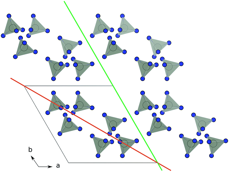 | ||
| Fig. 1 Schematic of identifying growth planes in ZIF-8. The organic linkers are suppressed and lighting is turned out in VESTA28 for clarity. Orange: the (110) plane is not allowed, as it cannot be drawn without dissecting linker units. Green: the (100) plane is allowed as it can be drawn without dissecting linker unit. | ||
2.2 Epitaxial matching of framework and substrate
An epitaxial matching procedure can be applied to search through the allowed planes of the substrate and MOF to identify lattice parameter matching. Highly mismatched lattices result in significant strain at the interface; this is detrimental for a number of reasons. In certain cases the strain will alleviate itself by the formation of dislocations at the interface, whereby a half-plane of one of the materials is missing, and this is described as a semi-coherent interface. Electronically, these misfit dislocations can result in electron–hole recombination centres, which are detrimental to performance. Mechanically, the dislocations act as centres for junction degradation. If the lattice mismatch is greater still the interface is typically described as incoherent. Incoherent interfaces are associated with high formation energies and poor mechanical and electronic properties.In cases where the crystal structure of the two materials forming the interface are the same, the lattice mismatch can simply be calculated by comparing the lattice parameters of the two materials. However, when the junction is between materials with different structure – as in the case of MOF thin films – the situation is more complex. Zur and McGill proposed a scheme34 whereby two lattices are said to match if the interface translational symmetry could be compatible with the symmetry on both sides of the interface. The lattice matching at the interface is characterised by the match between the lattice parameters and the number of unit cells required to achieve the lowest mismatch in lattice constants.
For example, consider an interface AB, if material A has a lattice constant of 4 and material B has a lattice constant of 3, then there is a 25% mismatch between the 1![[thin space (1/6-em)]](https://www.rsc.org/images/entities/char_2009.gif) :1 interface; however, if we consider a 3× expansion of A and a 4× expansion of B the lattice mismatch is now 0%. Allowing sufficient expansions of either material will result in perfect matching for any pair of materials with commensurate symmetry. However, as the number of expansions increases, there is an associated increased chemical bonding mismatch between the layers.22,34 Larger expansions also necessitate the existence of substrates with large pristine surface areas for growth, and therefore the number of expansions should be limited. In this work we consider expansions of up to 20 times the unit cell of either material. This number is greater than we have previously applied for matching semiconductor junctions22,35 and reflects the typically large unit cells found in hybrid frameworks, which necessitate expansions of the substrate to accommodate even one expansion of the MOF.
:1 interface; however, if we consider a 3× expansion of A and a 4× expansion of B the lattice mismatch is now 0%. Allowing sufficient expansions of either material will result in perfect matching for any pair of materials with commensurate symmetry. However, as the number of expansions increases, there is an associated increased chemical bonding mismatch between the layers.22,34 Larger expansions also necessitate the existence of substrates with large pristine surface areas for growth, and therefore the number of expansions should be limited. In this work we consider expansions of up to 20 times the unit cell of either material. This number is greater than we have previously applied for matching semiconductor junctions22,35 and reflects the typically large unit cells found in hybrid frameworks, which necessitate expansions of the substrate to accommodate even one expansion of the MOF.
2.3 Chemical similarity of framework and substrate
In previous work considering semiconductor heterojunctions we characterised the goodness of fit of two materials, including an atomic site overlap (ASO) parameter.22 The ASO accounts for the difference in coordination number between the interface and the pristine bulk materials by considering rigid translations of the occupied sites of the interface layers of the two materials. For framework materials on a dense substrate the ASO is not appropriate for a number of reasons. First, the porous nature of the framework means that there will be significantly more under-coordinated sites on the substrate. Often these under-coordinated sites will be compensated by protons or hydroxyls depending on the pH of the system, which cannot be accounted for by the ASO. Second, the framework flexibility means that the lattice sites are more pliable than those in a traditional solid-state lattice; therefore, the rigid translation of lattice sites is a less valid approximation.Here, we instead consider the chemical similarity of the substrate and the linker metal (cations) as a metric for assessing the suitability of a given framework/solid pairing. The similarity is described as the difference in Pearson hardness between the metals in the two environments.36,37 The Pearson hardness
 | (1) |
For example, consider a Cu(II) based MOF (such as HKUST-1) growing on substrates of Al2O3, ZnO and CuO. From a chemical perspective, CuO would be expected to provide the best substrate as the difference between the metals is zero, ZnO would be next most favourable as the Zn(II) cation has a Pearson hardness of 10.88, closer to that of Cu(II) (8.27) than that of Al(III) (45.77). By including the chemical similarity as well as lattice matching we can take account of some of the complex chemistry as well as the purely mechanical aspects of interface matching. Additional factors such as wettability, surface roughness and acidity/basicity of the surface are also known to be important in determining the chemistry and growth of thin films on MOF surfaces and could be included in any further screening studies.38
2.4 Band alignment
To assess electronic matching requires the most computationally intensive part of the screening procedure: first-principles quantum mechanical calculations. All procedures performed here are available as automated and editable Python scripts, developed using the Atomistic Simulation Environment (ASE). Crystal structures were optimised using total energy and forces calculated from Kohn–Sham density functional theory as implemented in VASP39 within the projector augmented wave (PAW) formalism.40 The PBEsol functional41 was used for structural optimisation, with a plane-wave cutoff energy of 500 eV to define the basis set and Gamma point sampling of the Brillouin zone. The structures were relaxed (volume and ionic positions) until forces on all atoms were reduced to below 10−2 eV A−1.To calculate accurate electron energies we then applied a hybrid exchange-correlation functional (HSE06),42 which corrects for spurious electron self-interaction by including a fraction of screened Hartree–Fock exact exchange. From these calculations we also obtained the electrostatic potential of the crystal, which is used to place the electron energies on an exact scale as outlined below, using the MacroDensity package.
The electron energies obtained from periodic electronic structure calculations contain an arbitrary offset in the average electrostatic potential, due to the boundary conditions applied in the Ewald summation. This offset does not affect the total energy of the system, but means that frontier electron energies obtained for different materials cannot be compared directly. In order to circumvent this limitation, a well-defined reference potential is required. We have shown previously that the electrostatic potential at the centre of a MOF pore provides a vacuum level potential, which should be equivalent for all systems.23 By referencing the eigenvalues obtained from the electronic structure calculation to this vacuum level, we can then compare the valence and conduction band energies between systems. The workfunctions of the metals were taken from literature.43
When the absolute band energies have been calculated they can be used as a criterion for screening for suitable combinations of materials. The desired matching of energy levels will depend on the application in question. For example, if the framework is to be applied as a low κ barrier in microelectronics, then a large offset between the valence and conduction band of the MOF and those of the semiconductor component would be required. On the other hand, if the MOF is to act as an active layer in a device such as a transistor, photovoltaic or capacitor then as small as possible a barrier is desired at the junction. Indeed, semiconductor physics provides a figure of merit for contacts between active layers in a device, the contact resistance:
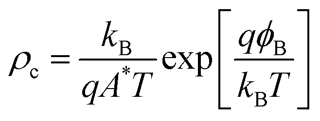 | (2) |
The value depends exponentially on the electrical barrier at the junction (ϕB), as well as the Boltzmann constant (kB), carrier charge (q), Richardson constant (A*), and the temperature (T). As demonstrated by Anderson,44ϕB can be estimated to a first approximation as the difference between the band energies in each material. For electron transport it is the difference in electron affinities (EAs), for hole transport it is the difference between the ionisation potentials (IPs). It has been shown that the exact value of this barrier can be sensitive to the details of the interfaces,45,46 as well as the electron energies of the constituent materials; however, for the purpose of a first screening, the application of Anderson’s rule represents an acceptable trade-off between accuracy and cost of computation.
3 Results
We now apply the above procedure outlined above to investigate the heterojunction formed between a series of ZIF materials and metal electrodes. This example is of technological relevance as ZIFs deposited on metal electrodes have been demonstrated to have potential application as supercapacitors and can be deposited via the anodic dissolution method, allowing direct growth of the framework on a solid substrate. We consider 3 Zn(II) based(ZIF-7, ZIF-8, ZIF14) and 2 Co(II) based (ZIF-9, ZIF-67) ZIFs, each deposited on an electrode of the same metal as present in the framework.3.1 Identification of growth planes
We start from a set of all low index planes of the materials| (i, j, k); ∀ − 1 ≤ i, j, k ≤ 1, | (3) |
| Material | Surface | u/Å | v/Å | θ/° |
|---|---|---|---|---|
| ZIF-7 | (0001) | 14.27 | 14.27 | 72.27 |
(11![[2 with combining macron]](https://www.rsc.org/images/entities/char_0032_0304.gif) 1) 1) |
22.99 | 22.99 | 60.00 | |
| ZIF-8 | (0001) | 14.71 | 14.71 | 70.47 |
| (111) |
24.03 | 24.03 | 60.00 | |
| ZIF-9 | (0001) | 14.25 | 14.25 | 72.77 |
| (111) |
22.94 | 22.94 | 60.00 | |
| ZIF-14 | (112![[1 with combining macron]](https://www.rsc.org/images/entities/char_0031_0304.gif) ) ) |
37.52 | 37.52 | 60.00 |
| (10) |
26.53 | 26.53 | 90.00 | |
| ZIF-67 | (0001) | 14.67 | 14.67 | 70.47 |
| (111) |
23.98 | 23.98 | 60.00 |
3.2 Epitaxial matching
Following a scenario of anodic dissolution growth, we only consider ZIFs growing on the same metal that is present in the framework linkers. In this case both metals form hexagonal packed lattices. The dominant surface for both metals is (0001), therefore we use our matching procedure to search for epitaxial relations between the (0001) surface of the metals and the identified growth planes from the previous step. As stated previously, it is necessary to consider larger surface areas for growth of framework materials than for traditional epitaxial matching between semiconductors and the maximum number of surface cell expansions for the materials is set to 20 here. In all cases we have used experimentally determined lattice parameters for the matching, in order to be consistent with growth conditions. We first consider the growth of the ZIFs on their corresponding parent metal; although the metals generally have a surface layer of oxide in air, under the conditions of electro-deposition in solution the oxide should be largely removed leaving the bare metal, Table 2.| ZIF | Surface | Substrate | Surface | Strain |
|---|---|---|---|---|
| ZIF-7 | (111)2 × 2 |
Zn | (0001)17 × 19 | 1.5% |
| ZIF-7 | (111)2 × 6 |
ZnO | (0001)7 × 20 | 1.1% |
| ZIF-8 | (111)1 × 2 |
Zn | (0001)9 × 19 | 0.2% |
| ZIF-8 | (111)2 × 6 |
ZnO | (0001)15 × 20 | 1.4% |
| ZIF-9 | (111)1 × 2 |
Co | (0001)9 × 20 | 1.6% |
| ZIF-9 | (111)5 × 12 |
CoO | (111)19 × 20 | 0.1% |
| ZIF-67 | (111)2 × 2 |
Co | (0001)19 × 20 | 0.5% |
| ZIF-67 | (111)2 × 2 |
CoO | (111)20 × 20 | 0.5% |
Considering the Co based ZIFs (ZIF-9, and ZIF-67) we find that both frameworks have allowed growth planes that show lattice matching with the substrate with strain below 5% (typically considered a boundary between semi-coherent and incoherent surfaces). A 1 × 2 expansion of the (111) surface of ZIF-9 matches to a 9 × 20 expansion of the Zn (0001) surface with an epitaxial strain of 1.6%. Although this is a relatively high strain, we note that the flexibility of framework materials means that they are likely to accommodate more strain than regular solid-state materials with less defect formation. A 2 × 2 expansion of the ZIF-67 (111) surface matches to a 19 × 20 expansion of the (0001) surface of Zn with considerably better epitaxy (strain = 0.5%). This is an excellent match and, given the chemical compatibility of substrate and framework, is consistent with the observed growth of high-quality films of ZIF-67 on Co anodes via solution deposition.11 Indeed, in another study we recently achieved growth of both ZIF-9 and ZIF-67 films on Co, but the ZIF-9 films were of much lower crystalline quality, consistent with the greater lattice mismatch.
Considering the Zn based ZIFs (ZIF-7 and ZIF-8), again both frameworks have allowed growth planes that show lattice matching to the metal substrate. A 2 × 2 expansion of the ZIF-7 (111) surface matches to a 17 × 19 expansion of the Zn (0001) surface with a mismatch of 1.5%. As with the ZIF-9/Co interface this is a relatively high mismatch. A 1 × 2 expansion of the ZIF-8 (111) surface matches with a 9 × 19 expansion of the Zn (0001) surface with a strain of 0.2%. As with the ZIF-67/Co interface this is a very good lattice match and is close to perfect epitaxy. The results for these Zn based ZIFs are also in agreement with our recent experimental findings, where we observe that ZIF-7 and ZIF-8 both form thin films on Zn via anodic deposition, but that the ZIF-8 crystals are of far greater quality, consistent with better lattice matching.47
Finally, ZIF-14, based on the ethyl imidazolate ligands also has an epitaxially matched growth direction on the (0001) surface of Zn. In this case a 1 × 1 expansion of the (2) surface of ZIF-14 matches to a 14 × 15 expansion of Zn (0001), with a strain of 0.5%, once again commensurate with growth of high-quality films. We now turn our attention to the band alignment between the ZIFs and substrates.
A route to achieving better matching could be the growth of a thin film of metal oxide at the electrode surface. If suitably mild solution conditions were used such an oxide could persist under deposition conditions. We consider this by matching the ZIFs to parent metal-oxides in Table 2. In the case of ZIF-9, it is demonstrated that the matching of framework to substrate can be substantially improved by allowing a thin layer of oxide to form. It is interesting to note that this approach of application of ultra-thin oxide films can also be used to tune electronic alignment, by altering interface dipoles,46 raising the possibility of tailored multilayer MOF/metal-oxide/metal structures.
3.3 Electronic matching
The valence and conduction band offsets are presented in Fig. 2 along with the workfunctions of the metal electrodes. This diagram shows that a combination of the linker and the ligand play a role in determining the band edge positions. ZIF-14, the only framework based on the ethyl imidazolate ligand, has the deepest ionisation potential. Of the two Co(II) based frameworks, the methyl imidazolate based ZIF-7 has a deeper IP than the benzyl imidazolate based ZIF-9. Similarly the methyl imidazolate based Zn(II) ZIF-8 has a deeper IP than the benzyl imidazolate based ZIF-67. The presence of unpaired d-electrons in Co, which are less tightly bound, also has an effect of reducing the IPs. Hence, ZIF-7 has a lower IP than ZIF-8 and ZIF-9 has a lower IP than ZIF-67. The electron affinity values are more closely related to the ligand species, both methyl imidazolate ZIFs (7 and 8) have by far the shallowest EAs. The metal species does affect the EA though, with the Co based ZIFs (7 and 9) having deeper EAs than their Zn based counterparts (8 and 67, respectively). This contribution can be related to the presence of empty d-states for hybridising with the unoccupied ligand orbitals.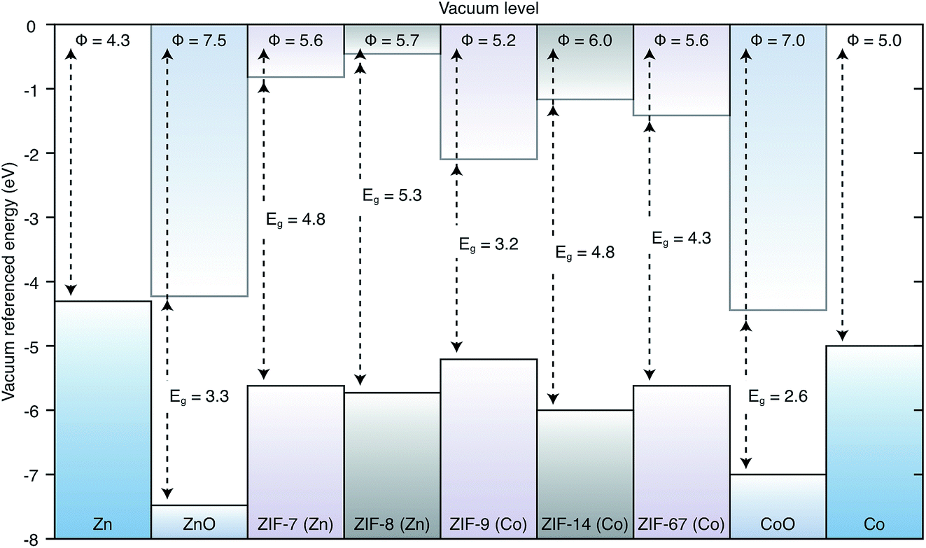 | ||
| Fig. 2 Band alignment of ZIFs. IPs (ϕ) and band gaps (Eg) are given for each framework and for the metal oxides in units of eV. The workfunctions of the contact metals are given at either end. The label of each framework indicates the metal linker node upon which it is based. | ||
In all cases these materials present significant barriers to electron injection from the metal to the framework. The lowest barrier to injection of electrons from metal to framework, based on Anderson’s rule, is 2.93 eV from Co to ZIF-9, the highest is from Co to ZIF-7 at 4.22 eV. The Zn to ZIF barriers are 3.63 eV, 3.84 eV and 3.88 eV for ZIF-67, -8 and -14 respectively. All of these barriers are high in the context of a functioning device where efficient charge flow is desired. Losses at an electrical junction depend exponentially on this barrier. Equally if one were considering the extraction of electrons from the conduction band of the framework to the metals, these offsets mean that there would be an energy loss at the interface.48,49
From the materials considered, some junctions do have reasonable barriers for injection of holes from the metal to the framework, notably the Co(II) frameworks have barriers of 0.61 eV and 0.24 eV for the Co/ZIF-7 and Co/ZIF-9 junctions respectively. The Zn(II) frameworks have barriers of 1.44 eV, 1.32 eV and 1.65 eV for the Zn/ZIF-8, Zn/ZIF-67 and Zn/ZIF-14 junctions, respectively. Based on the results of these alignments, in the absence of any other information about lattice and chemical compatibility presented earlier we are able to suggest that for application in a device where the ZIF would be an electrically active layer, the Co(II) based frameworks are best suited and a device architecture where holes flow from the metal to the framework would be the most efficient setup.
4 Discussion
For the growth of ZIF thin-films by anodic deposition, our screening procedure shows that all of the frameworks considered in this study are compatible with their respective parent metal electrodes. Chemically the frameworks and substrates are well suited, which may be expected as the metal in the framework is derived from the substrate. The ZIFs based on benzyl imidazolate and methyl imidazolate were found to have the same allowed growth directions, whilst ZIF-14, based on the ethyl imidazolate ligand, has a different topology, resulting in different allowed growth directions. All of the frameworks have allowed growth directions that are compatible with the dominant metal surface. However, some of the frameworks have significantly better lattice matching than others, notably ZIF-8 is better than ZIF-7 for Zn growth and ZIF-67 is better than ZIF-9 for Co growth. These results correlate well with the observed crystalline quality of thin films of these materials prepared by anodic deposition experimentally.For electronic applications we found that the conduction band alignment suggests that electron injection from the metal to the framework in many cases presents a large barrier, precluding any application where efficient current flow in that direction is required. However, the barriers to hole injection from metal to framework are significantly lower and in many cases within acceptable limits for device applications. In particular the Co based frameworks align well with the workfunction of Co metal, with barriers of 0.24 eV and 0.62 eV for ZIF-9 and ZIF-67 respectively. In choosing between ZIF-9 and ZIF-67 for a potential device application, the relative importance of interfacial charge barriers and film quality should be taken into consideration. Whilst ZIF-9 has a smaller barrier, it also has a larger lattice mismatch and hence poorer quality films. In general, once the barrier heights are within a reasonable range, the quality of the film will be more important, as it determines the stability of the architecture and the charge carrier transport qualities of the film. Therefore, ZIF-67 is a better choice of framework for Co than ZIF-9.
5 Conclusions
We have presented a practical computational procedure for predicting optimal pairings of MOF and substrate for thin-film growth. The procedure relies on matching the geometry, chemistry and electronic structure of the framework/substrate pair, in a systematic manner. We have applied our procedure to a set of zeolitic imidazolate frameworks, which can be grown by anodic deposition, obtaining a good agreement between the predicted and observed quality of the film growths. By aligning the electron energies of the materials we are able to show how electron injection from metal to ZIF is difficult, whilst hole injection has a considerably lower barrier.The procedure that we have outlined here is completely general and can be automated in a systematic manner, facilitating high-throughput computational screening for optimal MOF/substrate pairings. With the recent reports of thin-film depositions of MOFs, the development of electroactive hybrid organic–inorganic compounds, and the continuing proliferation of calculated and measured materials properties data, we hope that our method will provide a bridge between these exciting and expanding fields.
Acknowledgements
We acknowledge membership of the U. K.’s HPC Materials Chemistry Consortium (EPSRC EP/L000202) and access to computational resources through PRACE. K. T. B. is funded by the EPSRC (EP/M009580/1 and EP/J017361/1). A. W. acknowledges support from the Royal Society for a University Research Fellowship. C. H. H. made use of the Extreme Science and Engineering Discovery Environment (XSEDE), which is supported by the National Science Foundation (grant number ACI-1053575).References
- O. M. Yaghi, H. Li, M. Eddaoudi and M. O’Keeffe, Nature, 1999, 402, 276–279 CrossRef.
- R. Morris and P. Wheatley, Angew. Chem., Int. Ed., 2008, 47, 4966–4981 CrossRef CAS PubMed.
- S. Ma and H.-C. Zhou, Chem. Commun., 2010, 46, 44–53 RSC.
- J. Duan, W. Jin and S. Kitagawa, Coord. Chem. Rev., 2017, 332, 48–74 CrossRef CAS.
- T.-H. Bae, J. S. Lee, W. Qiu, W. J. Koros, C. W. Jones and S. Nair, Angew. Chem., Int. Ed., 2010, 49, 9863–9866 CrossRef CAS PubMed.
- M. Zhao, S. Ou and C.-D. Wu, Acc. Chem. Res., 2014, 47, 1199–1207 CrossRef CAS PubMed.
- H.-C. Zhou and S. Kitagawa, Chem. Soc. Rev., 2014, 43, 5415–5418 RSC.
- A. A. Talin, A. Centrone, A. C. Ford, M. E. Foster, V. Stavila, P. Haney, R. A. Kinney, V. Szalai, F. El Gabaly, H. P. Yoon, F. Léonard and M. D. Allendorf, Science, 2014, 343, 66–69 CrossRef CAS PubMed.
- L. Sun, C. H. Hendon, M. a. Minier, A. Walsh and M. Dincă, J. Am. Chem. Soc., 2015, 137, 6164–6167 CrossRef CAS PubMed.
- T. C. Narayan, T. Miyakai, S. Seki and M. Dincă, J. Am. Chem. Soc., 2012, 134, 12932–12935 CrossRef CAS PubMed.
- S. D. Worrall, H. Mann, A. Rogers, M. A. Bissett, M. P. Attfield and R. A. Dryfe, Electrochim. Acta, 2016, 197, 228–240 CrossRef CAS.
- D. Sheberla, J. C. Bachman, J. S. Elias, C.-J. Sun, Y. Shao-Horn and M. Dincă, Nat. Mater., 2017, 16, 220–224 CrossRef CAS PubMed.
- G. Wu, J. Huang, Y. Zang, J. He and G. Xu, J. Am. Chem. Soc., 2017, 139, 1360–1363 CrossRef CAS PubMed.
- A. Walsh, K. T. Butler and C. H. Hendon, MRS Bull., 2016, 41, 870–876 CrossRef.
- N. W. Ockwig, O. Delgado-Friedrichs, M. O’Keeffe and O. M. Yaghi, Acc. Chem. Res., 2005, 176–182 CrossRef CAS PubMed.
- O. M. Yaghi, M. O’Keeffe, N. W. Ockwig, H. K. Chae, M. Eddaoudi and J. Kim, Nature, 2003, 423, 705–714 CrossRef CAS PubMed.
- O. Shekhah, J. Liu, R. A. Fischer and C. Wöll, Chem. Soc. Rev., 2011, 40, 1081 RSC.
- H. K. Arslan, O. Shekhah, J. Wohlgemuth, M. Franzreb, R. A. Fischer and C. Wöll, Adv. Funct. Mater., 2011, 21, 4228–4231 CrossRef CAS.
- O. Shekhah, H. Wang, S. Kowarik, F. Schreiber, M. Paulus, M. Tolan, C. Sternemann, F. Evers, D. Zacher, R. A. Fischer and C. Wöll, J. Am. Chem. Soc., 2007, 15118–15119 CrossRef CAS PubMed.
- E. López-Maya, C. Montoro, L. M. Rodríguez-Albelo, S. D. Aznar-Cervantes, A. A. Lozano-Pérez, J. L. Cenís, E. Barea and J. A. R. Navarro, Angew. Chem., 2015, 127, 6894–6898 CrossRef.
- I. Stassen, M. Styles, G. Grenci, H. Gorp, W. Vanderlinden, S. Feyter, P. Falcaro, D. D. Vos, P. Vereecken and R. Ameloot, Nat. Mater., 2015, 15, 304–310 CrossRef PubMed.
- K. T. Butler, Y. Kumagai, F. Oba and A. Walsh, J. Mater. Chem. C, 2016, 4, 1149–1158 RSC.
- K. T. Butler, C. H. Hendon and A. Walsh, J. Am. Chem. Soc., 2014, 136, 2703–2706 CrossRef CAS PubMed.
- K. T. Butler, C. H. Hendon and A. Walsh, ACS Appl. Mater. Interfaces, 2014, 6, 22044–22050 CAS.
- D. Davies, K. Butler, A. Jackson, A. Morris, J. Frost, J. Skelton and A. Walsh, Chem, 2016, 1, 617–627 CAS.
- K. T. Butler, K. Svane, G. Kieslich, A. K. Cheetham and A. Walsh, Phys. Rev. B, 2016, 94, 180103 CrossRef.
- K. T. Butler, A. Walsh, A. K. Cheetham and G. Kieslich, Chem. Sci., 2016, 7, 6316–6324 RSC.
- K. Momma and F. Izumi, J. Appl. Crystallogr., 2011, 44, 1272–1276 CrossRef CAS.
- A. Marmier and S. C. Parker, Phys. Rev. B: Condens. Matter Mater. Phys., 2004, 69, 115409 CrossRef.
- A. Walsh and C. R. A. Catlow, J. Mater. Chem., 2010, 20, 10438 RSC.
- J. H. Harding, D. M. Duffy, M. L. Sushko, P. M. Rodger, D. Quigley and J. A. Elliott, Chem. Rev., 2008, 108, 4823–4854 CrossRef CAS PubMed.
- L. Wang, F. Zhou, Y. S. Meng and G. Ceder, Phys. Rev. B: Condens. Matter Mater. Phys., 2007, 76, 165435 CrossRef.
- G. W. Watson, E. T. Kelsey, N. H. de Leeuw, D. J. Harris and S. C. Parker, J. Chem. Soc., Faraday Trans., 1996, 92, 433 RSC.
- A. Zur and T. C. McGill, J. Appl. Phys., 1984, 55, 378 CrossRef CAS.
- C. H. Hendon, S. T. Hunt, M. Milina, K. T. Butler, A. Walsh and Y. Román-Leshkov, J. Phys. Chem. Lett., 2016, 7, 4475–4482 CrossRef CAS PubMed.
- R. G. Pearson, Inorg. Chem., 1988, 27, 734–740 CrossRef CAS.
- R. G. Pearson, J. Am. Chem. Soc., 1963, 85, 3533–3539 CrossRef CAS.
- P. C. Lemaire, J. Zhao, P. S. Williams, H. J. Walls, S. D. Shepherd, M. D. Losego, G. W. Peterson and G. N. Parsons, ACS Appl. Mater. Interfaces, 2016, 8, 9514–9522 CAS.
- G. Kresse and J. Furthmüller, Comput. Mater. Sci., 1996, 6, 15–50 CrossRef CAS.
- P. E. Blöchl, Phys. Rev. B: Condens. Matter Mater. Phys., 1994, 50, 17953–17979 CrossRef.
- J. Perdew, A. Ruzsinszky, G. Csonka, O. Vydrov, G. Scuseria, L. Constantin, X. Zhou and K. Burke, Phys. Rev. Lett., 2008, 100, 136406 CrossRef PubMed.
- J. Heyd, G. E. Scuseria and M. Ernzerhof, J. Chem. Phys., 2006, 124, 219906 CrossRef.
- W. M. Haynes, D. R. Lide and T. J. Bruno, CRC handbook of chemistry and physics: a ready-reference book of chemical and physical data Search PubMed.
- R. L. Anderson, IBM J. Res. Dev., 1960, 283–287 CrossRef CAS.
- M. Peressi, N. Binggeli and A. Baldereschi, J. Phys. D: Appl. Phys., 1998, 31, 1273–1299 CrossRef CAS.
- K. T. Butler, J. Buckeridge, C. R. A. Catlow and A. Walsh, Phys. Rev. B: Condens. Matter Mater. Phys., 2014, 115320, 115320 CrossRef.
- S. D. Worrall, M. P. Attfield, R. A. W. Dryfe, C. H. Hendon, A. W. Walsh and K. T. Butler, 2017, to be submitted.
- Y. Hinuma, Y. Kumagai, I. Tanaka and F. Oba, Phys. Rev. B, 2017, 95, 075302 CrossRef.
- K. T. Butler, Phys. Status Solidi A, 2015, 212, 1461–1465 CrossRef CAS.
| This journal is © The Royal Society of Chemistry 2017 |