
Interpretation and evolution of open-circuit voltage, recombination, ideality factor and subgap defect states during reversible light-soaking and irreversible degradation of perovskite solar cells†
Wolfgang
Tress
 *ab,
Mozhgan
Yavari
b,
Konrad
Domanski
a,
Pankaj
Yadav
a,
Bjoern
Niesen
c,
Juan Pablo
Correa Baena
d,
Anders
Hagfeldt
b and
Michael
Graetzel
a
*ab,
Mozhgan
Yavari
b,
Konrad
Domanski
a,
Pankaj
Yadav
a,
Bjoern
Niesen
c,
Juan Pablo
Correa Baena
d,
Anders
Hagfeldt
b and
Michael
Graetzel
a
aLaboratory for Photonics and Interfaces, Institute of Chemical Sciences, Engineering, École Polytechnique Fédérale de Lausanne, 1015 Lausanne, Switzerland. E-mail: wolfgang.tress@epfl.ch
bLaboratory of Photomolecular Science, Institute of Chemical Sciences and Engineering, École Polytechnique Fédérale de Lausanne, 1015 Lausanne, Switzerland
cPhotovoltaics and Thin-Film Electronics Laboratory, Institute of Microengineering, École Polytechnique Fédérale de Lausanne, 2002 Neuchâtel, Switzerland
dMassachusetts Institute of Technology, Cambridge, MA 02139, USA
First published on 2nd November 2017
Abstract
Metal halide perovskite absorber materials are about to emerge as a high-efficiency photovoltaic technology. At the same time, they are suitable for high-throughput manufacturing characterized by a low energy input and abundant low-cost materials. However, a further optimization of their efficiency, stability and reliability demands a more detailed optoelectronic characterization and understanding of losses including their evolution with time. In this work, we analyze perovskite solar cells with different architectures (planar, mesoporous, HTL-free), employing temperature dependent measurements (current–voltage, light intensity, electroluminescence) of the ideality factor to identify dominating recombination processes that limit the open-circuit voltage (Voc). We find that in thoroughly-optimized, high-Voc (≈1.2 V) devices recombination prevails through defects in the perovskite. On the other hand, irreversible degradation at elevated temperature is caused by the introduction of broad tail states originating from an external source (e.g. metal electrode). Light-soaking is another effect decreasing performance, though reversibly. Based on FTPS measurements, this degradation is attributed to the generation of surface defects becoming a new source of non-radiative recombination. We conclude that improving long-term stability needs to focus on adjacent layers, whereas a further optimization of efficiency of top-performing devices requires understanding of the defect physics of the nanocrystalline perovskite absorber. Finally, our work provides guidelines for the design of further dedicated studies to correctly interpret the diode ideality factor and decrease recombination losses.
Broader contextPerovskite solar cells have recently emerged as a technology with high potential to provide low-cost electricity. Considering the progress of conventional solar cell technologies and the evolution of the cost structure of photovoltaic systems, the balance of system (i.e. non-solar cell) costs become increasingly dominating. Hence, novel solar cells have to be, above all, highly efficient to lower the cost of solar electricity. Perovskite solar cells already show efficiencies above 20% with the major loss mechanism limiting further progress being the recombination of photogenerated charge carriers. This article presents approaches to characterizing recombination and identifying its major sources. These can be, for example, defects in the perovskite absorber layer or at its interfaces with charge transport layers. The study also addresses the issue that, as solar cells degrade, changes to recombination processes can occur. We discuss this in light of certain peculiarities of perovskite solar cells, such as vulnerability to reversible performance losses upon light-soaking. Finally, we demonstrate, how better understanding of recombination processes in PSCs can contribute to further improvements in device efficiency and stability. |
Introduction
It was not foreseeable ten years ago that a known material would be able to revolutionize research in photovoltaics. But it happened. Metal halide perovskites, processable from solution, are about to outcompete not only emerging but also established material systems. With efficiencies above 22%1 and the possibility to realize multijunction devices,2,3 perovskite solar cells have the potential to become a leading photovoltaic technology, combining high efficiency and low production cost. On the one hand, the reasons for this success are found in obvious properties required for a good solar cell material, such as a high absorption coefficient,4,5 a suitable bandgap,6 and sufficiently high charge carrier mobilities7 and diffusion lengths.8,9 These properties allow for a high photocurrent at maximum power point. On the other hand, perovskites show additional features that are less obvious but still essential for high performing solar cells. These include a steep absorption onset,5 extraordinarily low non-radiative recombination rates, and high luminescence yields, which are the reason behind the high photovoltages, facilitating the high efficiencies reported.10,11 These properties are due to high crystallinity, low density of deep traps, and high defect tolerance.12–14 Nevertheless, comparing the values for photocurrent and voltage achieved experimentally with the theoretical predictions, it becomes evident that further optimization of perovskite solar cells with the target of 30% efficiency needs to focus on increasing the open-circuit voltage (Voc) through reduction of recombination losses.14–16 This requires a better understanding of (still) prevailing recombination mechanisms and their origins in absorber materials and at interfaces including the identification of, albeit low, defect densities. As discussed in recent dedicated studies,17–19 the whereabouts of recombination are under lively debate.In this study, recombination is investigated by means of the so-called diode ideality factor extracted from current–voltage curves measured in the dark, electroluminescence data, and analysis of Voc as a function of illumination intensity. To disentangle bulk from surface processes and reach relevant conclusions, we use high performing solar cells with different contact layers (comprising mesoporous, planar, and hole-transport layer free implementations). As Voc and therefore recombination has been reported to be affected by light-soaking20,21 or aging,22 solar cells that have been exposed to heat or light are also investigated in this study. Intragap defect states introduced upon light soaking and degradation are identified using Fourier-transform photocurrent spectroscopy.
Theory
Ideality Factor from Voc
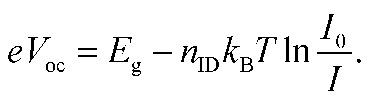
In the following paragraphs we want to briefly review the concept of the diode ideality factor and its relation to charge carrier recombination. From semiconductor theory using the Born–Oppenheimer approximation and Boltzmann statistics, and assuming a perfectly contacted homogeneous absorber with bandgap Eg, Voc can be expressed as:23,24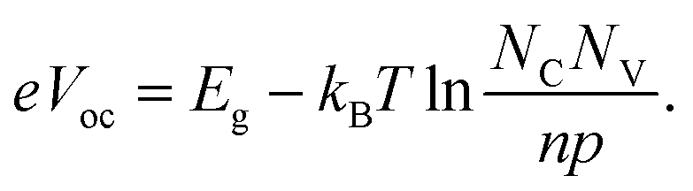 | (1) |
The second term results from the chemical potential of electrons with concentration n and holes (p) partially occupying their effective density of states in the conduction and valance band (NC, NV, respectively). The prefactor of this second term (“thermal voltage” kBT with Boltzmann constant kB) is mainly responsible for the temperature (T) dependence of Voc, whereas n and p result from the equilibrium between optical charge carrier generation G and recombination R, yielding the following equation valid at open circuit:
| G = R(n,p). | (2) |
Here, G is proportional to the light intensity. For the recombination rate as a function of the charge carrier densities we can write dependent on the recombination mechanism:
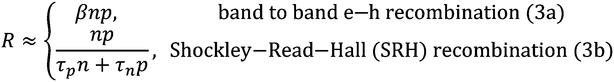 | (3) |
 | (4) |
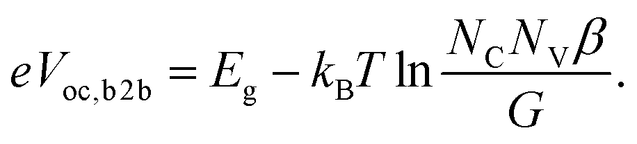
Assuming an intrinsic semiconductor or that n and p are predominantly photogenerated, i.e. n = p, we get for SRH recombination ((3b) in (2) in (1)):
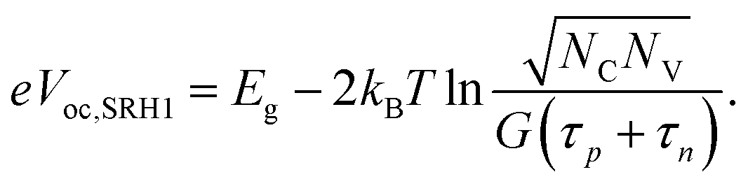 | (5) |
In both cases, Voc depends logarithmically on the light intensity (via G), and we can introduce a prefactor, the so-called diode ideality factor nID, which can be determined from a measurement of Voc as a function of light intensity I:
 | (6) |
Here, I0 is a constant with the same unit as I. In a MIM (metal–intrinsic semiconductor–metal) or p–i–n solar cell with a homogeneous recombination profile in the intrinsic (low-mobility) absorber, the experimentally determined nID can be directly used to identify the dominating recombination mechanism according to eqn (4)–(6).
However, assuming that a high equilibrium of electron (or hole) density exists in the absorber, e.g. introduced by doping, n = p does not hold any more. For a considerably n-doped material, n would equal the concentration of ionized dopants (n ≈ N+D) independent of light intensity. Thus, in this case, photogenerated holes are minorities p ≪ n. Instead of reaching eqn (5), we get:
 | (7) |
The ideality factor is 1 and Voc increases with the doping concentration, because the electron quasi Fermi level is fixed by the large ND. Thus, for a Schottky or pn junction, nID = 1 for recombination in the so-called quasi-neutral region (i.e. N+D = n ≫ p), whereas nID = 2 for recombination in the depletion region. To establish distinct space-charge and quasi-neutral regions in a 500 nm thin perovskite film, (unintentional) high doping densities in the order of 1017 cm−3 would be required. In a MIM device, recombination close to the contacts, where high dark carrier densities prevail, yields nID = 1 as well.
Furthermore, in a real perovskite solar cell, redistribution of photogenerated charges, defect distributions, and recombination at the contacts (which we so far ignored) complicate the situation. R becomes a function of the spatial coordinate x and eqn (2) is not valid any more at each x, but just holds integrated over the absorber thickness.
Fig. 1 gives an overview of how nID depends on recombination processes. Besides the discussed cases, surface recombination due to non-selective contacts is considered as well. It leads to an nID<2 despite SRH recombination and even <1 if Voc is limited by a built-in potential (Vbi, e.g. originating from the difference of work function of the electrodes) and saturates with light intensity once it approaches Vbi because the “driving force” for charge separation vanishes.26 This case of surface recombination is an example for a correlation of Voc and nID that is contrary to common belief. A lower ideality factor is not necessarily beneficial for solar cell performance and can come along with a lower Voc compared to a case where SRH recombination in the bulk limits Voc and nID > 1. This is e.g. observed at perovskite solar cells with an unmodified PEDOT:PSS electrode, where nID = 1, but Voc is low (<1 V).14,27,28
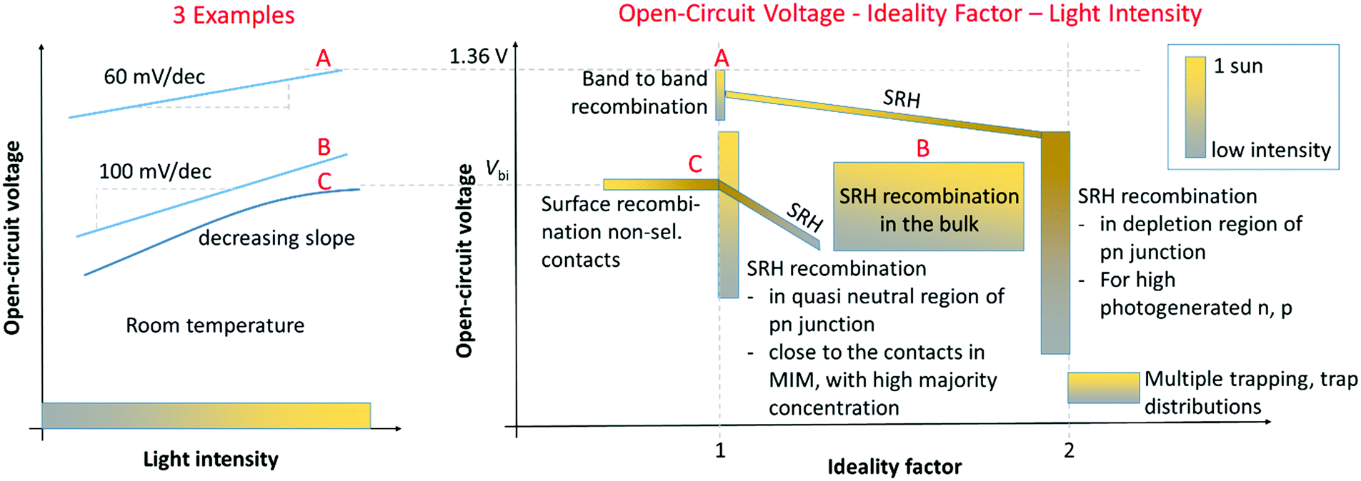 | ||
| Fig. 1 Ideality factor for different recombination mechanisms and corresponding trends in Voc with illumination intensity (gradient). The shaded areas show possible combinations of nID and Voc, where Voc is not to scale. The ideality factor can change with illumination intensity and increase for lower Voc (tilted areas), in particular if radiative or surface recombination appear paired with SRH recombination, with the latter dominating at lower light intensities. However, high Voc is possible for high nID and nID is not a simple quality factor correlated with Voc. SRH recombination can lead to ideality factors between 1 and 2. The left diagram shows three examples, how a measurement of Vocvs. illumination intensity would look like in cases A–C. | ||
Cases with spatially varying R can be treated with numerical drift-diffusion simulations of e.g. a simple MIM architecture. Assuming parameters considered realistic for perovskite solar cells (β = 3 × 10⁻¹¹ cm3 s−1, SRH lifetime 1 μs, mobilities 10 cm2 V−1 s−1),10,14 we get an nID of 1.6. This is because the recombination zone is not limited to a narrow space charge region but extends over the absorber layer. Similar results including those discussed above have been obtained by simulation studies on p–i–n and pn structures.29,30
In a real solar cell, G is not constant either, but a function of x and the wavelength of the light due to thin film optics and a wavelength-dependent absorption coefficient. It seems to have less influence on nID (assuming mobilities of 10 cm2 V−1 s−1) but can be exploited to some extent when explaining changes of Voc and for identifying localized recombination processes in case of imbalanced and/or low mobilities, where recombination happens faster than a redistribution of charges, as reported for meso-TiO2 based10,20 or aged19 devices.
Ideality factor from electroluminescence
Alternatively to using charge carrier densities (eqn (1)), Voc can be derived from a detailed-balance analysis of absorbed and emitted photon flux:31,32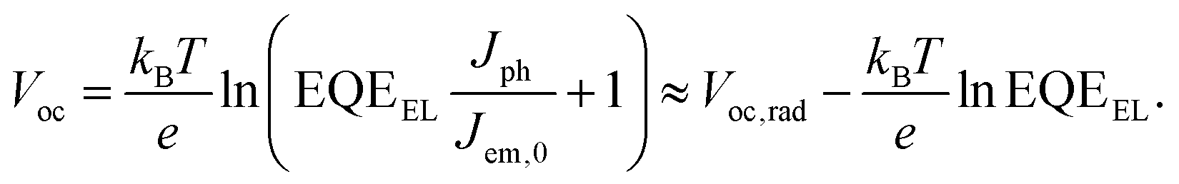 | (8) |
Being consistent with eqn (1), eqn (8) describes the complete device using currents (Jph: photocurrent, Jem,0: dark emission current) instead of local charge carrier densities. The first term Voc,rad describes the radiative limit of Voc, which is 1.33 V for CH3NH3PbI3 with a band gap of around 1.56 eV.33,34 For the mixed cation mixed halide perovskites employed in this work, Voc,rad is 1.36 V, calculated based on the IPCE and the PL spectrum with a maximum at 760 nm (1.62 eV) (Fig. S1, ESI†). The second term of eqn (8) contains a Voc-loss due to non-radiative recombination described by the EQEEL, which is the external quantum efficiency of electroluminescence (EL). Comparing eqn (8) with eqn (6), we see that nID is contained in the EQEEL as a function of illumination intensity: Voc scales with  . Thus, for nID = 1, the EQEEL should be constant, whereas it should increase linearly with light intensity for nID = 2.35,36 Therefore, determining nID from the EQEEL as a function of the injection current, is a complementary way to analyzing Vocvs. light intensity.
Ideality factor from dark JV curve
The EL, which is measured in the dark, links us to a further method employed in this work to determine nID: directly using the JV curve of the diode measured in the dark: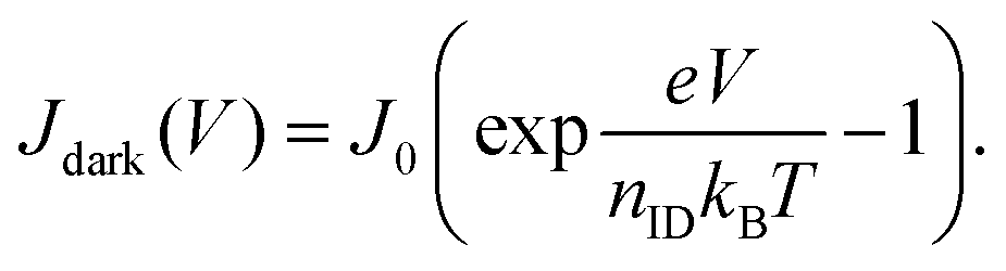 | (9) |
This is the ideal diode equation, which does not take into account parasitic resistances. Here, nID can be determined from the “slope” in the exponential region of a measured JV curve. Determining Voc with the superposition principle (Jdark(Voc) = Jph in eqn (9)), shows that also this equation is consistent with the previous ones.
In summary, the three methods presented should yield the same value for nID if nID can be well-determined and is independent of illumination intensity and applied voltage. In the following, we analyze whether this is the case for experimental data from perovskite solar cells and draw conclusions on dominant recombination mechanisms.
Experimental
The ideality factor is analyzed at state-of-the-art devices (FTO/electron selective contact/perovskite/spiro-MeOTAD/Au) containing ≈500 nm thin mixed ion (“Cs0.05(MA0.17FA0.83)0.95Pb(I0.83Br0.17)3”) perovskite37 absorber layers (optical characterization in Fig. S1, ESI†). Such devices are well-suited for a study of relevant recombination limits, as they can deliver an efficiency >20% and a Voc > 1.2 V.38 The data presented in the following is selected based on results from various measurements on devices containing the following architectures: devices with (i) planar SnO2![[thin space (1/6-em)]](https://www.rsc.org/images/entities/char_2009.gif) 38,39 and (ii) mesoporous (plus compact) TiO2 electron selective layer, both with doped Spiro-MeOTAD as the hole-transport layer (HTL), (iii) aged (8 days under 1 Sun white-light LED illumination at 65 °C in N2) device of the second architecture and (iv) device without the HTL (Fig. 2). Where relevant, data upon light soaking is added to the analysis. Representative JV curves measured under simulated sunlight are shown in Fig. S2 (ESI†) and the characteristic parameters in Table S1 (ESI†).
38,39 and (ii) mesoporous (plus compact) TiO2 electron selective layer, both with doped Spiro-MeOTAD as the hole-transport layer (HTL), (iii) aged (8 days under 1 Sun white-light LED illumination at 65 °C in N2) device of the second architecture and (iv) device without the HTL (Fig. 2). Where relevant, data upon light soaking is added to the analysis. Representative JV curves measured under simulated sunlight are shown in Fig. S2 (ESI†) and the characteristic parameters in Table S1 (ESI†).
 | ||
| Fig. 2 Schematics of investigated devices. Cmp + meso TiO2 stands for a compact and mesoporous TiO2 layer deposited onto fluorine-doped tin oxide (FTO). | ||
Perovskite solar cells are not entirely stable and suffer from reversible and irreversible degradation that can occur during measurements,20,40 in particular when varying temperature.22 Therefore, it is challenging to perform measurements in the time window between ionic response (reversible) and degradation (irreversible).41 In this study reproducibility is guaranteed by repeating measurement series and designing sequences in temperature and intensity containing forward and reverse sweeps. Measurement time is optimized to minimize the effect of slow changes due to light soaking or the application of voltage bias. Therefore, the intensity sweeps are performed rather quickly (3 s settling time, see Fig. S3, ESI†) instead of waiting for minutes for a stabilized Voc, which would result in a reduced Voc in particular at high illumination intensity and temperature, where reversible losses would superimpose the results and reduce reproducibility. Illumination is provided by white LEDs (emission between 400 and 700 nm) and temperature is controlled with a Peltier element. Devices are kept in an airtight chamber under nitrogen flow to avoid irreversible degradation during the measurements. Selected and processed data is used in this work to analyze trends rather than single specific values.
Results
Dark JV curves
To study recombination in the dark, we measured JV curves and extracted nID with the aid of eqn (9) (JV curves under LED illumination in Fig. S4 and S5, ESI†). Fig. 3 shows the JV curves obtained from a voltage loop with a sweep rate of 20 mV s−1 starting at 0 V. All devices show a hysteresis, which mainly affects the shunt regime at low currents. Eqn (9) is valid only in the exponential region (around 1 V), whereas most of the JV curve is dominated by parasitic effects due to shunt and series resistances. Therefore, in line with previous studies42,43 we analyze the phenomenological differential ideality factor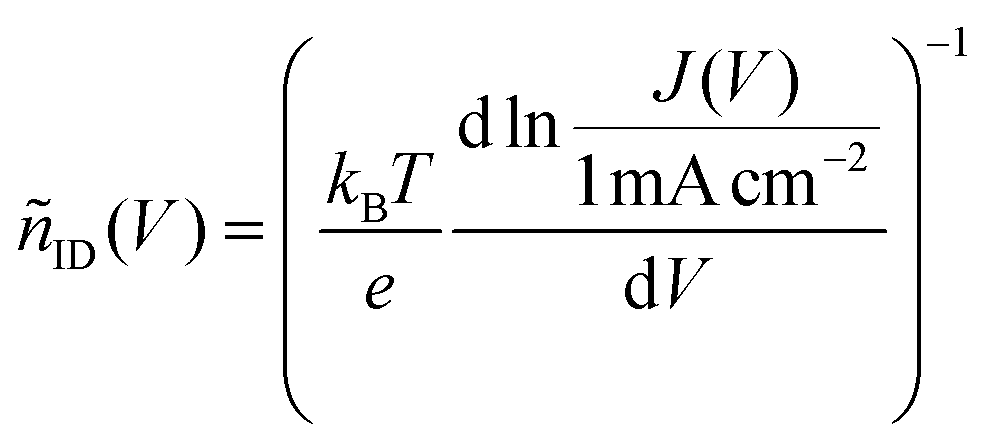 | (10) |
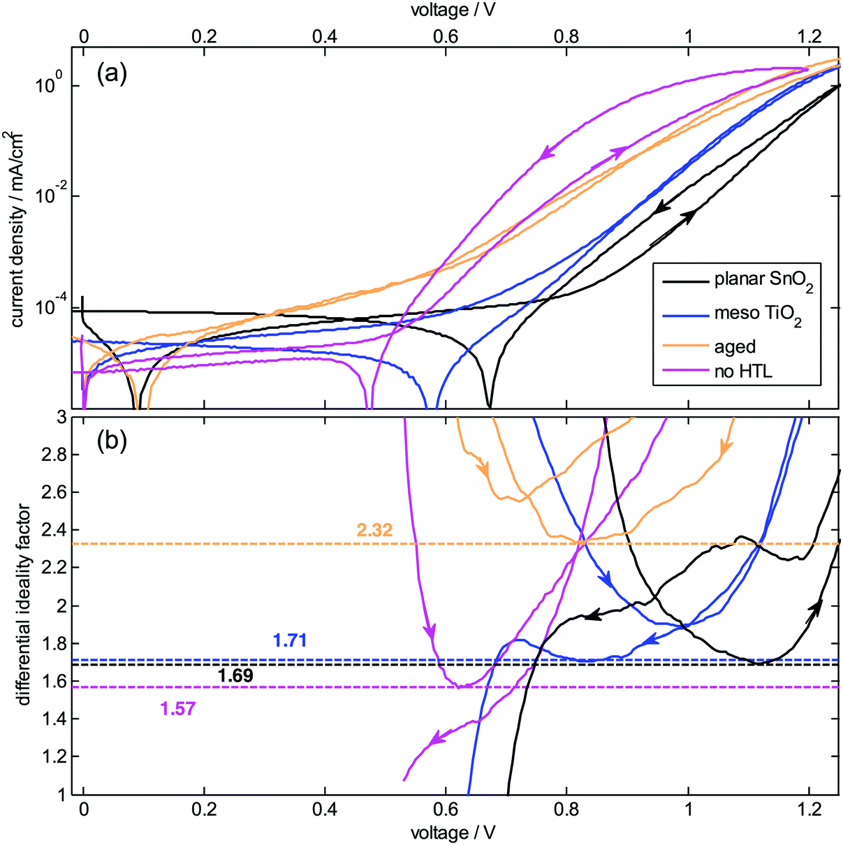 | ||
| Fig. 3 Dark analysis of the diode ideality factor (a) JV curves measured in the dark at 20 °C. (b) Phenomenological differential ideality factor ñID extracted from the differential slope of the JV curves according to eqn (10). Limitations by resistances render this approach unreliable for the investigated perovskite solar cells. | ||
Light intensity dependent Voc
The limitations by the series resistance can be completely overcome when analyzing Vocvs. illumination intensity, as the net current is 0 at Voc, and thus voltage is not lost due to the series resistance. Fig. 4 shows Voc as a function of illumination intensity in an intensity range covering four orders of magnitude and during a sweep from dark conditions to 1.5 Suns equivalents (“upward”, open symbols in Fig. 4) and back (“downward”, closed symbols). The data is extracted as shown in Fig. S3 (ESI†). The Voc at 1 Sun is ≈1.2 V for the fresh devices, whereas the aged device shows a Voc of 1 V and the one without HTL of 0.8 V. All traces look approximately linear in this plot and limitations by a too low shunt resistance (as often observable) are visible only in the aged device at low light intensity (which is not necessarily due to the fact that it was aged but due to device-to-device variations). Despite the linear appearance, it is advisable to perform a differential analysis36,44 of the slope here as well and deduce a phenomenological ideality factor analogously to eqn (10): | (11) |
 | ||
| Fig. 4 The diode ideality factor from light-intensity dependent open-circuit voltage analysis at 20 °C. Data obtained in “upward” (open) and subsequent “downward” (closed symbols) intensity sweep with 3 s settling time at each light intensity. (a) Vocvs. light intensity, where dashed lines show a logarithmic fit and the numbers indicate nID deduced from the slope. (b) Phenomenological ideality factor extracted from the slope of the data in (a) according to eqn (11). The numbers give an estimate of an intrinsic nID obtained from the intermediate intensity regime. At higher intensities, surface recombination leads to a reduction of nID. | ||
This data is plotted in Fig. 4b and reveals that the slope is not perfectly constant but shows several trends. It increases for the upward trace for all devices toward low light intensity due to the measurement procedure and an observed slow response of a device after it has been kept in the dark, which is consistent with observations of hysteresis in perovskite solar cells.41,45,46 For the aged device it increases also for the downward trace (closed symbols) because of the already mentioned shunt. Therefore, this low-intensity part of the data is not to be further analyzed. Most of the traces show a constant phenomenological nID* at intermediate light intensity (10−3–10−1 Suns), which justifies attribution to an intrinsic nID in eqn (6). It is between 1.6 and 1.7 for the planar device (the 2 directions deliver slightly different values), around 1.8 for the meso device, 2 for the aged device, and 1.3 for the device without HTL. In the cases here, these values roughly coincide with an ideality factor extracted from a logarithmic fit of the overall data (dashed lines and numbers in Fig. 4a). They also follow the trends deduced from the dark JV curves, but are slightly lower and more reliable because the series resistance effects are avoided, as also found for organic solar cells.36
The ideality factor hardly depends on the electron selective layer (SnO2vs. TiO2) or the planar or mesoscopic nature of the electron contact indicating that charge recombination is not dominated by these interfaces. Interestingly, nID tends to decrease for higher illumination intensities, in particular for the aged and the HTL-free device where it approaches 1 indicative of surface recombination setting in for higher Voc (cf.Fig. 1).26 The dependence of nID* on light intensity (and therefore on voltage) also explains potentially observed discrepancies between nID obtained from JV curves and from Vocvs. light intensity around 1 Sun, because the latter is measured at higher voltages. Real differences between both methods, which would indicate different recombination mechanisms, might be possible if poor conductivities cause large gradients in quasi-Fermi levels at Voc. Further interpretations of the data will be given in the discussion section.
Temperature dependent nID
To reliably identify nID, it is important to perform measurements at different temperatures because nID appears paired with the thermal energy kBT in the presented equations. Therefore, the above analyses on the dark JV curves and the Vocvs. light intensity plots were repeated at different temperatures, starting at 20 °C, followed by a decrease to −10 °C, a rise to 50 °C (in steps of 10 K) and completed at 20 °C. The obtained values for the phenomenological nID are summarized in Fig. 5. If the measured slopes were independent of temperature, the deduced nID would follow the black dotted line. In that case, an interpretation of the measurement results at room temperature using nID and above equations would not be meaningful. However, for most of the measurements the deduced nID seems rather independent of temperature in the measured range and fluctuations are within the experimental error, which is already significant considering the dependence of nID* on light intensity (cf.Fig. 4b). Nevertheless, the major conclusions are solid: consistent with the room temperature analysis, the planar device exhibits an average ideality factor derived from the different techniques between 1.6 and 1.8 (Fig. 5a) (JV backward scan is an exception), similar to the mesoporous TiO2 device (Fig. 5b). Interestingly the backward JV scan of the planar device and the forward JV scan for the meso device result in values larger than 2 indicative of a hysteresis-induced change of recombination mechanism towards a regime observed at the aged device, which shows an ideality factor close to 2 also when deduced from the Voc (Fig. 5c). On the other hand, resistive effects caused by ion-induced changes in charge injection rate, might be responsible for this observation, which is not seen for every device (cf.Fig. 6c). For the device without HTL, the previously observed low nID between 1.1 and 1.3 is confirmed by the temperature dependent Voc (Fig. 5d). The strong temperature dependence of nID obtained from the JV curve of this device without HTL is due to a strong increase of series resistance when decreasing T, as already indicative by the JV curves measured at 20 °C (cf.Fig. 3) and does therefore not describe the real nID. In general, nID obtained from the JV curves is less reproducible compared to the Vocvs. light intensity method.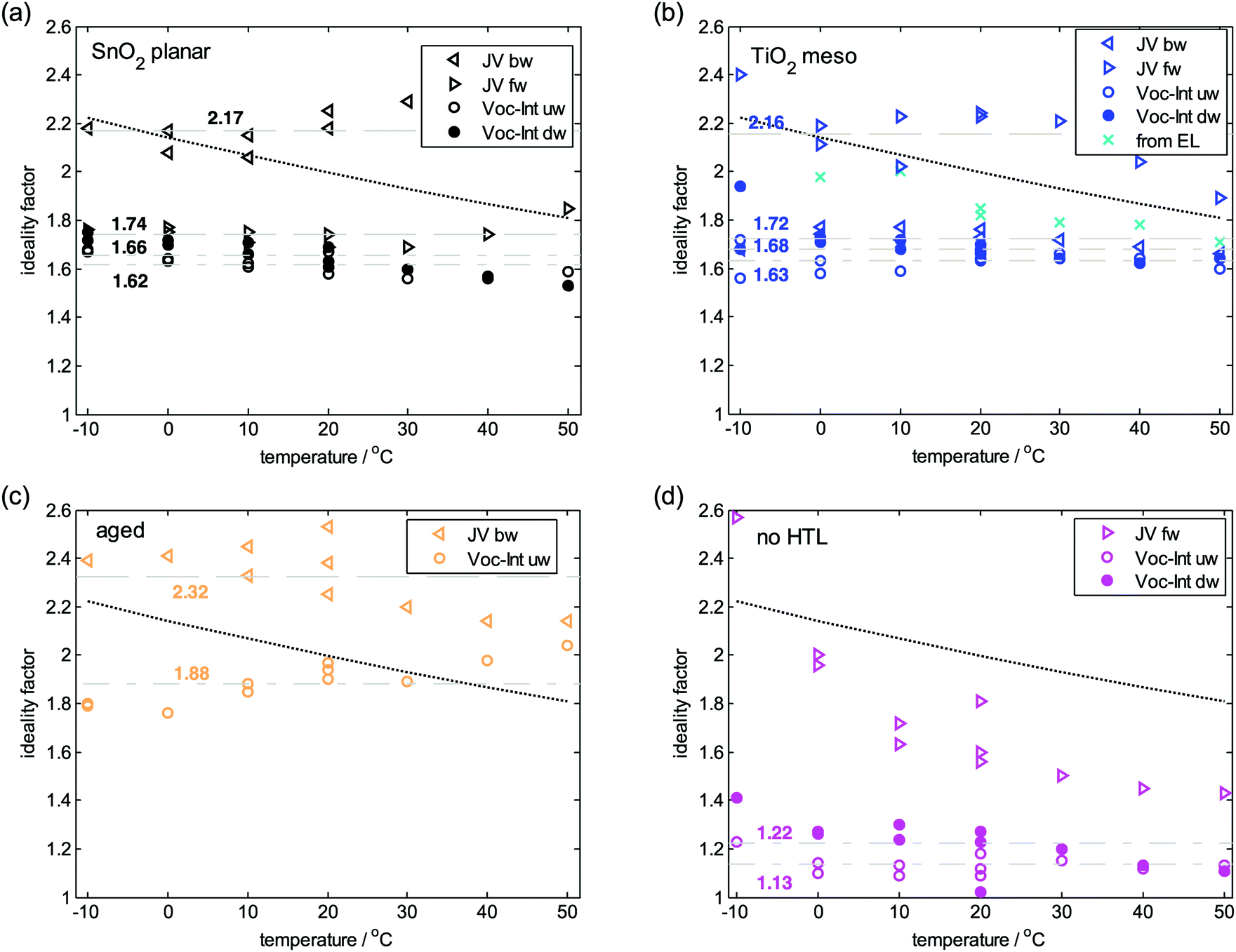 | ||
| Fig. 5 The ideality factor from forward (fw) and backward (bw) scan JV curves and from Vocvs. light intensity data in upward (uw) and downward (dw) trace. The dashed lines paired with the displayed number denote the mean value. If data traces are missing, it would have been too arbitrary to extract an ideality factor from the experimental data. The black dotted line represents the trend expected in case of slopes in eqn (9) and (10) independent of temperature resulting into an apparent dependence of the ideality factor on temperature. Values extracted from JV curves are affected by hysteresis and less reliable compared to those from Vocvs. light intensity. | ||
 | ||
| Fig. 6 Temperature dependent electroluminescence of meso-TiO2 (a and b) and planar SnO2 (c–f) device. (a) EQEEL as a function of the injection current obtained during a forward voltage sweep followed by a backward sweep. EQEEL of an HTM-free device recorded at 25 °C is added (magenta, right axis), yielding an ideality factor of ≈1.3. (b) Emitted photon flux for a constant current of 0.1 mA applied for 1 minute starting at 10 s. (c) Dark JV curves at different temperatures, (d) extracted differential ideality factor from dark JV curves, (e) extracted differential ideality factor from EQEEL, (f) comparison of ideality factors as a function of temperature. | ||
Ideality factor from electroluminescence
For the meso-TiO2 device, nID obtained from temperature dependent EL measurements (eqn (8)) is added to Fig. 5b as well, resulting in values between 1.7 and 2. They have been extracted from the data in Fig. 6, showing the EQEEL as a function of the injection current in a double logarithmic scale. The EQEEL and its “slope” are rather independent of temperature as expected for an unmodified nID. However, a strong hysteresis occurs at elevated temperatures, where the EQEEL undergoes a considerable reduction while applying currents larger than 0.1 mA, resulting in an order of magnitude lower values in the backward scan. This instability is seen in Fig. 6b as well, where the photon flux is monitored at a constant injection current of 0.1 mA, leading to a rapid decay of the EL signal for T > 40 °C. The final measurement at 20 °C (dash-dotted) shows that this decrease is reversible. The rise time of the EL after applying the constant current decreases with T, indicating that a certain ion displacement is required to reach the highest share of radiative recombination.41 This could have several reasons, e.g. related to a more balanced injection of electrons and holes upon ion accumulation or the removal of non-radiative recombination centers in the perovskite film. Whereas this transient behavior remains subject for further studies, the stabilized EL is of importance in the context of this study. We observe that the stabilized EL value does not depend on the temperature in the investigated T range, which is a requirement to apply aforementioned equations to describe Voc and proceed with the following analysis. The main advantage of this method against the dark JV analysis is its independence of series resistance as the EQEEL is analyzed as a function of the current (instead of voltage). A device without HTL (magenta in Fig. 6a) shows low EQEEL as expected from eqn (8) and the deduced ideality factor is ≈1.3 consistent with the other data. Fig. 6c–f show a detailed example on a planar device, where ideality factors between 1.5 and 1.7 are deduced from JV curves and EL.Activation energy of recombination from temperature dependent Voc
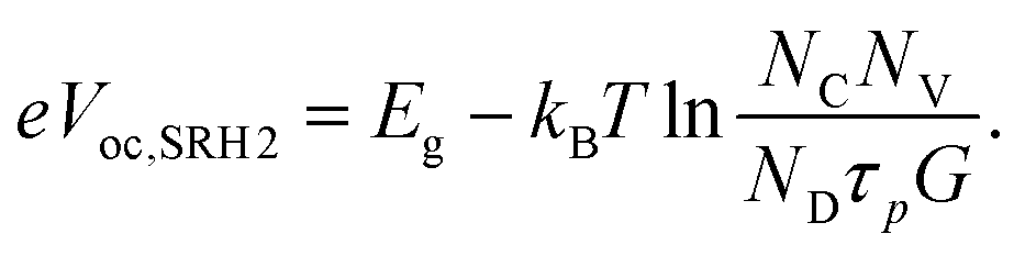
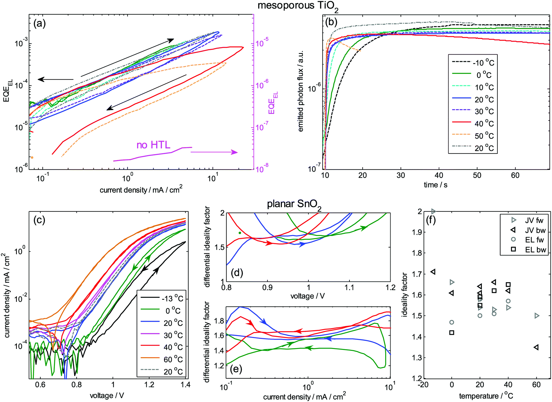
We plot Voc as a function of temperature for different illumination intensities and compare the traces with the prediction from eqn (1). This equation predicts that Voc should be linear in T and reach Eg/e independent of illumination intensity when extrapolated for T → 0 K. The planar device in Fig. 7a seems to follow this linear trend, with extrapolated values between 1.5 and 1.6 V. It has to be noted that the extrapolation from values close to room temperature introduces a considerable uncertainty and accuracy is not expected to reach values smaller than ±0.1 V in our experiment. The meso-TiO2 device (Fig. 7b) shows less clear linear dependence in particular at higher light intensities, which can be partially explained by a fast reversible decrease of Voc at elevated T, already during the measurement (cf. Fig. S7, ESI†). Nevertheless, the linear extrapolation yields values close to Eg/e, but a bit lower in particular for lower light intensities. This could indicate partially filled trap states at the TiO2, an effect that is more pronounced for low-Voc devices.47 In contrast, the degraded device (Fig. 7c), which has 0.2 V lower Voc at 20 °C and 1 Sun, exhibits decreasing values for T → 0 K with increased light intensity. As the linear trend seems still observable, we can fit the data with a linear function but introducing a general activation energy of recombination, Ea, (as e.g. done in ref. 48) that replaces Eg and will be discussed later: | (12) |
 | ||
| Fig. 7 Temperature dependence of Voc and light soaking. (a–d) Vocvs. T for different light intensities and linear fits yielding an activation energy Ea for T → 0 K. (In case of b, for 1 and 0.1 Sun, T > 30 °C have been ignored for the fit, see Fig. S7 (ESI†); in c, values below 0 °C have been ignored due to too slow response; in d different regimes are observed for 1 and 0.1 Sun indicated by fitting two lines.) (e) Vocvs. T at 1 Sun for all devices investigated (f) transient Voc during light soaking (g) Vocvs. light intensity before and after light soaking. During the recovery period, the devices were kept in the dark for 2 hours. | ||
E a is around 1.4 eV for the aged device and decreases for higher light intensity where Voc seems to saturate. The device without HTL (Fig. 7d) shows an Ea of around 1 eV, which is significantly lower than the actual Eg. The two lines for the higher intensity visualize that fitting a single linear function becomes more difficult in this regime. For a better comparability, the data for 1 Sun illumination of all devices is summarized in Fig. 7e, showing that the planar and meso devices are limited by bulk recombination.
Light-soaking
We now investigate the devices after they have been exposed to 1 Sun (LED equivalent) illumination for 80 minutes at open circuit (“light soaking”). The transients of Voc are monitored and plotted in Fig. 7f showing a strong decrease of Voc for the meso-TiO2 and planar device, whereas Voc of the aged devices changes less and even improves for early times. Directly after 80 minutes of light soaking the temperature dependence of Voc at 1 Sun was recorded which is added to the graphs in Fig. 7a–c (circles). Fitting with eqn (9) yields an Ea of around 1.3 to 1.4 eV, much lower than Ea for meso-TiO2 and planar devices, but slightly larger than for the aged device. These data is added as dash-dotted lines to Fig. 7e as well. The light soaking effect is reversible as shown by Vocvs. light intensity data collected at 20 °C before light soaking and after recovery, which are almost identical (Fig. 5g).Discussion
We now want to interpret the obtained results for nID and Ea to better understand recombination for the different devices. We start with Ea. An Ea < Eg is commonly attributed to recombination of charge carriers that do not reside at the band edges of the absorber, but e.g. at interfaces of heterojunctions or surfaces (Fig. 8). This is because the potential energy of electron–hole pairs recombining through a heterojunction interface can be lower than Eg of the absorber due to a lower (higher) conduction (valence) band edge of the adjacent material. Furthermore, tail states and non-selective contacts can lead to a reduced Ea as illustrated in Fig. 8. | ||
| Fig. 8 Illustration of the value of Ea (in eqn (12)) dependent on the recombination process. Blue are conduction and valence band edge of the absorber (perovskite). An Ea < Eg is due to recombination at heterojunctions, surfaces or via tail states. | ||
To determine whether such states with energies below Eg exist, sensitive measurements of the incident-photon-to-current-efficiency (IPCE) onset were carried out using Fourier Transform Photocurrent Spectroscopy (FTPS). Fig. 9a shows data for the light-soaking experiment performed at a meso TiO2 device. The band gap at around 1.6 eV and the Urbach energy of around 15 meV remain unchanged upon light soaking. However, a new feature appears (or becomes more pronounced) with a peak at 1.35 eV extending towards 1.1 eV. It is strongest directly after the light soaking and tends to disappear after a recovery period in the dark. Interestingly, the energy of this feature coincides with Ea obtained from the temperature dependent measurements after light soaking (Fig. 7d). Therefore, we conclude that the reduced Voc after light soaking is due to a reversible photoinduced formation of defect states, which open up new recombination channels. Observing that this happens in all investigated architectures independent of the contacts, corroborated also by the Vocvs. time in Fig. 7f, we attribute it to photogenerated defects in the perovskite. It seems as these defects form during the reversible degradation upon light exposure as hypothesized in ref. 49, where surprisingly Voc showed the opposite trend. However, in a control experiment, light-soaked films do not show increased PL quenching compared to films kept in the dark under N2 atmosphere (Fig. S8 and S9, ESI†), confirming that the perovskite composition is photostable. In some samples the PL rather slightly increases consistent with what is commonly seen in PL studies,50 but in contrast to a recent study, where a reduced PL yield and emission from subgap states have been reported after illumination.51 The photobrightening has been attributed to a photoinduced halide redistribution, decreasing the density of bulk defects.52 Therefore, to explain our Voc decrease, we rule out a solely photoinduced defect formation in the bulk of the perovskite. Instead the defects might become active at an interface and could be indeed mobile ions, e.g.,52 I− that lead to the reversible photo degradation.40 Repeating the lightsoaking PL study on films deposited on FTO/TiO2, we see a similar trend as on glass (Fig. S10, ESI†). In contrast, on complete devices the PL yield is indeed decreased after lightsoaking (Fig. S11, ESI†) providing strong evidence that interfaces to charge transport layers (such as HTL) play a crucial role. A similar effect on Voc has been reported very recently and attributed to enhanced interfacial recombination at the TiO2 interface due to an accumulation of cations and holes leading to increased surface recombination.21 The importance of changes in surface recombination during light-soaking are also evident at (inverted) devices with initially very low Voc, where suppressed surface recombination upon ion migration leads to the opposite effect, i.e. an increase of Voc.53 In our study, we do not have the means to identify the interface (ETL or HTL) but note that we observe the same behavior at planar SnO2 based devices yielding the same Ea despite the different energetics expected at the SnO2 interface.39 Even the IPCE of the non-light soaked device seems to show a weak response around 1.35 eV, indicating that the high Voc in pristine devices might still be limited by this feature. It could also be a reason why the Voc of pristine devices shows variations from batch to batch. This hypothesis is consistent with results from admittance spectroscopy on CH3NH3PbI3 perovskite solar cells, where a trap state was found 0.28 eV below the band-gap energy dependent on processing conditions and correlated with hysteresis.54
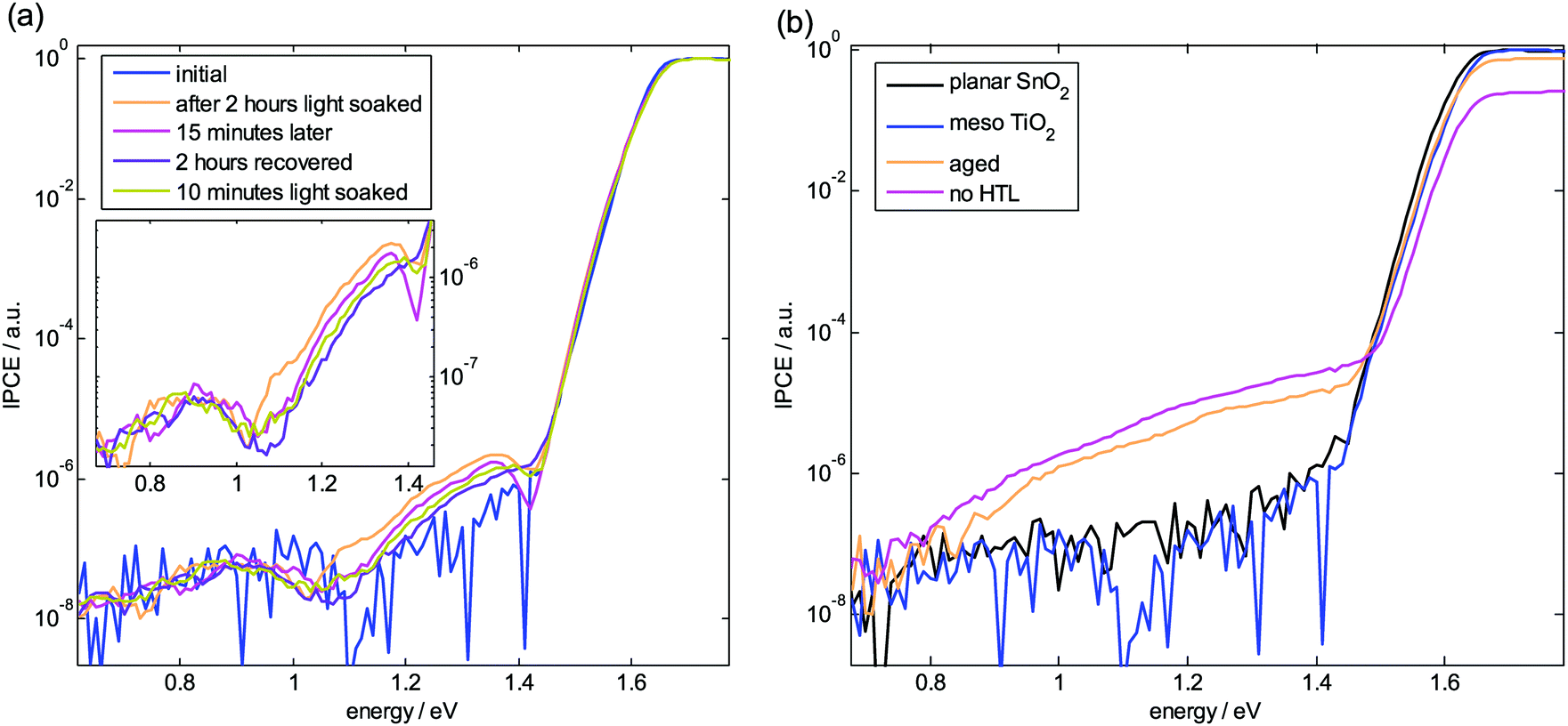 | ||
| Fig. 9 Subgap states from IPCE onset collected by FTPS measurements. (a) Light-soaking of a meso TiO2 device leading to a subgap state at 1.35 eV. (b) Comparison of different devices. | ||
The FTPS spectra in Fig. 9a show an additional feature located at 0.9 eV, whose values are close to the resolution limit of our measurement, but observed in all kinds of devices. This feature needs further investigation but could be a deep trap state which is responsible for the SRH recombination leading to nID > 1. Comparing to calculations of intrinsic point defects, the light-induced defect could result from iodine interstitials as already mentioned, whereas the deep trap could be due to antisites55,56 such as PbI, IPb, which show high formation energies and are therefore expected to be permanent and mainly generated during film formation. On the other hand, impurities could cause such deep trap states as well.57 Signatures of both features58 and deep traps59,60 in CH3NH3PbI3 perovskite solar cells have been identified with other techniques as well, showing that they are not specific to the mixed perovskite composition used in our work.
The Ea of the device without HTL is lowest and seems to increase with light intensity (Fig. 7d). We analyze FTPS data of this device (Fig. 6b) and observe a very broad distribution of subgap states which can explain the low and non-constant Ea. A similar distribution has been reported at low-performance devices, where a correlation between Voc and hysteresis was found.61 Here, we have evidence that these defects are introduced by the direct contact of Au and the perovskite, which is consistent with the extremely pronounced tail reported for planar devices where Au is used for both electrodes.62 The low values of nID indicate that these defects are mainly localized close to the interface to the Au, where we expect a high hole density (cf.Fig. 1). Interestingly the aged device shows the same tail feature as well confirming that Au migrates during degradation, as has already been shown by ToF-SIMS measurements.22 However, for the aged device, nID is around 2 and Ea higher for low light intensities, indicating that SRH recombination through deep defects is responsible for the lower Voc compared to a pristine device. To exclude that recombination centers are generated in the perovskite film itself by the elevated temperatures, we kept films at 65 °C for the same time in an N2 glove box and could not observe a decrease of the PL yield, but rather a small increase, possibly due to an annealing effect (Fig. S12, ESI†). Therefore, it is most likely that the Au, which is more distributed in the perovskite layer, is responsible for recombination in a depletion region. For higher illumination intensities, the limit by surface recombination becomes visible for the aged device as nID decreases towards 1 (Fig. 4) and Ea towards values similar to those of the device without HTL (Fig. 7c). Consistent with the tail states in Fig. 9b, we find an increased doping density in a Mott–Schottky analysis when going from a pristine device to a degraded one to a device without HTL (Fig. S13, ESI†).
Now we shift focus to the pristine devices with high Voc to understand which recombination mechanism has to be addressed to further improve these devices. First, the similar behavior between planar SnO2 and meso-TiO2 based devices lets us conclude that Voc around 1 Sun is not limited by the electron selective layer despite the fact that most of the light is absorbed in its vicinity. This finding confirms the results from our16 and others'19,47 previous studies, but is in contradiction to a recent impedance study, which is interpreted by recombination at the electron selective contact with time constants in the order of 1 s.18 According to Fig. 1 and 8, an nID between 1.5 and 2 and an Ea = Eg is attributed to SRH recombination in the bulk of a mostly intrinsic or depleted perovskite film. This interpretation is consistent with reported PL analyses50 and enforced by the fact that nID does not change over orders of magnitude of illumination intensity, which excludes that the dominant recombination mechanism changes or that the influence of radiative recombination is already visible in nID. As the characteristics of this recombination mechanism are different from the case of light-soaking, we speculate that it is less likely related to intrinsic point defects which are mobile and might be formed by a light-assisted process. One candidate for these permanent recombination centers might be grain boundaries that give rise to defect states. However, experimental data on the perovskite material employed in this study, does not give clear indications that grain boundaries affect Voc at 1 Sun.16 Furthermore, a recent PL mapping study collected evidence for benign grain boundaries63 in contrast to a former PL study,64 which might be explained by different processing conditions and material compositions leading to modified surface termination.65
Another explanation might be related to the FTPS signal at 0.9 eV, which could result from a well-defined recombination center introduced by an antisite defect or an impurity as discussed above. Potential fluctuations due to surface or grain boundary states might be expected to follow a much broader distribution and rather causing an exponential tail in the FTPS instead of a distinct state, as observed for polycrystalline silicon.66 We measured devices with smaller grain size16 as well, which did not show a more pronounced feature in the FTPS spectrum. Therefore, we conclude that whereas low-performance devices with unoptimized perovskite films are most likely limited by recombination at surfaces (interfaces and grain boundaries), the search for recombination centers in the best perovskite solar cells should not be performed ignoring the bulk. More detailed and sophisticated studies will be required to identify the nature of the recombination centers, not only focusing on intrinsic point defects but other intrinsic and extrinsic defects as well, such as impurities.
Conclusions
We have studied recombination in perovskite solar cells employing temperature dependent measurements to determine ideality factor and activation energy, which characterize the predominant recombination process. In doing so, we compared the ideality factor from light-intensity dependent Voc, dark JV, and electroluminescence measurements, which yielded similar values. However, parasitic resistances hamper an unambiguous determination of the ideality factor from JV curves. Therefore, light-intensity dependent Voc is a more reliable method, which is additionally able to resolve changes of recombination regime dependent on charge carrier densities and voltage.We have investigated different devices (Fig. 10) including planar and mesoporous architectures and found that recombination is not severely affected by the n-type contact. On the other hand, devices without hole-transport layer clearly showed the signature of surface recombination. Degraded devices suffered from high defect-recombination, most likely induced by gold migrating into the perovskite. FTPS measurements indicated that Au in contact with perovskite causes a broad distribution of intragap states. In contrast, devices exposed to light-soaking showed a reversible formation of a narrow defect state situated 0.25 eV below the band gap which acts as dominant recombination center.
 | ||
| Fig. 10 Summary of the conclusions. | ||
For pristine optimized devices with Voc of around 1.2 V, an ideality factor of ≈1.6 and the band gap energy as activation energy for recombination indicate that recombination happens in a rather intrinsic/depleted bulk of the absorber layer. Therefore, a further optimization of perovskite solar cells needs to focus on identifying and eliminating defect states in the perovskite film including those of intrinsic and extrinsic nature. This requires a shift of focus in the perovskite solar cell research from compositional and morphology engineering towards identification and characterization of defects and impurities in the ppm regime.
Author contributions
WT designed the study, performed the experiments, analyzed the data and wrote the paper. KD did additional temperature dependent JV measurements. MY and J-P C-B prepared solar cells. BN performed FTPS measurements with WT. PY performed impedance measurements and together with J-P C-B contributed to detailed discussions. AH and MG supervised the students. All authors contributed to the final version of the manuscript.Conflicts of interest
The authors declare no competing financial interests.Acknowledgements
WT acknowledges funding by the Swiss National Science Foundation under an Ambizione Energy grant and MG the King Abdulaziz City for Science and Technology (KACST) for financial support under a joint research project. This work was partially funded by the Nano-Tera.ch “Synergy” project, the Swiss Federal Office of Energy under Grant SI/501072-01, and the Swiss National Science Foundation via the NRP70 “Energy Turnaround” project “PV2050”. We thank our technical staff in particular Benjamin Le Geyt for the excellent collaborative support.References
- W. S. Yang, B.-W. Park, E. H. Jung, N. J. Jeon, Y. C. Kim, D. U. Lee, S. S. Shin, J. Seo, E. K. Kim, J. H. Noh and S. I. Seok, Iodide management in formamidinium-lead-halide–based perovskite layers for efficient solar cells, Science, 2017, 356, 1376–1379 CrossRef CAS PubMed.
- G. E. Eperon, T. Leijtens, K. A. Bush, R. Prasanna, T. Green, J. T.-W. Wang, D. P. McMeekin, G. Volonakis, R. L. Milot, R. May, A. Palmstrom, D. J. Slotcavage, R. A. Belisle, J. B. Patel, E. S. Parrott, R. J. Sutton, W. Ma, F. Moghadam, B. Conings, A. Babayigit, H.-G. Boyen, S. Bent, F. Giustino, L. M. Herz, M. B. Johnston, M. D. McGehee and H. J. Snaith, Perovskite-perovskite tandem photovoltaics with optimized band gaps, Science, 2016, 354, 861–865 CrossRef CAS PubMed.
- J. Werner, L. Barraud, A. Walter, M. Bräuninger, F. Sahli, D. Sacchetto, N. Tétreault, B. Paviet-Salomon, S.-J. Moon, C. Allebé, M. Despeisse, S. Nicolay, S. De Wolf, B. Niesen and C. Ballif, Efficient Near-Infrared-Transparent Perovskite Solar Cells Enabling Direct Comparison of 4-Terminal and Monolithic Perovskite/Silicon Tandem Cells, ACS Energy Lett., 2016, 1, 474–480 CrossRef CAS.
- M. Hirasawa, T. Ishihara and T. Goto, Exciton Features in 0-, 2-, and 3-Dimensional Networks of [PbI6]4- Octahedra, J. Phys. Soc. Jpn., 1994, 63, 3870–3879 CrossRef CAS.
- S. De Wolf, J. Holovsky, S.-J. Moon, P. Löper, B. Niesen, M. Ledinsky, F.-J. Haug, J.-H. Yum and C. Ballif, Organometallic Halide Perovskites: Sharp Optical Absorption Edge and Its Relation to Photovoltaic Performance, J. Phys. Chem. Lett., 2014, 5, 1035–1039 CrossRef CAS PubMed.
- W. Shockley and H. J. Queisser, Detailed Balance Limit of Efficiency of p-n Junction Solar Cells, J. Appl. Phys., 1961, 32, 510–519 CrossRef CAS.
- C. Wehrenfennig, G. E. Eperon, M. B. Johnston and H. J. Snaith, & Herz, L. M. High Charge Carrier Mobilities and Lifetimes in Organolead Trihalide Perovskites, Adv. Mater., 2014, 26, 1584–1589 CrossRef CAS PubMed.
- G. Xing, N. Mathews, S. Sun, S. S. Lim, Y. M. Lam, M. Grätzel, S. Mhaisalkar and T. C. Sum, Long-Range Balanced Electron- and Hole-Transport Lengths in Organic-Inorganic CH3NH3PbI3, Science, 2013, 342, 344–347 CrossRef CAS PubMed.
- S. D. Stranks, G. E. Eperon, G. Grancini, C. Menelaou, M. J. P. Alcocer, T. Leijtens, L. M. Herz, A. Petrozza and H. J. Snaith, Electron–Hole Diffusion Lengths Exceeding 1 Micrometer in an Organometal Trihalide Perovskite Absorber, Science, 2013, 342, 341–344 CrossRef CAS PubMed.
- D. Bi, W. Tress, M. I. Dar, P. Gao, J. Luo, C. Renevier, K. Schenk, A. Abate, F. Giordano, J.-P. C. Baena, J.-D. Decoppet, S. M. Zakeeruddin, M. K. Nazeeruddin, M. Grätzel and A. Hagfeldt, Efficient luminescent solar cells based on tailored mixed-cation perovskites, Sci. Adv., 2016, 2, e1501170 Search PubMed.
- M. Saliba, T. Matsui, K. Domanski, J.-Y. Seo, A. Ummadisingu, S. M. Zakeeruddin, J.-P. Correa-Baena, W. R. Tress, A. Abate, A. Hagfeldt and M. Grätzel, Incorporation of rubidium cations into perovskite solar cells improves photovoltaic performance, Science, 2016, 354, 206–209 CrossRef CAS PubMed.
- W.-J. Yin, T. Shi and Y. Yan, Unusual defect physics in CH3NH3PbI3 perovskite solar cell absorber, Appl. Phys. Lett., 2014, 104, 063903 CrossRef.
- J. Kim, S.-H. Lee, J. H. Lee and K.-H. Hong, The Role of Intrinsic Defects in Methylammonium Lead Iodide Perovskite, J. Phys. Chem. Lett., 2014, 5, 1312–1317 CrossRef CAS PubMed.
- W. Perovskite Solar Tress, Cells on the Way to Their Radiative Efficiency Limit – Insights Into a Success Story of High Open-Circuit Voltage and Low Recombination, Adv. Energy Mater., 2017, 7, 1602358 CrossRef.
- J.-P. Correa-Baena, M. Anaya, G. Lozano, W. Tress, K. Domanski, M. Saliba, T. Matsui, T. J. Jacobsson, M. E. Calvo, A. Abate, M. Grätzel, H. Míguez and A. Hagfeldt, Unbroken Perovskite: Interplay of Morphology, Electro-optical Properties, and Ionic Movement, Adv. Mater., 2016, 28, 5031–5037 CrossRef CAS PubMed.
- J.-P. Correa-Baena, W. Tress, K. Domanski, E. H. Anaraki, S.-H. Turren-Cruz, B. Roose, P. P. Boix, M. Grätzel, M. Saliba, A. Abate and A. Hagfeldt, Identifying and suppressing interfacial recombination to achieve high open-circuit voltage in perovskite solar cells, Energy Environ. Sci., 2017, 10, 1207–1212 CAS.
- J.-P. Correa-Baena, S.-H. Turren-Cruz, W. Tress, A. Hagfeldt, C. Aranda, L. Shooshtari, J. Bisquert and A. Guerrero, Changes from Bulk to Surface Recombination Mechanisms between Pristine and Cycled Perovskite Solar Cells, ACS Energy Lett., 2017, 2, 681–688 CrossRef CAS.
- I. Zarazua, G. Han, P. P. Boix, S. Mhaisalkar, F. Fabregat-Santiago, I. Mora-Seró, J. Bisquert and G. Garcia-Belmonte, Surface Recombination and Collection Efficiency in Perovskite Solar Cells from Impedance Analysis, J. Phys. Chem. Lett., 2016, 7, 5105–5113 CrossRef CAS PubMed.
- L. Contreras-Bernal, M. Salado, A. Todinova, L. Calio, S. Ahmad, J. Idígoras and J. A. Anta, Origin and Whereabouts of Recombination in Perovskite Solar Cells, J. Phys. Chem. C, 2017, 121, 9705–9713 CAS.
- W. Tress, J. P. Correa Baena, M. Saliba, A. Abate and M. Graetzel, Inverted Current–Voltage Hysteresis in Mixed Perovskite Solar Cells: Polarization, Energy Barriers, and Defect Recombination, Adv. Energy Mater., 2016, 6, 1600396 CrossRef.
- J. Hu, R. Gottesman, L. Gouda, A. Kama, M. Priel, S. Tirosh, J. Bisquert and A. Zaban, Photovoltage Behavior in Perovskite Solar Cells under Light-Soaking Showing Photoinduced Interfacial Changes, ACS Energy Lett., 2017, 2, 950–956 CrossRef.
- K. Domanski, J.-P. Correa-Baena, N. Mine, M. K. Nazeeruddin, A. Abate, M. Saliba, W. Tress, A. Hagfeldt and M. Grätzel, Not All That Glitters Is Gold: Metal-Migration-Induced Degradation in Perovskite Solar Cells, ACS Nano, 2016, 10, 6306–6314 CrossRef CAS PubMed.
- W. Tress, Organic Solar Cells – Theory, Experiment, and Device Simulation, at http://www.springer.com/materials/optical+%26+electronic+materials/book/978-3-319-10096-8.
- W. Tress, Organic–Inorganic Halide Perovskite Photovoltaics, Springer, Cham, 2016, pp. 53–77 DOI:10.1007/978-3-319-35114-8_3.
- W. Shockley and W. T. Read, Statistics of the Recombinations of Holes and Electrons, Phys. Rev., 1952, 87, 835–842 CrossRef CAS.
- W. Tress, K. Leo and M. Riede, Dominating recombination mechanisms in organic solar cells based on ZnPc and C60, Appl. Phys. Lett., 2013, 102, 163901 CrossRef.
- K. Miyano, M. Yanagida, N. Tripathi and Y. Shirai, Simple characterization of electronic processes in perovskite photovoltaic cells, Appl. Phys. Lett., 2015, 106, 093903 CrossRef.
- K. Miyano, N. Tripathi, M. Yanagida and Y. Shirai, Lead Halide Perovskite Photovoltaic as a Model p–i–n Diode, Acc. Chem. Res., 2016, 49, 303–310 CrossRef CAS PubMed.
- S. Agarwal, M. Seetharaman, N. K. Kumawat, A. S. Subbiah, S. K. Sarkar, D. Kabra, M. A. G. Namboothiry and P. R. Nair, On the Uniqueness of Ideality Factor and Voltage Exponent of Perovskite-Based Solar Cells, J. Phys. Chem. Lett., 2014, 5, 4115–4121 CrossRef CAS PubMed.
- T. S. Sherkar, C. Momblona, L. Gil-Escrig, J. Ávila, M. Sessolo, H. J. Bolink and L. J. A. Koster, Recombination in Perovskite Solar Cells: Significance of Grain Boundaries, Interface Traps, and Defect Ions, ACS Energy Lett., 2017, 2, 1214–1222 CrossRef CAS PubMed.
- R. T. Ross, Some Thermodynamics of Photochemical Systems, J. Chem. Phys., 1967, 46, 4590–4593 CrossRef CAS.
- U. Rau, Reciprocity relation between photovoltaic quantum efficiency and electroluminescent emission of solar cells, Phys. Rev. B: Condens. Matter Mater. Phys., 2007, 76, 085303 CrossRef.
- W. Tress, N. Marinova, O. Inganäs, M. K. Nazeeruddin, S. M. Zakeeruddin and M. Graetzel, Predicting the Open-Circuit Voltage of CH3NH3PbI3 Perovskite Solar Cells Using Electroluminescence and Photovoltaic Quantum Efficiency Spectra: the Role of Radiative and Non-Radiative Recombination, Adv. Energy Mater., 2015, 5, 140812 Search PubMed.
- K. Tvingstedt, O. Malinkiewicz, A. Baumann, C. Deibel, H. J. Snaith, V. Dyakonov and H. J. Bolink, Radiative efficiency of lead iodide based perovskite solar cells, Sci. Rep., 2014, 4, 6071 CrossRef CAS PubMed.
- N. Marinova, W. Tress, R. Humphry-Baker, M. I. Dar, V. Bojinov, S. M. Zakeeruddin, M. K. Nazeeruddin and M. Grätzel, Light Harvesting and Charge Recombination in CH3NH3PbI3 Perovskite Solar Cells Studied by Hole Transport Layer Thickness Variation, ACS Nano, 2015, 9, 4200–4209 CrossRef CAS PubMed.
- K. Tvingstedt and C. Deibel, Temperature Dependence of Ideality Factors in Organic Solar Cells and the Relation to Radiative Efficiency, Adv. Energy Mater., 2016, 6, 1502230 CrossRef.
- M. Saliba, T. Matsui, J.-Y. Seo, K. Domanski, J.-P. Correa-Baena, M. K. Nazeeruddin, S. M. Zakeeruddin, W. Tress, A. Abate, A. Hagfeldt and M. Grätzel, Cesium-containing triple cation perovskite solar cells: improved stability, reproducibility and high efficiency, Energy Environ. Sci., 2016, 9, 1989–1997 CAS.
- E. H. Anaraki, A. Kermanpur, L. Steier, K. Domanski, T. Matsui, W. Tress, M. Saliba, A. Abate, M. Grätzel, A. Hagfeldt and J.-P. Correa-Baena, Highly efficient and stable planar perovskite solar cells by solution-processed tin oxide, Energy Environ. Sci., 2016, 9, 3128–3134 CAS.
- J. P. C. Baena, L. Steier, W. Tress, M. Saliba, S. Neutzner, T. Matsui, F. Giordano, T. J. Jacobsson, A. R. S. Kandada, S. M. Zakeeruddin, A. Petrozza, A. Abate, M. K. Nazeeruddin, M. Grätzel and A. Hagfeldt, Highly efficient planar perovskite solar cells through band alignment engineering, Energy Environ. Sci., 2015, 8, 2928–2934 Search PubMed.
- K. Domanski, B. Roose, T. Matsui, M. Saliba, S.-H. Turren-Cruz, J.-P. Correa-Baena, C. R. Carmona, G. Richardson, J. M. Foster, F. D. Angelis, J. M. Ball, A. Petrozza, N. Mine, M. K. Nazeeruddin, W. Tress, M. Grätzel, U. Steiner, A. Hagfeldt and A. Abate, Migration of cations induces reversible performance losses over day/night cycling in perovskite solar cells, Energy Environ. Sci., 2017, 10, 604–613 CAS.
- W. Tress, N. Marinova, T. Moehl, S. M. Zakeeruddin, M. K. Nazeeruddin and M. Grätzel, Understanding the rate-dependent J–V hysteresis, slow time component, and aging in CH3NH3PbI3 perovskite solar cells: the role of a compensated electric field, Energy Environ. Sci., 2015, 8, 995–1004 CAS.
- T. Kirchartz, F. Deledalle, P. S. Tuladhar, J. R. Durrant and J. Nelson, On the Differences between Dark and Light Ideality Factor in Polymer:Fullerene Solar Cells, J. Phys. Chem. Lett., 2013, 4, 2371–2376 CrossRef CAS.
- G. a. H. Wetzelaer, M. Kuik, M. Lenes and P. W. M. Blom, Origin of the dark-current ideality factor in polymer:fullerene bulk heterojunction solar cells, Appl. Phys. Lett., 2011, 99, 153506 CrossRef.
- K. Tvingstedt, L. Gil-Escrig, C. Momblona, P. Rieder, D. Kiermasch, M. Sessolo, A. Baumann, H. J. Bolink and V. Dyakonov, Removing Leakage and Surface Recombination in Planar Perovskite Solar Cells, ACS Energy Lett., 2017, 2, 424–430 CrossRef CAS.
- E. L. Unger, E. T. Hoke, C. D. Bailie, W. H. Nguyen, A. R. Bowring, T. Heumüller, M. G. Christoforo and M. D. McGehee, Hysteresis and transient behavior in current–voltage measurements of hybrid-perovskite absorber solar cells, Energy Environ. Sci., 2014, 7, 3690–3698 CAS.
- H.-S. Kim and N.-G. Park, Parameters Affecting I–V Hysteresis of CH3NH3PbI3 Perovskite Solar Cells: Effects of Perovskite Crystal Size and Mesoporous TiO2 Layer, J. Phys. Chem. Lett., 2014, 5, 2927–2934 CrossRef CAS PubMed.
- W. L. Leong, Z.-E. Ooi, D. Sabba, C. Yi, S. M. Zakeeruddin, M. Graetzel, J. M. Gordon, E. A. Katz and N. Mathews, Identifying Fundamental Limitations in Halide Perovskite Solar Cells, Adv. Mater., 2016, 28, 2439–2445 CrossRef CAS PubMed.
- M. Turcu, O. Pakma and U. Rau, Interdependence of absorber composition and recombination mechanism in Cu(In,Ga)(Se,S)2 heterojunction solar cells, Appl. Phys. Lett., 2002, 80, 2598–2600 CrossRef CAS.
- W. Nie, J.-C. Blancon, A. J. Neukirch, K. Appavoo, H. Tsai, M. Chhowalla, M. A. Alam, M. Y. Sfeir, C. Katan, J. Even, S. Tretiak, J. J. Crochet, G. Gupta and A. D. Mohite, Light-activated photocurrent degradation and self-healing in perovskite solar cells, Nat. Commun., 2016, 7, 11574 CrossRef CAS PubMed.
- S. D. Stranks, V. M. Burlakov, T. Leijtens, J. M. Ball, A. Goriely and H. J. Snaith, Recombination Kinetics in Organic-Inorganic Perovskites: Excitons, Free Charge, and Subgap States, Phys. Rev. Appl., 2014, 2, 034007 CrossRef.
- S. G. Motti, M. Gandini, A. J. Barker, J. M. Ball, A. R. Srimath Kandada and A. Petrozza, Photoinduced Emissive Trap States in Lead Halide Perovskite Semiconductors, ACS Energy Lett., 2016, 1, 726–730 CrossRef CAS.
- D. W. deQuilettes, W. Zhang, V. M. Burlakov, D. J. Graham, T. Leijtens, A. Osherov, V. Bulović, H. J. Snaith, D. S. Ginger and S. D. Stranks, Photo-induced halide redistribution in organic–inorganic perovskite films, Nat. Commun., 2016, 7, 11683 CrossRef CAS PubMed.
- C. Zhao, B. Chen, X. Qiao, L. Luan, K. Lu and B. Hu, Revealing Underlying Processes Involved in Light Soaking Effects and Hysteresis Phenomena in Perovskite Solar Cells, Adv. Energy Mater., 2015, 5, 1500279 CrossRef.
- J. H. Heo, D. H. Song, H. J. Han, S. Y. Kim, J. H. Kim, D. Kim, H. W. Shin, T. K. Ahn, C. Wolf, T.-W. Lee and S. H. Im, Planar CH3NH3PbI3 Perovskite Solar Cells with Constant 17.2% Average Power Conversion Efficiency Irrespective of the Scan Rate, Adv. Mater., 2015, 27, 3424–3430 CrossRef CAS PubMed.
- W.-J. Yin, T. Shi and Y. Yan, Unique Properties of Halide Perovskites as Possible Origins of the Superior Solar Cell Performance, Adv. Mater., 2014, 26, 4653–4658 CrossRef CAS PubMed.
- A. Buin, P. Pietsch, J. Xu, O. Voznyy, A. H. Ip, R. Comin and E. H. Sargent, Materials Processing Routes to Trap-Free Halide Perovskites, Nano Lett., 2014, 14, 6281–6286 CrossRef CAS PubMed.
- J. R. Poindexter, R. L. Z. Hoye, L. Nienhaus, R. C. Kurchin, A. E. Morishige, E. E. Looney, A. Osherov, J.-P. Correa-Baena, B. Lai, V. Bulović, V. Stevanović, M. G. Bawendi and T. Buonassisi, High Tolerance to Iron Contamination in Lead Halide Perovskite Solar Cells, ACS Nano, 2017, 11, 7101–7109 CrossRef CAS PubMed.
- M. Samiee, S. Konduri, B. Ganapathy, R. Kottokkaran, H. A. Abbas, A. Kitahara, P. Joshi, L. Zhang, M. Noack and V. Dalal, Defect density and dielectric constant in perovskite solar cells, Appl. Phys. Lett., 2014, 105, 153502 CrossRef.
- H.-S. Duan, H. Zhou, Q. Chen, P. Sun, S. Luo, T.-B. Song, B. Bob and Y. Yang, The identification and characterization of defect states in hybrid organic–inorganic perovskite photovoltaics, Phys. Chem. Chem. Phys., 2015, 17, 112–116 RSC.
- A. Baumann, S. Väth, P. Rieder, M. C. Heiber, K. Tvingstedt and V. Dyakonov, Identification of Trap States in Perovskite Solar Cells, J. Phys. Chem. Lett., 2015, 6, 2350–2354 CrossRef CAS PubMed.
- D. W. Miller, G. E. Eperon, E. T. Roe, C. W. Warren, H. J. Snaith and M. C. Lonergan, Defect states in perovskite solar cells associated with hysteresis and performance, Appl. Phys. Lett., 2016, 109, 153902 CrossRef.
- T. Leijtens, E. G. Eperon, J. A. Barker, G. Grancini, W. Zhang, M. J. Ball, A. R. Srimath Kandada, H. J. Snaith and A. Petrozza, Carrier trapping and recombination: the role of defect physics in enhancing the open circuit voltage of metal halide perovskite solar cells, Energy Environ. Sci., 2016, 9, 3472–3481 CAS.
- M. Yang, Y. Zeng, Z. Li, D. H. Kim, C.-S. Jiang, J. van de Lagemaat and K. Zhu, Do grain boundaries dominate non-radiative recombination in CH3NH3PbI3 perovskite thin films?, Phys. Chem. Chem. Phys., 2017, 19, 5043–5050 RSC.
- D. W. Quilettes, S. M. de, Vorpahl, S. D. Stranks, H. Nagaoka, G. E. Eperon, M. E. Ziffer, H. J. Snaith and D. S. Ginger, Impact of microstructure on local carrier lifetime in perovskite solar cells, Science, 2015, 348, 683–686 CrossRef PubMed.
- T. J. Jacobsson, J.-P. Correa-Baena, E. Halvani Anaraki, B. Philippe, S. D. Stranks, M. E. F. Bouduban, W. Tress, K. Schenk, J. Teuscher, J.-E. Moser, H. Rensmo and A. Hagfeldt, Unreacted PbI2 as a Double-Edged Sword for Enhancing the Performance of Perovskite Solar Cells, J. Am. Chem. Soc., 2016, 138, 10331–10343 CrossRef CAS PubMed.
- J. Werner and M. Peisl, Exponential band tails in polycrystalline semiconductor films, Phys. Rev. B: Condens. Matter Mater. Phys., 1985, 31, 6881–6883 CrossRef CAS.
Footnote |
| † Electronic supplementary information (ESI) available. See DOI: 10.1039/c7ee02415k |
| This journal is © The Royal Society of Chemistry 2018 |