Engineering of interface band bending and defects elimination via a Ag-graded active layer for efficient (Cu,Ag)2ZnSn(S,Se)4 solar cells†
Abstract
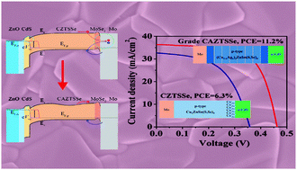
Although the substitution of Cu by Ag to suppress CuZn defects offers several advantages in overcoming the large open-circuit voltage (Voc) deficit for Cu2ZnSn(S,Se)4 (CZTSSe) solar cells, an excellent performance has not been achieved to date primarily due to the Fermi level pinning at the CdS/absorber interface and large recombination at the absorber/Mo interface. Herein, we developed a composition grading strategy to achieve a V-shaped Ag-graded structure with a higher Ag content on both the back and front surfaces of the (Cu,Ag)2ZnSn(S,Se)4 (CAZTSSe) layer. The key advantages of this Ag-graded structure are as follows: the higher content towards the CdS/absorber interface can create weak n-type donor defects and retard Fermi level pinning, whereas the lower content at the interlayer maintains the conductivity and light absorption; moreover, the other higher content towards Mo back contact can effectively suppress the recombination and improve the utilization of long-wave incident light. By appropriately adjusting the Ag gradient, we demonstrated a significant increase in Voc, and an unexpected conversion efficiency of 11.2% was achieved. This is the highest efficiency achieved to date for Ag-substituted CZTSSe solar cells, and the result supports a new aspect that synthesis of a composition-graded CAZTSSe absorber has great potential for future research.


 Please wait while we load your content...