
High-efficiency humidity-stable planar perovskite solar cells based on atomic layer architecture†
Dibyashree
Koushik
*a,
Wiljan J. H.
Verhees
b,
Yinghuan
Kuang
a,
Sjoerd
Veenstra
b,
Dong
Zhang
b,
Marcel A.
Verheijen
ac,
Mariadriana
Creatore
ab and
Ruud E. I.
Schropp
 ab
ab
aPlasma and Materials Processing, Department of Applied Physics, Eindhoven University of Technology (TU/e), 5600 MB Eindhoven, The Netherlands. E-mail: d.koushik@tue.nl
bECN-Solliance, High Tech Campus 21, 5656 AE Eindhoven, The Netherlands
cPhilips Innovation Labs, High Tech Campus 11, 5656 AE Eindhoven, The Netherlands
First published on 21st November 2016
Abstract
Perovskite materials are drawing tremendous interest for photovoltaic solar cell applications, but are hampered by intrinsic material and device instability issues. Such issues can arise from environmental influences as well as from the chemical incompatibility of the perovskite layer with charge transport layers and electrodes used in the device stack. Several attempts have been made to address the instability issue, mostly concentrating on the substitution of the organic cations in the perovskite lattice, and on alternatives for the organic charge extraction layers, without laying much emphasis on stabilising the existing, conventional high efficiency methylammonium lead iodide/spiro-OMeTAD based devices. To address the latter issue, we utilized atomic layer deposition (ALD) as a straightforward and soft deposition process to conformally deposit Al2O3 on top of the perovskite absorber. An ultra-thin ALD Al2O3 film effectively protects the perovskite layer while it is sufficiently thin enough to provide a tunnel contact. The fabricated perovskite solar cells (PSCs) exhibit superior device performance with a stabilised power conversion efficiency (PCE) of 18%, a significant reduction in hysteresis loss, and enhanced long-term stability (beyond 60 days) as a function of the unencapsulated storage time in ambient air, under humidity conditions ranging from 40 to 70% at room temperature. PCE measurements after 70 days of humidity exposure show that the devices incorporating 10 cycles of ALD Al2O3 could significantly retard the humidity-induced degradation thereby retaining about 60–70% of its initial PCE, while that of the reference devices drops to a remaining 12% of their initial PCE. This work successfully addresses and tackles the problem of the hybrid organic–inorganic IV-halide perovskite solar cell’s instability in a humid environment, and the key findings pave the way to the upscaling of these devices.
Broader contextThe record laboratory efficiency of single junction crystalline silicon (c-Si) solar cells, the technology that rules the global photovoltaic market to date, is reaching its practical limits and is fundamentally hard to advance. In order to break the efficiency barriers for 1 sun solar modules, a perovskite/c-Si tandem cell approach is gathering wide attention. This approach can bring about a step change in performance over common c-Si based technology while keeping fabrication and installation costs close to present levels. Single junction perovskite solar cells have already witnessed a tremendous increase in the power conversion efficiency to over 22% proving themselves at par with the c-Si technology, but only in terms of the (initial) efficiency. The technology is hampered by other issues such as the material instability, hysteresis loss, small area devices, and poor device reliability which is making its successful commercialization challenging. We present a step forward towards durable applications of the perovskite solar cells highlighting an atomic-layer interface architectural approach to reduce the hysteresis loss in the perovskite solar cells and to strongly reduce its humidity induced device degradation. These assets are invaluable for perovskite solar cells, irrespective of whether they are used in single junction technologies or as top cells in hybrid technologies. |
Introduction
Solar cells based on organic–inorganic hybrid perovskites have recently achieved an astounding power conversion efficiency (PCE) of 22.1%1 placing themselves at the forefront of many of the current global photovoltaic (PV) technologies. Due to their tunable, wide bandgap range, Eg = 1.55–2.3 eV,2 low-cost simple fabrication processes,3–6 high charge carrier mobility,7 in combination with the short predicted energy payback time (in the order of months),8 the perovskite solar cell (PSC) technology emerges as a serious contender for application amongst the other existing 20%+ technologies. However, in order to scaleup the perovskite PV technology, the issue regarding the device lifetime needs to be addressed, which is a hurdle towards its successful commercialisation.Lewis bases such as water (H2O) have been identified as one of the key sources for the irreversible degradation of perovskite films and the related devices.9–11 The most conventional and widely used perovskite, the methylammonium lead iodide (CH3NH3PbI3) is highly unstable in oxygen and moisture due to the presence of the weak Pb–I ionic bonds and the volatile CH3NH3I component in its lattice structure. Previous work by Frost et al. has shown that a single H2O molecule is capable of triggering the decomposition of a stoichiometric unit of CH3NH3PbI3 into CH3NH3I and PbI2.12 Furthermore, this PbI2 product which is sparingly soluble in water13 presents a toxicological issue which can again hamper the outdoor applications of PSCs.
In order to circumvent this humidity-induced degradation, several efforts have been made to fabricate stable PSCs. The pioneering work of Kim et al. on solid-state mesoscopic heterojunction PSCs has shown the stability of unencapsulated devices stored for over 500 h in air at room temperature.14 The focus has been recently shifted primarily towards tuning the perovskite composition in view of obtaining a more stable active layer.2,15–18 The triple cation based PSCs fabricated by Saliba et al.18 have demonstrated stability for 250 h under a nitrogen atmosphere, but the stability in the presence of humidity still remains unknown. Other studies have demonstrated the use of hydrophobic hole-transport layers (HTLs)19–21 and a thick carbon based electrode in a HTL-free PSC,22 both of which could significantly prevent the moisture ingress, but subsequently sacrifice the overall PCE of the devices. Several investigations exist that have adopted an interface modification method for enhancing the stability of the PSCs, but mainly focus on retarding the formation of trap states in the TiO2 layer upon irradiation23,24 and on preventing the metal-atom migration into the underlying layers upon aging,25–27 without addressing the humidity instability issue.
In this work, we present an interface engineering approach using an ultra-thin atomic layer deposited (ALD) Al2O3 layer, deposited directly on the CH3NH3PbI3−δClδ (x = δ) perovskite films. This layer substantially seals off the underlying sensitive perovskite to humidity conditions and also provides protection from the other cell components during their respective depositions on top, and against moisture exposure,28 thus preventing premature device failure, and enabling enhanced stability against humidity. In addition, it does not preclude the formation of a low-resistance contact to the perovskite layer. Having Eg ∼ 6.4 eV,29 Al2O3 could be efficiently utilised in the layer stack of a solar cell only when applied as an extremely thin layer. ALD is hence well-suited to apply such a thin layer as the thickness can be precisely controlled at the Angstrom level by simply varying the number of ALD cycles.
Although “state-of-the-art” PSCs with 22% PCE have been recently demonstrated, for the present study we have chosen cells based on CH3NH3PbI3−δClδ perovskite with a more modest and reproducible PCE of 15% that could be achieved without any complex processing conditions,30 and do not opt for the mixed cation mixed anion PSC approach. However, with the incorporation and optimization of the ALD Al2O3 into the device stack, the PCE of these cells significantly increases to a stabilized 18%. The hysteresis in the cells is clearly reduced and the stability of the cells against humidity is unprecedentedly enhanced.
Results and discussion
First, the presence of the ultra-thin ALD Al2O3 is investigated on top of the individual thin films of perovskite on glass using X-ray photoelectron spectroscopy (XPS). Fig. 1a presents the Al 2p peak centred at a binding energy of 74.6 eV, confirming the composition of Al2O3 obtained for 10 ALD cycles. The O 1s peak shown in Fig. 1b is centered at a binding energy of 531.5 eV pertaining to the characteristic formation of Al–O bonds on the perovskite film.11,31 The peak with the binding energy at 402.7 eV is ascribed to the N element in the perovskite, indicating no consumption of CH3NH3+ during the ALD process. Furthermore, the absence of the peak at 139.1 eV (binding energy of Pb–I) confirms that there is no formation of the PbI2 degradation product32 in the pristine perovskite film attributing the stability of the same towards the utilized ALD deposition conditions. Meanwhile, there is no observance of the Cl 2p peak which confirms that even though PbCl2 is used as one of the initial precursors for the formation of the CH3NH3PbI3−δClδ perovskite, most of it is dissociated into Pb2+ and 2Cl− and the chlorine is substantially removed during the perovskite film formation (XPS spectra of Pb, I, N, C and Cl are shown in Fig. S1 in the ESI†). Fig. 1c shows the X-ray diffraction (XRD) spectra of the perovskite films before and after the successive depositions of 10 and 20 cycles of ALD Al2O3 on top. There is no change in the crystalline structure of the perovskite film before and after the deposition, as confirmed by the perovskite characteristic peaks at 14.1°, 28.4°, 30.9°, 35.1° and 43.2°, that can be assigned to the (110), (220), (213), (312) and (330) reflections of CH3NH3PbI3, respectively,9,33 and the absence of signatures of other phases. Previous work by Dong et al. used trimethylaluminium (TMA) and ozone (O3) to apply an ALD Al2O3 capping layer on top of the perovskite at a temperature of 70 °C due to the high sensitivity of the perovskites to H2O and temperature. But, even with this dedicated recipe, just 1 cycle of ALD Al2O3 on top was sufficient to degrade the perovskite which was confirmed by the appearance of a small intensity PbI2 peak at 12.6° in the XRD spectra.9 In contrast, our ALD Al2O3 process, using TMA and H2O vapor as the aluminium and oxygen precursors respectively, at 100 °C with a similar growth per cycle (GPC) of about 0.1 nm, appears to be far less detrimental to the underlying perovskite layer. It is speculated that the use of H2O, which is less oxidizing than O3, makes it possible to deposit ALD Al2O3 directly on these sensitive perovskite layers, even at a comparatively higher temperature.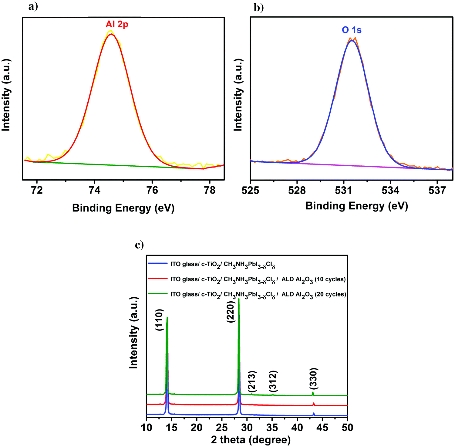 | ||
| Fig. 1 Surface XPS spectra of (a) Al 2p and (b) O 1s peak of a 10 cycle ALD Al2O3 layer on top of the perovskite film. (c) XRD spectra of the parent perovskite film before and after the successive depositions of ALD Al2O3. | ||
Having proven the crystallographic stability of the perovskite films upon application of the chosen ALD Al2O3 process, the effect of Al2O3 layer thickness is addressed by fabricating a series of complete solar cells with an increasing number of cycles of ALD Al2O3 (varied between 2 and 20 cycles) introduced at the perovskite/HTL interface. Fig. 2a shows a bright field transmission electron microscopy (TEM) image of the cross-section of a complete planar perovskite solar cell. A 150 nm thick tin doped indium oxide (ITO)/glass layer has been used as the front electrode (cathode). As the electron transport layer (ETL), a 50 nm thick compact titanium dioxide (c-TiO2) is deposited on top of the ITO. CH3NH3PbI3−δClδ with a thickness of 300 nm is used as the photoactive layer. An ultra-thin ALD Al2O3 layer (20 ALD cycles, corresponding to ∼2 nm) covers the top of the perovskite layer. 180 nm 2,2′,7,7′-tetrakis(N,N-di-p-methoxyphenyl-amine)9,9′-spirobifluorene (Spiro-OMeTAD) and 100 nm Au serve as the HTL and the back electrode (anode), respectively. The detailed fabrication procedure of the perovskite and other associated layers in the device stack can be found in the Methods section. The cross-section TEM image in Fig. 2a does not present an explicit view of this ultra-thin ALD layer since the perovskite–HTL interface is inclined to the cross-section of the TEM sample hindering its distinct visibility. A top-view scanning electron microscopy (SEM) image of the perovskite film is shown in the ESI† as Fig. S2. As represented, the synthesized perovskite films are characterized by large micrometer sized grains rendering an expected reduced bulk defect density in the film together with suppressed charge trapping during device operation.34
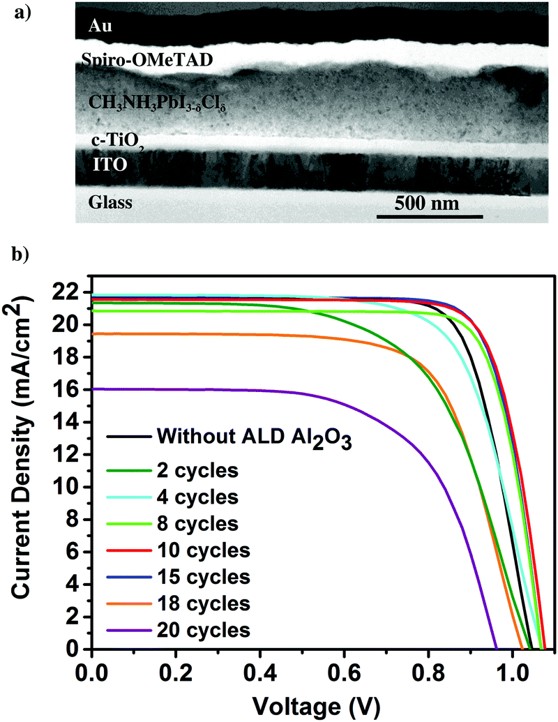 | ||
| Fig. 2 (a) Bright field TEM cross-sectional image of the complete planar perovskite device incorporating the ALD Al2O3 at the perovskite/HTL interface. (b) J–V curves of the best perovskite devices utilizing different numbers of ALD Al2O3 cycles. | ||
The photocurrent density–voltage (J–V) characteristics of these cells are shown in Fig. 2b. A typical device without an Al2O3 layer produces a short-circuit current density Jsc of 21.3 mA cm−2, an open-circuit voltage Voc of 1.03 V and a fill factor FF of 0.69 yielding a PCE of 15.1%. In equivalent devices incorporating the thin ALD Al2O3 layer, considerable improvement in all the PV parameters, especially FF, is observed. This is attributed to the suppressed recombination at or near the HTL due to the incorporation of the ALD Al2O3 layer on top of the perovskite. Thus, the Al2O3 layer could be acting as a passivation layer on top of the perovskite surface, as was also shown by Adhyaksa et al. using carrier diffusion length measurements in single layers.35 In addition, previously reported results using porous Al2O3 nanoparticles at the perovskite/Spiro-OMeTAD interface,27 Al3+ ions doping in the perovskite layer,36 and pulsing ALD TMA vapor on perovskite nanocrystals,37 could also be related to this passivation effect. The best ALD-treated perovskite device is achieved with 10 cycles of Al2O3 resulting in a Jsc of 21.7 mA cm−2, Voc of 1.08 V, FF of 0.77 and PCE of 18%, enabling a 3% efficiency enhancement with respect to the reference device. The high FF indicates that a low resistive contact, or a tunnelling contact, is maintained between the perovskite and the Spiro-OMeTAD HTL. However, the range between 10 and 15 cycles of ALD Al2O3 seems to be the optimum range in terms of efficient perovskite PV devices. For 2–8 cycles of ALD Al2O3, the J–V results are sub optimal. This is thought to be due to incomplete coverage of the ALD layer so that the initial exposure to H2O vapor still has a dominant deleterious effect. Increasing the number of cycles beyond 15, on the other hand, also significantly deteriorates the Jsc and the FF. This can be attributed to the thickness of the ALD Al2O3 beyond a suitable tunnelling thickness, and concomitantly, the reduction of hole injection and transport from the perovskite layer to the HTL due to an increasing number of ALD cycles leading to the formation of a relatively thick ALD Al2O3 insulating layer. The J–V parameters of the pristine and all the ALD Al2O3 incorporating perovskite devices are summarised in Table 1. The statistical box plots of the PV parameters (Jsc, Voc, FF, and PCE) of the devices incorporating different numbers of ALD Al2O3 cycles can be found in Fig. S3 (ESI†).
| Configuration | V oc (V) | J sc (mA cm−2) | FF | PCE (%) |
|---|---|---|---|---|
| Pristine | 1.03 | 21.3 | 0.69 | 15.1 |
| Al2O3, 2 cycles | 1.04 | 21.3 | 0.61 | 13.5 |
| Al2O3, 4 cycles | 1.06 | 21.9 | 0.69 | 16.0 |
| Al2O3, 8 cycles | 1.07 | 20.8 | 0.78 | 17.4 |
| Al2O3, 10 cycles | 1.08 | 21.7 | 0.77 | 18.0 |
| Al2O3, 15 cycles | 1.07 | 21.7 | 0.77 | 17.9 |
| Al2O3, 18 cycles | 1.02 | 19.5 | 0.69 | 13.7 |
| Al2O3, 20 cycles | 0.96 | 16.0 | 0.63 | 9.7 |
In order to further study the presence and conformality of this ultra-thin ALD Al2O3 layer at the perovskite/HTL interface, energy dispersive X-ray (EDX) elemental mappings are acquired on several perovskite/HTL interface regions. A more detailed High Angle Annular Dark Field (HAADF) scanning TEM image of the perovskite/HTL interface is shown in Fig. 3a. An ultra-thin interfacial layer is distinctly visible which marks the presence of ALD Al2O3. This is in accordance with the corresponding elemental maps of Al and O in Fig. 3c and d respectively. The other associated elements C, N, Pb and I present in the perovskite and the HTL are shown in Fig. 3e–h. The overlapping elemental mapping image shown in Fig. 3b demonstrates the ALD Al2O3 layer covering the perovskite surface. Note that the elemental mapping analysis was carried out at three different perovskite/HTL cross-sectional locations and similar distribution maps were obtained as shown in Fig. S4 and S6 (ESI†). The EDX line scan profile in Fig. 3i depicts the two strong intensity peaks of Al and O present at the perovskite/HTL interface. This is clear and unambiguous evidence of the presence of this ultra-thin layer in the actual solar cell device stack.
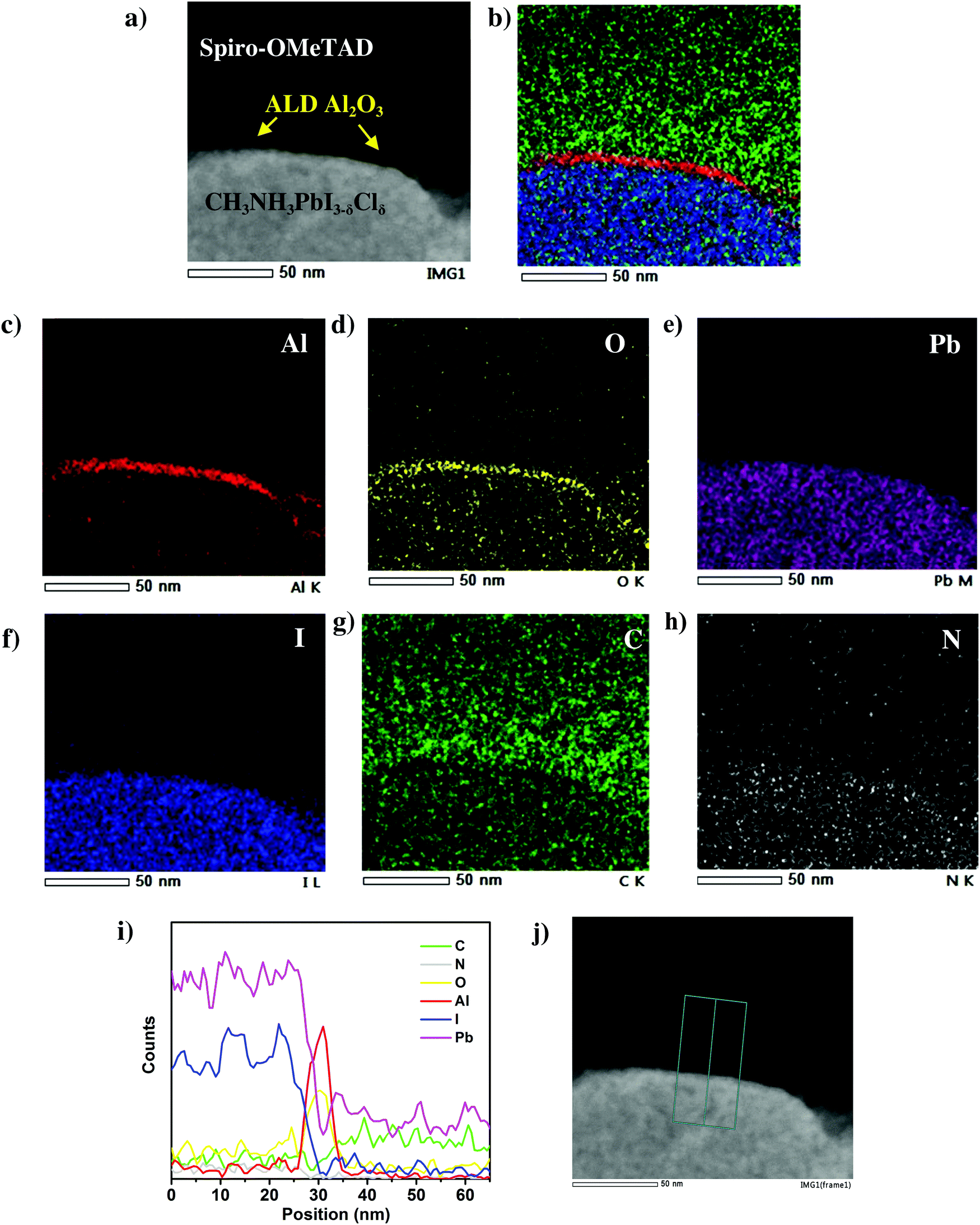 | ||
| Fig. 3 (a) High angle annular dark field (HAADF) scanning TEM image of the enlarged perovskite/ALD Al2O3/Spiro-OMeTAD interface. (b) Corresponding overlapping elemental mapping image. (c–h) Individual elemental maps of Al, O, Pb, I, C and N. (i) Compositional profiles at the perovskite/ALD Al2O3/Spiro-OMeTAD interface, constructed from a 2-dimensional EDX map by averaging over the area indicated by the cyan box in the corresponding perovskite/HTL interface (j). | ||
The perovskite device architecture plays an important role in its hysteretic response,38–41 which is one of the vital issues curbing the development of the PSCs in spite of its rapidly increasing high efficiencies. PSCs based on a mesoporous structure and organic charge extraction layers tend to exhibit lower hysteresis as compared to cells based on a planar configuration where the perovskite is crystallized on top of a compact ETL layer, and is considered to originate at the perovskite/metal oxide interface (in our case TiO2). To further explicate the effect of our ultra-thin ALD Al2O3 towards the J–V hysteresis, both the reference and Al2O3 incorporated devices were measured at a scan rate of 10 mV s−1 in forward and backward directions under simulated AM 1.5 radiation of 1000 W m−2. It is worth mentioning that with regards to the J–V measurements, 10 cycles of ALD Al2O3 are considered to be the optimum in our case (Table 1), and hence, this Al2O3 coverage is utilized in our further studies (unless mentioned otherwise). As shown in Fig. 4a, the cells based on ALD Al2O3 are seen to experience a significant reduction in J–V hysteresis as compared to the ones without. This can be ascribed to the reduction of electronic defects at the perovskite surface when the ultra-thin ALD Al2O3 layer is deposited on top. This reduction aids in suppressing the trap–assisted recombination which is speculated to be one of the causes of the origin of the hysteresis behavior in the PSCs,40,42 other than ion migration40,43,44 and ferroelectricity.40,44 A similar reduction of hysteresis has been recently reported by Wang et al. while doping the perovskite with Al3+ ions.36Fig. 4b shows the stabilized maximum power point (MPP) tracking results of the best perovskite devices with and without the ALD Al2O3 interfacial layer. A steady-state PCE of 18% is measured for the Al2O3 incorporated cells and a PCE of 15% for the reference cells, both of which are in agreement with the efficiencies obtained from the respective J–V curves. The external quantum efficiency (EQE) of both these cell types is shown in Fig. 4c. The enhanced blue response in the EQE spectra of the ALD Al2O3 layer incorporating device seems to be correlated with an optical absorbance improvement that we also see for short wavelengths in individual perovskite absorber layers with Al2O3 coating after 70 days of humidity exposure (see Fig. S10, ESI†). It is not clear what causes the enhanced absorptance, but changes in optical properties have been found earlier in PSCs accommodating different cell designs,31,45 and also upon ageing.46 The Jsc calculated from the integration of the EQE over the AM 1.5 solar spectrum at 1000 W m−2 is also represented in Fig. 4c, and is measured to be 20.3 mA cm−2 for the reference device and 20.7 mA cm−2 for the ALD based device. There is ∼1 mA cm−2 error between the Jsc obtained from the J–V measurements and that from the EQE measurements under simulated sunlight. This is quite common for thin film solar cells on glass and has been attributed to the difference in small spot measurements in EQE and complete flooding of the cell in light in the J–V measurements.47 The J–V parameters of the forward and backward scans are presented in Table 2.
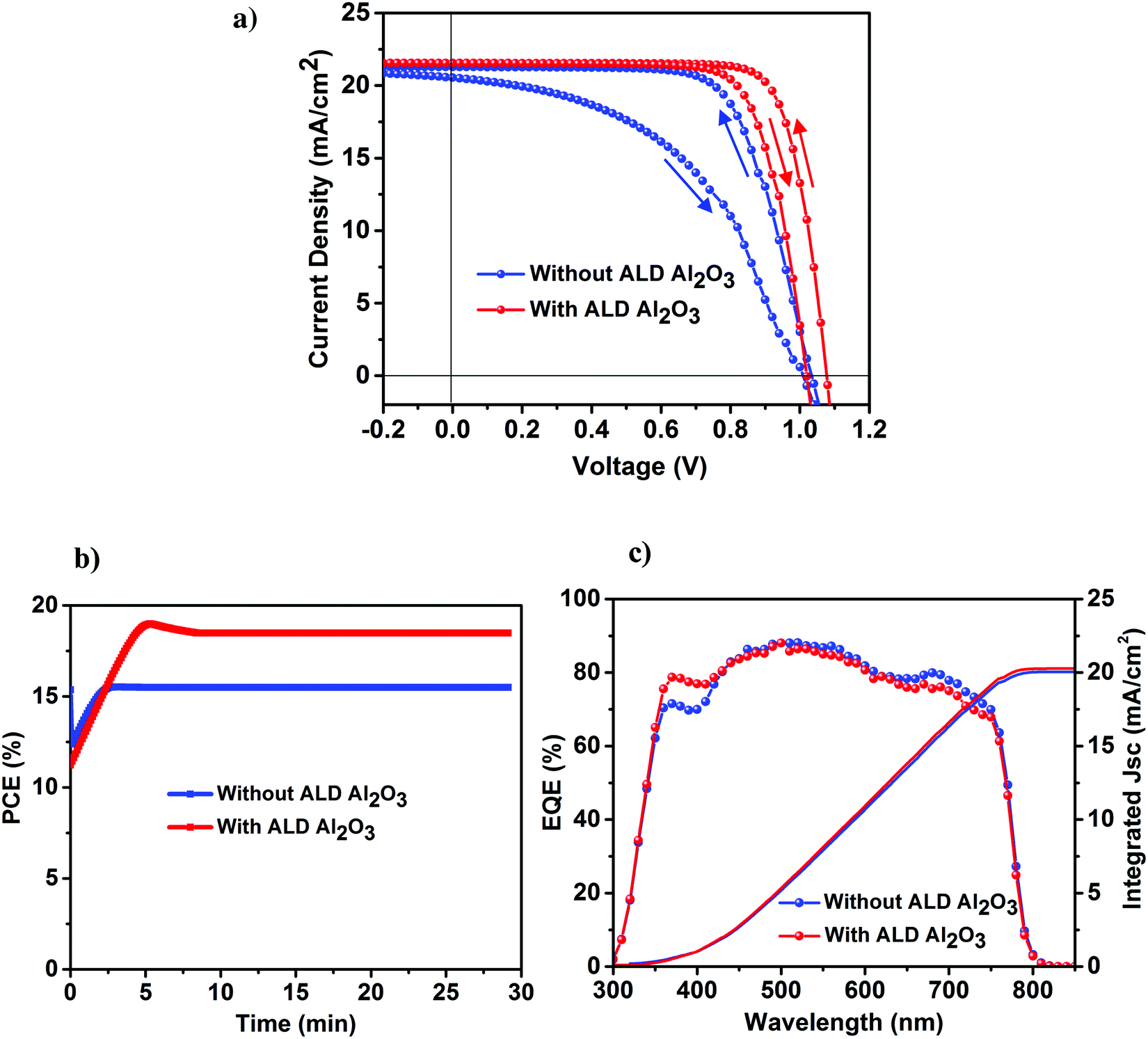 | ||
| Fig. 4 (a) Forward and backward scanned J–V curves of the champion perovskite devices with and without the ALD Al2O3 (10 cycles) interfacial layer. The J–V curves are measured at a scan rate of 10 mV s−1 in forward (−0.2 to 1.2 V) and backward (1.2 to −0.2 V) directions under simulated AM 1.5 radiation of 1000 W m−2. (b) MPP tracking for 30 min to obtain the steady-state PCE. (c) Comparative EQE spectra of both the devices along with their respective integrated Jsc curves. | ||
| Configuration | Scan direction | V oc (V) | J sc (mA cm−2) | FF | PCE (%) |
|---|---|---|---|---|---|
| Without ALD Al2O3 | Forward | 1.0 | 20.8 | 0.48 | 9.9 |
| Backward | 1.03 | 21.3 | 0.69 | 15.1 | |
| With ALD Al2O3 (10 cycles) | Forward | 1.02 | 21.4 | 0.76 | 16.6 |
| Backward | 1.08 | 21.7 | 0.77 | 18.0 |
In view of the role of the perovskite contacting ALD Al2O3 layer as a protection layer against humidity,48 an aging study of the perovskite films and the devices are performed under various humidity conditions. First, the structural integrity and photovoltaic performance of the PSCs (with and without the ALD layer) is monitored under a N2 atmosphere for several weeks prior to exposure to humidity. This is conducted to discern between the effect of humidity and the instabilities related to the utilized organic HTL, towards the degradation of the PSCs. Then, the devices are exposed to 40% humidity conditions (for 15 days), then to 60% humidity (10 more days) and finally, to ambient laboratory humidity conditions which are between 50 and 70% (the average ambient humidity range in the Netherlands during the study period) for 30 more days. XRD measurements are performed over time to monitor the comparative structural stability of the films. The parent perovskite film starts to degrade after being exposed to 60% humidity for 10 days as is evident from the appearance of a new signature peak at 12.6° in the XRD spectra9,11 as shown in Fig. 5a. This peak is assigned to the (001) diffraction peak of PbI2 which is formed as a result of the decomposition of CH3NH3PbI3 when exposed to oxygen and moisture. In contrast, this peak is not detected in the case of the Al2O3/perovskite samples as shown in Fig. 5b, thus pointing out the role of Al2O3 towards circumventing humidity induced perovskite degradation.
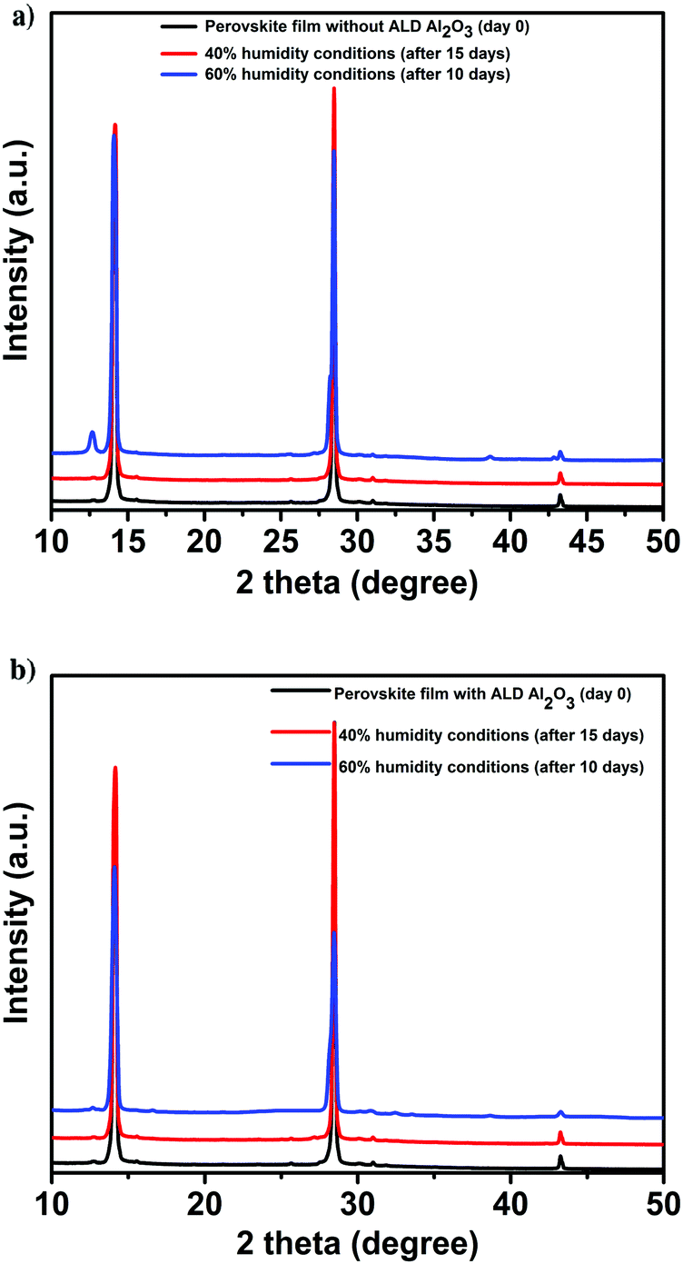 | ||
| Fig. 5 XRD of the perovskite films before and after exposure to varied humidity conditions. (a) Pristine. (b) With ALD Al2O3. | ||
The PV parameters of the unencapsulated PSCs acquired during the course of the humidity aging study are depicted in Fig. 6. The J–V measurements of these cells have been performed at room temperature in ambient air every alternate day, and the devices have been kept in the dark between successive measurements. Comparing the performance of the PSCs with and without the ALD Al2O3, it is evident that the PCE of the reference device starts to decrease just after 15 days although kept under a N2 atmosphere, while the Al2O3 incorporated ones are not much affected. Carrying forward our study for a course of 70 days with a stepwise increase in humidity conditions (from 40% to 50–70%), it is observed that the ALD Al2O3 significantly delays the humidity-induced degradation, thereby retaining about 70% of the initial PCE, while the pristine devices reach nearly a dead point with only 12% of its initial PCE remaining. The same conclusion can be drawn from the MPP tracking which is performed on the best devices of both the configurations after 70 days of aging (Fig. 7a). The PV parameters at the start and at the end of the aging study are summarised in Table 3. Also, the J–V curves of the parent and ALD Al2O3 incorporated cells (both 4 and 10 cycles) are shown in Fig. S7, S8 and S9 (ESI†) respectively. The histogram of the PCE statistics of 25 ALD Al2O3/PSCs is shown in Fig. 7b. It is worth mentioning that, as perceptible from Fig. 6d, oxygen and moisture apparently deteriorate both configurations with and without Al2O3, but the ALD Al2O3 devices show distinctly stable behaviour of Jsc and Voc, attributed to significantly better shielding against the penetration of the moisture into the sensitive perovskite layer under the applied humidity conditions. The ALD Al2O3 layer directly on the perovskite chemically passivates the surface defects present on the perovskite, therefore inducing more stability towards H2O and O2 induced defects. Furthermore, its hydrophobicity49 may impede the permeation of H2O.
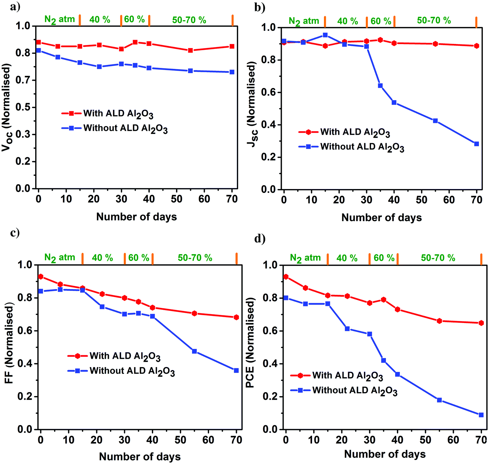 | ||
| Fig. 6 Normalized PV parameters (a) Voc, (b) Jsc, (c) FF, and (d) PCE of the champion perovskite devices with and without ALD Al2O3 as a function of storage time under varied humidity conditions. | ||
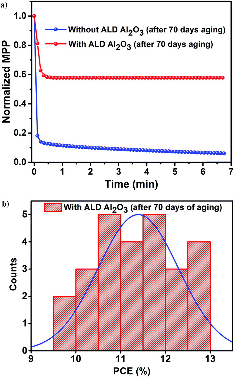 | ||
| Fig. 7 (a) MPP tracking of the best devices. (b) Histogram of the PCE of 25 perovskite/ALD Al2O3 devices after 70 days of a humidity aging study. | ||
| Configuration | V oc (V) | J sc (mA cm−2) | FF | PCE (%) | |
|---|---|---|---|---|---|
| Without ALD Al2O3 | Fresh | 1.03 | 21.3 | 0.69 | 15.1 |
| After 70 days | 0.86 | 6.8 | 0.31 | 1.8 | |
| With ALD Al2O3 (10 cycles) | Fresh | 1.08 | 21.7 | 0.77 | 18.0 |
| After 70 days | 1.05 | 21.3 | 0.56 | 13.0 |
We propose the extension of the implementation of the ALD Al2O3 layer into the less hydrophilic cation (formamidium, cesium) based, bromide or mixed halide based or the mixed cation mixed anion based PSCs, where the active perovskite layer is comparatively more stable than the perovskite used in our work, where it could remarkably contribute and add to the extended device stability which otherwise is solely derived from the intrinsic stability of the absorber and the utilized charge extraction layers. Also, it is expected that apart from protecting against humidity during the lifetime of the solar cell, this layer may be effective in protecting the perovskite layer during successive depositions of a wider range of electron selective or hole selective contact layers.
Conclusions
An ultra-thin ALD Al2O3 layer is inserted into the conventional thin film n–i–p architecture of CH3NH3PbI3−δClδ PSCs in order to reduce the hysteresis loss and at the same time stabilize the devices against humid conditions. An absolute 3% increase in the PCE is observed in the best perovskite/ALD Al2O3 device exhibiting a PCE of 18% along with a significant reduction in the hysteresis loss. The unencapsulated Al2O3 incorporating devices exhibit a remarkable stability against ambient humidity retaining 60–70% of the initial PCE after 70 days, while the reference cells without the Al2O3 layer experience a drastic fall to 12% of its initial PCE during the study period. Our work is a manifestation towards preventing humidity induced degradation via interface engineering in PSCs with ALD Al2O3, and could be implemented in other contemporary PSC embodiments including the state-of-the-art devices with 22% PCE. It could bring us one step ahead in realizing the commercialisation of high efficiency and humidity stable PSCs.Methods
Materials
Pb(CHCO2)2·3H2O (PbAc2, Aldrich, 99.999%), PbCl2 (Alpha Aesar 99.999%), CH3NH3I (MAI, Dyesol), Spiro-OMeTAD (Lumtec), lithium bis(trifluoromethanesulfonyl) imide (LitFSI, Aldrich 99.95%), and 4-tert-butylpyridine (tBP, Aldrich 96%).Solar cell fabrication
ITO coated glass substrates (Naranjo substrates) are ultrasonically cleaned for 10 minutes in detergent (Extran MA01), deionized water and iso-propanol. The dense TiO2 layer is deposited by e-beam deposition (O2 flow of 12 sccm, pressure of 4.7 × 10⁻⁴ mbar, deposition rate of 0.05 nm s−1).50 The perovskite precursor solution is made by mixing PbAc2, PbCl2 and MAI in dimethylformamide (DMF) as reported elsewhere.30 The precursor solution is spincoated on top of the TiO2 layer in a N2 filled glovebox at 3000 rpm for 60 s. The perovskite layer is formed by annealing at 130 °C for 10 min. ALD Al2O3 is deposited on top of the perovskite/TiO2/ITO glass in an Oxford Instrument OpAL™ reactor. Each ALD cycle consists of a trimethylaluminium (Al(CH3)3) dose of 0.02 s, followed by a purge of 3.5 s, then a H2O vapor dose of 0.1 s, followed by a purge of 3.5 s. The thickness of the ALD Al2O3 layers is characterized using in situ spectroscopic ellipsometry. SpiroOMeTAD solution is spincoated at 2000 rpm (80 mg ml−1 in chlorobenzene doped with 28.5 μl tBP and 17.5 μl of a 520 mg ml−1 solution of LitFSI in acetonitrile). The devices are exposed to air overnight for O2 doping of the SpiroOMeTAD and then finally finished with 100 nm thick gold contacts deposited on top via thermal evaporation.Acknowledgements
The authors thank Henriette Gatz (TU/e), Leon W. Veldhuizen (TU/e), and Dr Valerio Zardetto (TU/e) for the valuable discussions; Jeroen van Gerwen (TU/e), Christian A. A. van Helvoirt (TU/e), Klaas J. Bakker (ECN), and Maarten Dörenkämper (ECN) for the technical support. The authors are grateful to Dr Beatriz Barcones (TU/e) for the TEM sample preparation and Akhil Sharma (TU/e) for the assistance with the SEM imaging. Solliance is acknowledged for funding the TEM facility. This work is supported by the Light Management in New Photovoltaic Materials (LMPV) research program of the Foundation for Fundamental Research on Matter (FOM), which is part of the Netherlands Organization for Scientific Research (NWO).References
- NREL. Best Research-Cell Efficiencies http://www.nrel.gov/ncpv/images/efficiency_chart.jpg (accessed September 1, 2016).
- J. H. Noh, S. H. Im, J. H. Heo, T. N. Mandal and S. I. Seok, Nano Lett., 2013, 13, 1764–1769 CrossRef CAS PubMed.
- M. M. Lee, J. Teuscher, T. Miyasaka, T. N. Murakami and H. J. Snaith, Science, 2012, 338, 643 CrossRef CAS PubMed.
- N. J. Jeon, J. H. Noh, W. S. Yang, Y. C. Kim, S. Ryu, J. Seo and S. I. Seok, Nature, 2015, 517, 476–480 CrossRef CAS PubMed.
- J. Burschka, N. Pellet, S.-J. Moon, R. Humphry-Baker, P. Gao, M. K. Nazeeruddin and M. Gratzel, Nature, 2013, 499, 316–319 CrossRef CAS PubMed.
- O. Malinkiewicz, A. Yella, Y. H. Lee, G. M. Espallargas, M. Graetzel, M. K. Nazeeruddin and H. J. Bolink, Nat. Photonics, 2014, 8, 128–132 CrossRef CAS.
- G. Xing, N. Mathews, S. Sun, S. S. Lim, Y. M. Lam, M. Grätzel, S. Mhaisalkar and T. C. Sum, Science, 2013, 342, 344 CrossRef CAS PubMed.
- J. Gong, S. B. Darling and F. You, Energy Environ. Sci., 2015, 8, 1953–1968 CAS.
- X. Dong, X. Fang, M. Lv, B. Lin, S. Zhang, J. Ding and N. Yuan, J. Mater. Chem. A, 2015, 3, 5360–5367 CAS.
- D. Li, S. A. Bretschneider, V. W. Bergmann, I. M. Hermes, J. Mars, A. Klasen, H. Lu, W. Tremel, M. Mezger, H.-J. Butt, S. A. L. Weber and R. Berger, J. Phys. Chem. C, 2016, 120, 6363–6368 CAS.
- G. Niu, W. Li, F. Meng, L. Wang, H. Dong and Y. Qiu, J. Mater. Chem. A, 2014, 2, 705–710 CAS.
- J. M. Frost, K. T. Butler, F. Brivio, C. H. Hendon, M. van Schilfgaarde and A. Walsh, Nano Lett., 2014, 14, 2584–2590 CrossRef CAS PubMed.
- H. L. Clever and F. J. Johnston, J. Phys. Chem. Ref. Data, 1980, 9, 751–784 CrossRef CAS.
- H.-S. Kim, C.-R. Lee, J.-H. Im, K.-B. Lee, T. Moehl, A. Marchioro, S.-J. Moon, R. Humphry-Baker, J.-H. Yum, J. E. Moser, M. Grätzel and N.-G. Park, Sci. Rep., 2012, 2, 591 Search PubMed.
- X. Li, M. Ibrahim Dar, C. Yi, J. Luo, M. Tschumi, S. M. Zakeeruddin, M. K. Nazeeruddin, H. Han and M. Grätzel, Nat. Chem., 2015, 7, 703–711 CrossRef CAS PubMed.
- I. C. Smith, E. T. Hoke, D. Solis-Ibarra, M. D. McGehee and H. I. Karunadasa, Angew. Chem., 2014, 126, 11414–11417 CrossRef.
- J.-W. Lee, D.-H. Kim, H.-S. Kim, S.-W. Seo, S. M. Cho and N.-G. Park, Adv. Energy Mater., 2015, 5, 1501310 CrossRef.
- M. Saliba, T. Matsui, J.-Y. Seo, K. Domanski, J.-P. Correa-Baena, M. K. Nazeeruddin, S. M. Zakeeruddin, W. Tress, A. Abate, A. Hagfeldt and M. Gratzel, Energy Environ. Sci., 2016, 9, 1989–1997 CAS.
- L. Zheng, Y.-H. Chung, Y. Ma, L. Zhang, L. Xiao, Z. Chen, S. Wang, B. Qu and Q. Gong, Chem. Commun., 2014, 50, 11196–11199 RSC.
- T. Leijtens, T. Giovenzana, S. N. Habisreutinger, J. S. Tinkham, N. K. Noel, B. A. Kamino, G. Sadoughi, A. Sellinger and H. J. Snaith, ACS Appl. Mater. Interfaces, 2016, 8, 5981–5989 CAS.
- Y. S. Kwon, J. Lim, H.-J. Yun, Y.-H. Kim and T. Park, Energy Environ. Sci., 2014, 7, 1454–1460 CAS.
- A. Mei, X. Li, L. Liu, Z. Ku, T. Liu, Y. Rong, M. Xu, M. Hu, J. Chen, Y. Yang, M. Grätzel and H. Han, Science, 2014, 345, 295 CrossRef CAS PubMed.
- S. Ito, S. Tanaka, K. Manabe and H. Nishino, J. Phys. Chem. C, 2014, 118, 16995–17000 CAS.
- Y. H. Lee, J. Luo, M.-K. Son, P. Gao, K. T. Cho, J. Seo, S. M. Zakeeruddin, M. Grätzel and M. K. Nazeeruddin, Adv. Mater., 2016, 28, 3966–3972 CrossRef CAS PubMed.
- K. Domanski, J.-P. Correa-Baena, N. Mine, M. K. Nazeeruddin, A. Abate, M. Saliba, W. Tress, A. Hagfeldt and M. Grätzel, ACS Nano, 2016, 10, 6306–6314 CrossRef CAS PubMed.
- M. Kaltenbrunner, G. Adam, E. D. Glowacki, M. Drack, R. Schwodiauer, L. Leonat, D. H. Apaydin, H. Groiss, M. C. Scharber, M. S. White, N. S. Sariciftci and S. Bauer, Nat. Mater., 2015, 14, 1032–1039 CrossRef CAS PubMed.
- S. Guarnera, A. Abate, W. Zhang, J. M. Foster, G. Richardson, A. Petrozza and H. J. Snaith, J. Phys. Chem. Lett., 2015, 6, 432–437 CrossRef CAS PubMed.
- J. Yang, B. D. Siempelkamp, D. Liu and T. L. Kelly, ACS Nano, 2015, 9, 1955–1963 CrossRef CAS PubMed.
- G. Dingemans and W. M. M. Kessels, J. Vac. Sci. Technol., A, 2012, 30, 040802 Search PubMed.
- W. Qiu, T. Merckx, M. Jaysankar, C. Masse de la Huerta, L. Rakocevic, W. Zhang, U. W. Paetzold, R. Gehlhaar, L. Froyen, J. Poortmans, D. Cheyns, H. J. Snaith and P. Heremans, Energy Environ. Sci., 2016, 9, 484–489 CAS.
- H. Wei, J. Shi, X. Xu, J. Xiao, J. Luo, J. Dong, S. Lv, L. Zhu, H. Wu, D. Li, Y. Luo, Q. Meng and Q. Chen, Phys. Chem. Chem. Phys., 2015, 17, 4937–4944 RSC.
- W. Li, J. Li, G. Niu and L. Wang, J. Mater. Chem. A, 2016, 4, 11688–11695 CAS.
- X. Guo, C. McCleese, C. Kolodziej, A. C. S. Samia, Y. Zhao and C. Burda, Dalton Trans., 2016, 45, 3806–3813 RSC.
- W. Nie, H. Tsai, R. Asadpour, J.-C. Blancon, A. J. Neukirch, G. Gupta, J. J. Crochet, M. Chhowalla, S. Tretiak, M. A. Alam, H.-L. Wang and A. D. Mohite, Science, 2015, 347, 522–525 CrossRef CAS PubMed.
- G. W. P. Adhyaksa, L. W. Veldhuizen, Y. Kuang, S. Brittman, R. E. I. Schropp and E. C. Garnett, Chem. Mater., 2016, 28, 5259–5263 CrossRef CAS.
- J. T.-W. Wang, Z. Wang, S. Pathak, W. Zhang, D. W. deQuilettes, F. Wisnivesky-Rocca-Rivarola, J. Huang, P. K. Nayak, J. B. Patel, H. A. Mohd Yusof, Y. Vaynzof, R. Zhu, I. Ramirez, J. Zhang, C. Ducati, C. Grovenor, M. B. Johnston, D. S. Ginger, R. J. Nicholas and H. J. Snaith, Energy Environ. Sci., 2016, 9, 2892–2901 CAS.
- G. Li, F. W. R. Rivarola, N. J. L. K. Davis, S. Bai, T. C. Jellicoe, F. de la Peña, S. Hou, C. Ducati, F. Gao, R. H. Friend, N. C. Greenham and Z.-K. Tan, Adv. Mater., 2016, 28, 3528–3534 CrossRef CAS PubMed.
- E. L. Unger, E. T. Hoke, C. D. Bailie, W. H. Nguyen, A. R. Bowring, T. Heumuller, M. G. Christoforo and M. D. McGehee, Energy Environ. Sci., 2014, 7, 3690–3698 CAS.
- H.-S. Kim and N.-G. Park, J. Phys. Chem. Lett., 2014, 5, 2927–2934 CrossRef CAS PubMed.
- H. J. Snaith, A. Abate, J. M. Ball, G. E. Eperon, T. Leijtens, N. K. Noel, S. D. Stranks, J. T.-W. Wang, K. Wojciechowski and W. Zhang, J. Phys. Chem. Lett., 2014, 5, 1511–1515 CrossRef CAS PubMed.
- H.-W. Chen, N. Sakai, M. Ikegami and T. Miyasaka, J. Phys. Chem. Lett., 2015, 6, 164–169 CrossRef CAS PubMed.
- T. Heiser and E. R. Weber, Phys. Rev. B: Condens. Matter Mater. Phys., 1998, 58, 3893–3903 CrossRef CAS.
- K. Yamada, K. Isobe, E. Tsuyama, T. Okuda and Y. Furukawa, Solid State Ionics, 1995, 79, 152–157 CrossRef CAS.
- A. Dualeh, T. Moehl, N. Tétreault, J. Teuscher, P. Gao, M. K. Nazeeruddin and M. Grätzel, ACS Nano, 2014, 8, 362–373 CrossRef CAS PubMed.
- M. M. Lee, J. Teuscher, T. Miyasaka, T. N. Murakami and H. J. Snaith, Science, 2012, 338, 643–647 CrossRef CAS PubMed.
- A. Sadhanala, F. Deschler, T. H. Thomas, S. E. Dutton, K. C. Goedel, F. C. Hanusch, M. L. Lai, U. Steiner, T. Bein, P. Docampo, D. Cahen and R. H. Friend, J. Phys. Chem. Lett., 2014, 5, 2501–2505 CrossRef CAS PubMed.
- W. Reetz, T. Kirchartz, A. Lambertz, J. Hüpkes and A. Gerber, Proceedings of the 24th European Photovoltaic Solar Energy Conference, Hamburg, Germany, 2009, pp. 2784–2788 Search PubMed.
- E. Langereis, M. Creatore, S. B. S. Heil, M. C. M. van de Sanden and W. M. M. Kessels, Appl. Phys. Lett., 2006, 89, 081915 CrossRef.
- L.-C. Wang, Y.-Y. Han, K.-C. Yang, M.-J. Chen, H.-C. Lin, C.-K. Lin and Y.-T. Hsu, Surf. Coat. Technol., 2016, 305, 158–164 CrossRef CAS.
- W. Qiu, U. W. Paetzold, R. Gehlhaar, V. Smirnov, H.-G. Boyen, J. G. Tait, B. Conings, W. Zhang, C. B. Nielsen, I. McCulloch, L. Froyen, P. Heremans and D. Cheyns, J. Mater. Chem. A, 2015, 3, 22824–22829 CAS.
Footnote |
| † Electronic supplementary information (ESI) available: Characterization methods, box plot of the perovskite solar cells using different cycles of ALD Al2O3, XRD spectra of the perovskite devices during the aging study, additional TEM and elemental mapping images of the perovskite/ALD Al2O3 interface taken at different cross-sectional locations, J–V curves of the devices with and without ALD Al2O3 measured during the 70 days course of the aging study. See DOI: 10.1039/c6ee02687g |
| This journal is © The Royal Society of Chemistry 2017 |