
 Open Access Article
 This Open Access Article is licensed under a
 Creative Commons Attribution 3.0 Unported Licence
Insights into charge carrier dynamics in organo-metal halide perovskites: from neat films to solar cells†
Jiajun
Peng
a,
Yani
Chen
a,
Kaibo
Zheng
 *bc,
Tõnu
Pullerits
b and
Ziqi
Liang
*a
*bc,
Tõnu
Pullerits
b and
Ziqi
Liang
*a
aDepartment of Materials Science, Fudan University, Shanghai 200433, China. E-mail: zqliang@fudan.edu.cn
bDivision of Chemical Physics and NanoLund, Lund University, Box 124, 22100 Lund, Sweden. E-mail: kaibo.zheng@chemphys.lu.se; tonu.pullerits@chemphys.lu.se
cGas Processing Center, College of Engineering, Qatar University, PO Box 2713, Doha, Qatar. E-mail: kaibo.zheng@chemphys.lu.se
First published on 3rd August 2017
Abstract
Organo-metal halide perovskites have recently obtained world-wide attention as promising solar cell materials. They have broad and strong light absorption along with excellent carrier transport properties which partially explain their record power conversion efficiencies above 22%. However, the basic understanding of the underlying physical mechanisms is still limited and there remain large discrepancies among reported transport characteristics of perovskite materials. Notably, the carrier mobility of perovskite samples either in thin films or within solar cells obtained using different techniques can vary by up to 7–8 orders of magnitude. This tutorial review aims to offer insights into the scope, advantages, limitations and latest developments of the techniques that have been applied for studying charge carrier dynamics in perovskites. We summarize a comprehensive set of measurements including (1) time-resolved laser spectroscopies (transient absorption, time-resolved photoluminescence, terahertz spectroscopy and microwave conductivity); (2) electrical transient techniques (charge extraction by linearly increasing voltage and time-of-flight); and (3) steady-state methods (field-effect transistor, Hall effect and space charge limited current). Firstly, the basics of the above measurements are described. We then comparatively summarize the charge carrier characteristics of perovskite-based neat films, bilayer films and solar cells. Finally, we compare the different approaches in evaluating the key parameters of transport dynamics and unravel the reasons for the large discrepancies among these methods. We anticipate that this tutorial review will serve as the entry point for understanding the experimental results from the above techniques and provide insights into charge carrier dynamics in perovskite materials and devices.
 Jiajun Peng | Jiajun Peng graduated with a BS in electronic science and technology from Fudan University in 2014. She is currently a postgraduate student in the Department of Materials Science at Fudan University under the supervision of Professor Ziqi Liang. Her research interests focus on the charge transport dynamics of organic and perovskite solar cells. Her hobby is playing the guitar and drawing pictures. |
 Yani Chen | Yani Chen graduated with a BS in Textile Engineering from Donghua University in 2013. She is currently a PhD candidate in the Department of Materials Science at Fudan University under the supervision of Professor Ziqi Liang. Her research areas focus on perovskite solar cells and organic/inorganic nanocomposite thermoelectrics. |
 Kaibo Zheng | Kaibo Zheng obtained his PhD from the Department of Materials Science at Fudan University in June 2010. In September 2010, he joined the Chemical Physics Division at Lund University, Sweden, as a postdoctoral fellow. He is currently a senior researcher in chemical physics, Lund University, and double affiliated as a researcher to the Chemical Engineering Dept, Qatar University, Qatar. His research interests include the structure and photophysics of semiconductor and perovskite quantum dot light harvesting materials. |
 Tõnu Pullerits | Tõnu Pullerits obtained his PhD from the Institute of Physics at Tartu University, Estonia, in 1991. He pursued his postdoc work in Free University of Amsterdam (1992–1993), Umea University (1993–1994), and Lund University (1994). He is currently full professor and head of the Chemical Physics Division at Lund University. He has been a member of the Royal Swedish Academy of Sciences since 2016. His research interests include energy transport in molecular systems, ultrafast charge carrier dynamics and photophysics in photovoltaic materials, and coherence multidimensional spectroscopy. |
 Ziqi Liang | Ziqi Liang obtained his PhD in polymer science in the Department of Materials Science and Engineering at Pennsylvania State University in March 2006. Then he pursued his postdoctoral work at the University of Cambridge from May 2006 to May 2008. In June 2008, he joined the National Research Energy Laboratory as a postdoctoral researcher and was later promoted to Scientist III. In September 2012, Dr Liang joined the Department of Materials Science at Fudan University as professor. Currently, Prof. Liang’s group conducts research encompassing π-conjugated polymers, organic and perovskite solar cells, and organic/hybrid thermoelectrics. |
Key learning points(1) Working mechanisms of perovskites revealed by transient and steady-state techniques(2) Charge carrier dynamics in perovskite based neat films, bilayer films and operating solar cells (3) Distinctions of the transport properties between perovskite and conventional thin-film solar cells (4) Carrier mobility of perovskites with various compositions and nanostructures (5) Effects of the charge recombination, hot carriers, trap states and phase transition on perovskites |
1. Introduction
Organo-metal halide perovskites exhibit a broad optical absorption range, low exciton binding energy and high charge carrier mobility—ideal properties needed for high-performance photovoltaic materials. Up to now, the certified power conversion efficiency (PCE) of perovskite solar cells (PSCs) has soared to ∼22.1%,1 which has largely surpassed that of organic photovoltaic cells and approaches that of crystalline silicon solar cells.CH3NH3PbI3 (denoted MAPbI3) is the earliest and most studied metal halide perovskite in the context of solar energy conversion, yet it exhibits some fatal disadvantages including moisture, light and thermal instabilities and environmental concerns caused by lead. In order to solve these issues, alternative elements to Pb, various low-dimensional structures and well-ordered single crystals of perovskite materials and their devices with protective outer-layers have been widely investigated. The general chemical formula of perovskites can be written as ABX3, where A is a monovalent organic or inorganic cation (such as CH3NH3+ (MA+), HC(NH2)2+ (FA+), Cs+ or their mixtures); B is a divalent metal cation (e.g., Pb2+, Sn2+, Bi2+, Sb2+ or their mixtures); and X is a halide anion (e.g., Cl−, Br−, I− or their mixtures).
In the past few years, charge transport dynamics in perovskites has attracted enormous research attention by employing various techniques from laser spectroscopy to electrical measurement. Although some common photophysical features of perovskites such as low exciton binding energy, high charge mobility and long carrier diffusion length have become well-accepted in the community, the quantification of charge carrier parameters remains a daunting task. One of the main reasons is the complexity of the perovskite samples themselves where the synthetic strategies, the film morphologies, and even the ambient atmosphere all play critical roles in charge transport. This leads to a large deviation of photophysical parameters—for instance, charge mobilities, lifetimes, diffusion lengths and diffusion coefficients—obtained from even the same experimental technique. The other reason is rarely mentioned or intentionally ignored: different techniques generate systematically distinctive results. For example, the carrier mobilities measured by diverse methods can be 7–8 orders of magnitude different for similar samples. It can highly confuse the readers who would doubt the validity of the results or even the capability of the techniques to truly rationalize the intrinsic properties of perovskite materials.
The objective of this tutorial review is therefore to provide insight into the scope of applicability and limitations of various techniques that are utilized to study charge carrier dynamics in perovskites. We will analyse a range of transport measurements for perovskite based neat films and devices, including (1) four transient laser spectroscopies (based on photo-induced luminescence, optical absorption, terahertz absorption, and microwave conductivity); (2) two electrical transient methods (based on charge extraction by linearly increasing the voltage and time-of-flight); and (3) three steady-state electrical measurements (based on charge transport in field-effect transistors, the Hall effect and space charge limited current). Subsequently, we will first introduce the basic observations obtained by the above techniques on perovskites. Next, the common charge transport features extracted using these methods in neat films, bilayer films and solar cells will be summarized. Finally, we will compare different approaches in evaluating the basic carrier parameters (e.g., charge mobilities) and discuss what account for the discrepancies among these results.
2. Transport measurements of perovskites
2.1 Films without electrodes
As depicted in Fig. 1A, a typical TA spectrum of MAPbI3 after photo-excitation consists of two negative photobleach bands, termed PB1 and PB2, at 760 nm and 480 nm, respectively, and one broad positive excited state absorption band (namely, EA1) in-between in the visible region. It is widely accepted that PB1 corresponded to the state filling which blocked the optical transition from the valence band maximum (VBM) to the conduction band minimum (CBM) of perovskites.2 An additional weak bleach tail at the red curve of PB1 was a characteristic feature of sub-band gap trap states.3 The TA spectrum of the MAPbI3 film in the near-infrared (IR) region exhibited broad non-structured absorption which is attributed to free carriers in the CB (EA2). In the IR region, the two bands at 900 and 1480 cm−1 with dispersive line-shapes were assigned to the Fano resonances between the vibrational transitions of the MA cation and the quasi-continuous intra-CB transition (Fig. 1B).4
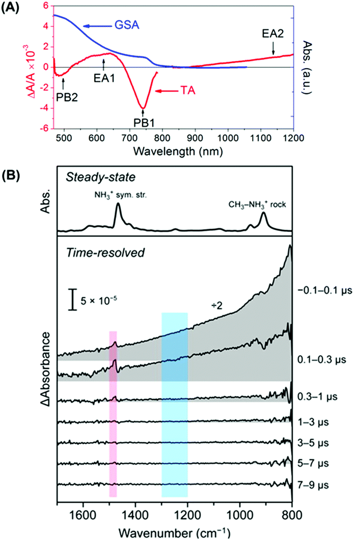 | ||
| Fig. 1 (A) Typical spectral features of a TA spectrum (red curve) of an MAPbI3 film directly after photoexcitation together with its ground-state absorption (GSA) spectrum (blue curve). (B) TA spectra in the near-IR region revealing the Fano resonances between the vibrational transitions of the MA cation and the quasi-continuous intra-CB transition (red region). Reproduced with permission: (B) from ref. 4. Copyright 2016, American Chemical Society. | ||
PB1 was correlated with the population of excited charges at the band edge. The decay time (τ) of PB1 in the MAPbI3 neat film strongly depended on the trap density of the film which varied by the synthetic methods (e.g., one-step or two-step solution and vapour deposition processes) and the resulting uniformity and crystallinity of the film. A wide range of lifetimes from hundreds of picoseconds to tens of nanoseconds can be found in the literature.5 Remarkably, a mixed-halide MAPBIxCl1−x film generally exhibited a much longer charge carrier lifetime (τ > 100 ns) because of its significantly smaller trap density.6
In well-crystalized perovskite samples where surface recombination is dominant, TA kinetics can be well fitted by a one-dimensional diffusion model to provide the diffusion coefficient (D) of photo-generated charge carriers.7 By this means, the D value was calculated to be 0.27 cm2 s−1 for MAPbBr3 single crystals. On the other hand, by applying the spatial mapping in the TA measurement, the charge transport can be followed in real space, allowing direct evaluation of D. From such TA microscopy experiments, a D value of 0.05–0.08 cm2 s−1 was achieved in an MAPbI3 thin film.8D also depended on the trap density of the perovskite and differed from the values obtained using other techniques which will be discussed in the next section.
The PL lifetimes of ∼10 ns in MAPbI3 films and >100 ns in MAPbIxCl3−x films corresponded to the decay of the charge carrier population.4–6 Modelling of the PL dynamics by one-dimensional carrier diffusion, the consequent diffusion length (LD) was estimated to be ∼100 nm for MAPbI3 polycrystalline films with D = 0.017 cm2 s−1 for electrons and 0.011 cm2 s−1 for holes.9 In mixed-halide MAPbIxCl3−x films, the LD can reach 1 μm with D = 0.04–0.05 cm2 s−1.10 The charge transport was proven to be more efficient in larger grain-sized films with D = 0.1–2.5 cm2 s−1.11 This indicates that the carrier transport in perovskites is strongly modulated by trap density—especially by the surface/interface defect states. In addition, from the D values, the mobilities of minority carriers can be evaluated to be 10−1–10−2 cm2 V−1 s−1.11
Owing to a wide variety of detection configurations—for instance, photodiodes, streak cameras, or photomultiplier tube (PMT) set ups for up-conversion or single-photon counting—with different time and spatial resolutions (e.g., in PL microscopy) together with spectral responses, TRPL is one of the most popular tools for studying charge dynamics in perovskite materials. However, some non-radiative recombination kinetics in perovskites cannot be detected in TRPL. The probed emission can also be influenced by re-absorption or photo-recycling processes.12 Therefore, the extraction of intrinsic photophysics using TRPL is always limited.
 | (1) |
 | (2) |
 | (3) |
 | ||
| Fig. 2 (A) Complex TRTS spectra of CH3NH3Pb3−xCl3 films. (B) The photoconductivity kinetics from TRTS for 2D perovskite films with different pump–probe geometries under both normal position (i.e., the sample is parallel to the incident THz field polarization, θ = 0°) and tilted angle (θ = 30°) conditions. (C) Schematic of the composition of the charge mobility to be detected by TRTS with different incident angles of THz probe pulses for two samples. (D) Typical TRMC kinetics of MAPbI3/Al2O3 films with different excitation intensities. Reproduced with permission: (A) from ref. 14. Copyright 2015, Nature Publishing Group. (B and C) From ref. 18. Copyright 2017, John Wiley & Sons, Inc. | ||
The initial charge mobility extracted immediately after photoexcitation in perovskites was processed by the above described strategies and generally fell within the 1–100 cm2 V−1 s−1 range with strong sample dependence. Taking lead iodide perovskite as an example, the mobility of an MAPbI3 neat film was 35 cm2 V−1 s−1,15 which was slightly higher than MAPbI3 embedded within mesoporous Al2O3 measured by both us (20 cm2 V−1 s−1)16 and other researchers (∼8 cm2 V−1 s−1).17 In single crystals, a much higher charge mobility of 800 cm2 V−1 s−1 was achieved.13 Such deviation of carrier mobility may result from scattering from impurities or crystal boundaries varying in the above-mentioned forms of perovskites. On the other hand, the influence of the carrier density on charge mobility should not be neglected. The inter-carrier scattering might be enhanced with high charge density, which led to reduced mobility.13
The THz field is always polarized perpendicular to the incident pulse propagation direction. Consequently, the charge mobility in TRTS reflects the carrier motion in the direction perpendicular to the THz beam. In this way, TRTS can discriminate between the contributions of the charge mobility in different spatial directions by varying the incident angle of the THz wave. Very recently, we used such angle-dependent TRTS measurements to obtain the charge mobility within different directions in emerging two-dimensional (2D) Ruddlesden–Popper perovskites (Fig. 2B and C), which are much more moisture-resistant than traditional three-dimensional (3D) perovskites.18 The angle-dependent photoconductivity in TRTS clearly manifested the preferential orientation of 2D perovskite sheets in (n-BA)2(MA)3Pb4I13 and (iso-BA)2(MA)3Pb4I13 samples.
In sum, TRTS that selectively monitors photoinduced free charge carriers with the capability of characterizing carrier mobilities is highly relevant for photovoltaic applications. It is a noncontact characterization method where the sample is not influenced by electrodes. However, it should be noted that the extraction of the charge mobilities in TRTS depends strongly on the theoretical model. In the bulk film of perovskites, the well-established Drude-like model is applicable. In nanostructured systems, however, the physically justified mathematical models for TRTS signals have yet to be fully rationalized.
 | (4) |
Given the lower frequency and longer apparatus response time, the TRMC method probes much slower timescales of dynamics than TRTS. The time-window of TRMC experiments is ns–ms, which is quite suitable for studying the charge carriers in perovskite materials (Fig. 2D). The initial TRMC measurements on the one-step prepared MAPbI3 neat film and MAPbI3 within mesoporous Al2O3 scaffolds unveiled long-lived mobile carriers with lifetimes up to 1 μs.16 The reported charge mobility (∼3 cm2 V−1 s−1) was somewhat lower than that in TRTS (∼25 cm2 V−1 s−1). Later studies revealed a strong sample dependence of the charge dynamics extracted from TRMC. In two-step fabricated MAPbI3 neat films, the TRMC mobility (∼20 cm2 V−1 s−1) is analogous to the above-mentioned one-step fabricated samples. However, a much larger imbalance between electron and hole mobilities was found with μh/μe = 30.20 A higher charge mobility of 30 cm2 V−1 s−1 was measured in MAPbIxCl3−x films with LD = 10 μm.21 This was suggested to be facilitated by the lower trap densities. In a single crystal sample, by contrast, a much longer carrier lifetime (∼15 μs) was observed with LD > 50 μm.22 This was again ascribed to a very low trap concentration, which was 2 orders of magnitude lower in single crystals than in polycrystalline films.
The main differences between the TRMC method and TRTS are the frequency and time resolution. Complementary utilization of TRTS and the TRMC method provides the charge carrier dynamics within a broader time range. However, as an indirect photoconductivity measurement, TRMC is constrained by the need for a theoretical model for data analysis, the same as TRTS.
2.2 Devices with electrodes
 | (5) |
The CELIV method is mostly employed to obtain the charge mobility of various working PSCs and qualitatively investigate the charge extraction and recombination processes. We first applied the CELIV method to investigate the transport dynamics of one-step fabricated neat MAPbI3 and MAPbI3/PCBM bilayer solar cells (Fig. 3A).23 Upon insertion of the PCBM layer, the charge mobility of MAPbI3 was doubled from 3.2 × 10⁻⁴ to 7.1 × 10⁻⁴ cm2 V−1 s−1 at room temperature.
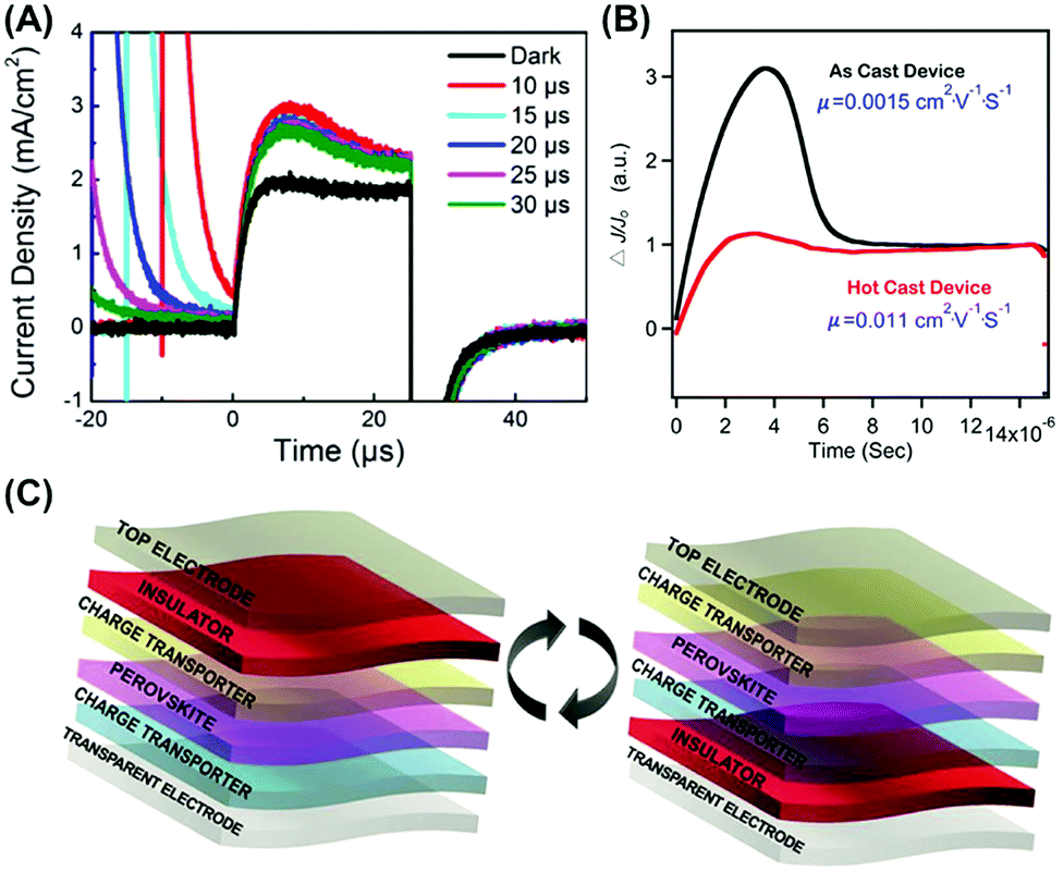 | ||
| Fig. 3 CELIV measurements of (A) a one-step fabricated neat MAPbI3 device and (B) 2D (n-BA)2(MA)3Pb4I13 devices without and with the hot casting method. (C) Device architecture of the carrier selective photo-CELIV measurement of MAPbI3. Reproduced with permission: (A) from ref. 23. Copyright 2015, American Chemical Society. (B) From ref. 25. Copyright 2016, Nature Publishing Group. (C) From ref. 27. Copyright 2017, John Wiley & Sons, Inc. | ||
The device configuration and operation conditions greatly impact the charge transport process of PSCs. Jae-Wook Kang and coworkers studied the relationship between the low-temperature transport behavior and performance of two-step fabricated MAPbI3 solar cells.24 As the temperature was cooled down from 298 to 253 K, the PCE was increased from 14.2% to 15.5% with a noticeable increase of both JSC and VOC, which was due to an increase of the CELIV mobility from 0.67 × 10⁻³ to 1.07 × 10⁻³ cm2 V−1.
Recently, the hot-cast (HC) method was employed to remarkably increase the out-of-plane crystallization of 2D (n-BA)2(MA)3Pb4I13 perovskites and hence achieved a record high PCE of 12.52% in PSCs.25 By measuring the dark-CELIV as shown in Fig. 3B, it was confirmed that the mobility of the HC device (0.011 cm2 V−1 s−1) was significantly higher than that of the room-temperature cast device (0.0015 cm2 V−1 s−1), suggestive of forming continuous charge transport channels between 2D {(MA)n−1PbnI3n+1}2− slabs and device electrodes after using the HC method. In order to further increase the out-of-plane orientation of 2D perovskites, we replaced the linear spacer cations (n-BA+) with short branched-chain ones (iso-BA+).18 As a result, (iso-BA)2(MA)3Pb4I13 solar cells exhibited a balance of hole and electron mobilities around 10−4 cm2 V−1 s−1 yet more nondispersive charge transport as compared to those based on (n-BA)2(MA)3Pb4I13.
In addition to carrier mobility measurements, CELIV can be used as a reliable and facile method to measure the capacitance and dielectric constant of perovskite based devices. For instance, Qianqian Lin et al. systematically investigated the electro-optics of MAPbI3-only planar devices.26 They employed spectroscopic ellipsometry to accurately quantify the refractive index (n) and extinction coefficient (k) of thermally evaporated MAPbI3. On the basis of these results, the real part of the static dielectric constants (ε) was determined to be ca. 70 by using the CELIV method and based on the equation ε = j0d/ε0A, where j0 is the displacement current, d is the thickness of the active layer, ε0 is the vacuum permittivity and A is the triangle voltage ramp (dU/dt).
More recently, a modified photo-CELIV method was taken to separately measure the hole and electron mobilities of perovskites by inserting a 100 nm-thick MoO3 layer in front of the selected electrodes to block the unwanted type of carrier.27 To uncover the effect of the device structure on transport dynamics, mesoporous and inverted planar MAPbI3 devices were comparatively investigated as shown in Fig. 3C. Highly balanced charge mobilities were obtained in mesoporous devices, while the hole mobility was lower than the electron mobility in planar devices by half an order of magnitude because the hole injection capability of PEDOT:PSS was inferior to that of the spiro-OMeTAD interlayer.
A unique advantage of the CELIV method is that it can probe the charge transport process directly in working PSCs. By applying both dark and light CELIV, the mobilities of intrinsic and photo-generated charge carriers can be measured, respectively. Thus, CELIV enables investigating the impact of different charge transport layers (e.g., PCBM, PEDOT:PSS, spiro-OMeTAD, TiO2, etc.) or various fabrication processes (e.g., thermal and solvent annealing, solvent additives) on carrier mobility and charge recombination. The only limitation of CELIV is that it only measures the overall charge mobility without distinguishing whether hole or electron carriers.
 | (6) |
The TOF has been demonstrated as a useful method to measure individual carrier mobility while unraveling trapping states. We initially utilized TOF to unveil the efficient and balanced charge transport in working MAPbI3 PSCs.23 The hole and electron mobilities of one-step fabricated MAPbI3/PCBM bilayer solar cells were measured to be 5.4 × 10⁻⁴ and 4.5 × 10⁻⁴ cm2 V−1 s−1, respectively, which were higher than those of devices without PCBM. Furthermore, we investigated the effects of both light soaking and phase transition on the charge transport dynamics of two-step fabricated MAPbI3 PSCs (Fig. 4A).28 It was found that both hole and electron mobilities were gradually increased upon light soaking (Fig. 4B). Meanwhile, rapid changes in hole and electron mobilities were observed during the phase transition from the tetragonal to cubic phase of perovskites.
 | ||
| Fig. 4 Schematic TOF measurements and results of (A and B) two-step fabricated MAPbI3 solar cells upon continuous light illumination and (C and D) MAPbI3 single crystal based devices. Reproduced with permission: (A and B) from ref. 28. Copyright 2016, American Chemical Society. (C and D) From ref. 30. Copyright 2015, American Association for the Advancement of Science. | ||
Apart from those of polycrystalline perovskites, the carrier mobilities of perovskite single crystals can be measured by the TOF method. A method of anti-solvent vapor-assisted crystallization was originally reported by the Bakr group to fabricate large and crack-free MAPbX3 (X = Br or I) single crystals.29 To conduct the TOF experiments, top transparent ITO and bottom MoO3/Au/Ag stack electrodes were deposited on both surfaces of perovskite single crystals, respectively. For the first time, the bulk hole mobility of MAPbBr3 single crystals was determined to be 115 cm2 V−1 s−1. Meanwhile, the Huang group reported solution-grown MAPbI3 single crystals, yielding unprecedentedly longer electron–hole diffusion lengths over 175 μm.30 By constructing the Au/MAPbI3 single crystals/PCBM:C60/Ga device as shown in Fig. 4C, the TOF electron mobility was determined to be 24.0 cm2 V−1 s−1 with negligible trap states (Fig. 4D). Note that the thickness of the Au electrode was controlled to be 25 nm to ensure both high light transparency and conductivity.
The TOF method is a powerful technique with electrode contacts to measure both hole and electron mobilities in the same device architecture, which is applicable to perovskite single crystals and polycrystalline films. Moreover, the distribution of shallow and deep traps in perovskites can be clearly differentiated by observing different plateaus in TOF j–t curves.
Enormous attention was recently paid towards how to accurately measure and effectively enhance the FET mobilities of MAPbI3 perovskites. For instance, in order to unveil the intrinsic charge transport, MAPbI3 based FETs were studied in a low temperature range of 78–198 K to eliminate the ionic transport induced screening effect (Fig. 5A).31 As the temperature was decreased below 200 K, both the hole and electron mobilities of MAPbI3 were increased by two orders of magnitude to 2.1 × 10⁻² and 7.2 × 10⁻² cm2 V−1 s−1, respectively (Fig. 5B). At room temperature or without light illumination, however, MAPbI3 FETs often exhibited poor performance with very low charge mobilities around 10−4 cm2 V−1 s−1. To solve this problem, the Ji group applied methylamine (CH3NH2) gas treatment on MAPbI3 at room temperature.32 It was found that such treated MAPbI3 displayed enlarged grain size (Fig. 5C) and hence the FET mobility was doubled to 22.75 cm2 V−1 s−1 (Fig. 5D).
 | ||
| Fig. 5 FET measurements of (A and B) MAPbI3 perovskites at different temperatures and (C and D) CH3NH2 treated MAPbI3 perovskites at room temperature. Reproduced with permission: (A and B) from ref. 31. Copyright 2015, Nature Publishing Group. (C and D) From ref. 32. Copyright 2016, American Chemical Society. | ||
Newly developed perovskite microplates also exhibited better FET performance than the polycrystalline analogues. The Duan group innovatively reported the patterned growth of regular and large arrays of MAPbI3 microplate crystals.33 By thermal annealing treatment, a transformation from n- to p-type semiconductors was clearly observed due to the degradation of perovskites. Meanwhile, these crystals showed a noticeable decrease of both charge mobility and source–drain current in FETs after thermal annealing, which was attributed to the enhanced scattering between charge carriers and defects.
FET measurements can not only measure charge mobility in the in-plane direction, but also quickly determine whether the perovskite samples are n-, p-type or ambipolar semiconductors. Unfortunately, the FET mobility is strongly dependent on the operation temperature, the grain size and even the interfacial morphology of samples. Therefore, the FET method is more applicable to perovskites with high crystallinity and purposely modified electrode surfaces in order to derive intrinsic charge mobility.
In 2013, the Hall effect measurement was applied to interpret why lead-free MASnI3 perovskites possessed the band structures of intrinsic semiconductors yet exhibited metal-like high conductivity.34 A hole concentration of 9 × 1017 cm−3 with a high Hall mobility of 200 cm2 V−1 s−1 at 250 K was observed in undoped MASnI3 single crystals (Fig. 6A and B). Moreover, the carrier concentration can be further increased by hole doping without affecting the Hall mobility. This phenomenon indicated that MASnI3 was a spontaneously doped semiconductor rather than a semimetal.
 | ||
| Fig. 6 Hall effect measurements of (A and B) MASnI3 and (C and D) MAPbBr3 single crystals. Reproduced with permission: (A and B) from ref. 34. Copyright 2013, Elsevier Inc. (C) From ref. 37. Copyright 2016, John Wiley & Sons, Inc. | ||
Lead based perovskites, however, presented much lower intrinsic carrier concentration than Sn-based perovskites. In 2014, the Huang group performed Hall effect measurements to reveal the p-type behavior of an MAPbI3 film grown by the interdiffusion method.35 Meanwhile, they observed a low hole concentration of 4–10 × 1013 cm−3, which may arise from the presence of Pb deficiency in perovskites caused by extra MAI supply during the interdiffusion process. In addition, the Hall mobility of perovskites can be reduced by 3 times after inserting the PCBM top layer.
It is worth noting that both perovskite polycrystalline films and single crystals exhibited distinctive transport behavior. To unravel the underlying physical mechanisms, the Podzorov group systematically studied the intrinsic Hall effect in vapor- and solution-grown MAPbI3 films and MAPbBr3 single crystals.36 The obtained Hall mobilities range from 0.5 to 60 cm2 V−1 s−1, which were closely correlated with the composition and crystallinity of perovskites.
In light of thermally driven phase transitions in perovskites, temperature dependent resistivity and Hall effect measurements were carried out in MAPbBr3 single crystals.37 A notable increase of conductivity by 4 orders of magnitude was achieved when the insulating perovskite single crystal was electrically biased. Such more conductive states allowed the Hall effect to be measured within 165–300 K. It was found that the Hall mobility was suddenly doubled at 235 K when the cubic phase was transited to the tetragonal phase (Fig. 6C). This result was well consistent with the rapid switch of TOF hole and electron mobilities during the same phase transition in MAPbI3 solar cells.28
The Hall effect technique is an all-round steady-state method to simultaneously acquire the bulk charge mobility, free carrier density, electrical conductivity and diffusion length of both perovskite films and single crystals. Meanwhile, the doping effect of perovskites with different chemical compositions can also be examined by this method. However, because of the equipment limitations, the Hall effect technique usually cannot measure those materials with low conductivity.
The current-density versus voltage (J–V) curve measured by the SCLC method is often divided into three regimes: (1) a linear ohmic regime to calculate the electrical conductivity (σ) at low bias, (2) a trap-filled regime to estimate the trap density at middle bias, and (3) a trap-free SCLC regime to determine the charge mobility at high bias. The SCLC mobility can be calculated using eqn (7):
 | (7) |
The SCLC technique was mostly applied to investigate the various electronic properties of perovskite single crystals fabricated by different methods. Large SCLC hole and electron mobilities of 164 and 24.8 cm2 V−1 s−1 were achieved in solution-grown MAPbI3 single crystals, respectively.30 The Bakr group also conducted the SCLC measurement to yield equivalently low trap densities of 5.8 × 10⁹ and 3.3 × 1010 cm−3 in MAPbBr3 and MAPbI3 single crystals, respectively, which were grown by the anti-solvent vapor-assisted method (Fig. 7A and B).29 The SCLC mobility of the MAPbBr3 single crystals (38 cm2 V−1 s−1) was found an order of magnitude higher than the MAPbI3 analogues (2.5 cm2 V−1 s−1).
 | ||
| Fig. 7 SCLC measurements of (A) MAPbBr3 and (B) MAPbI3 single crystals grown by an anti-solvent vapor-assisted method, and (C and D) MAPbBr3 planar-integrated single-crystals. Reproduced with permission: (A and B) from ref. 29. Copyright 2015, American Association for the Advancement of Science. (C and D) From ref. 39. Copyright 2015, Nature Publishing Group. | ||
The SCLC method can also be utilized to investigate the impact of phase transition on the transport properties of perovskite single crystals. For example, the Yang group unveiled the distinct transport dynamics of the black α-phase (perovskite-type) and yellow δ-phase (non-perovskite type) of FAPbI3 single crystals grown by the liquid-based crystallization method.38 By using SCLC measurements, a higher charge mobility (4.4 cm2 V−1 s−1) and electrical conductivity (1.1 × 10⁻⁷ Ω−1 cm−1) yet a lower defect concentration (6.2 × 1011 cm−3) and free carrier (1.5 × 1011 cm−3) density can be obtained in the α-phase FAPbI3 single crystals than the δ-phase analogues.
However, all these above bulk perovskite single crystals are not suitable for practical device applications due to the absence of a substrate or undesirably large crystal size. In an early attempt, the Sargent and Bakr groups directly grew MAPbBr3 single crystals on substrates to obtain highly crystalline films, which were termed planar-integrated single-crystal (ISC) perovskites (Fig. 7C).39 By combination of the Hall effect and SCLC techniques, an ultrahigh charge mobility of 60 cm2 V−1 s−1, a low trap density of 2 × 1011 cm−3 and a high conductivity of 2 × 10⁻⁸ Ω−1 cm−1 were achieved (Fig. 7D). These results suggested that the electrical properties of ISC perovskites nearly approached those of free-standing single crystals and were much better than those of solution-processed or vapor-deposited polycrystalline films.
Therefore, SCLC is a commonly used method to determine the hole and electron mobilities of perovskites in different device architectures. Both electrical conductivity and defect densities can be simultaneously obtained by simply scanning I–V curves in the dark. It is worth noting that the SCLC method is only applicable to perovskites with intrinsic charge densities lower than 1014 cm−3, and therefore it is more suitable for the measurement of perovskite single crystals.
2.3 Summary
To provide an overview instruction on the selection of the technique to investigate the photo-physics in perovskite materials, we summarize the technical parameters, functionality and limitation of each above-mentioned method in Table 1. Here the time scale of the detection and the charge density needed during the measurement limit the scope of each technique for photo-physical studies. An in-depth discussion on the comparison of these techniques during the studies of photo-physics in perovskite materials will be presented in Section 4.| Method | Excitation pulse (s) | Probe window (s) | Charge densityo (cm−3) | Output | Sample requirement and advantage | Main limitations |
|---|---|---|---|---|---|---|
| a Optical delay line. b Electric trigger. c Differential absorption. d Excited state lifetime. e Emissive state lifetime. f Free charge concentration. g Charge carrier mobility. h Free charge lifetime. i Charge mobility in the out-of-plane direction. j Electrical conductivity. k Trap density. l Bulk charge mobility. m Diffusion length. n Charge mobility in the in-plane direction. o Charge density in pump–probe measurements (TA, TRPL, TRTS, TRMC, CELIV, TOF) is calculated as the multiplication of the excitation concentration per pulse and the absorption cross section of perovskites (105 cm−1 for MAPbI3), while for steady-state measurements it is defined as the charge carrier concentration during the measurement. | ||||||
| TA | 10−14–10−13 |
10−13–10−8![[thin space (1/6-em)]](https://www.rsc.org/images/entities/char_2009.gif) a a
10−11–10−4 |
1018–1020 | ΔAbs,cτ1d | No contact electrode, transparent (OD < 1) | Overlap of different spectral components |
| TRPL | 10−13–10−10 | 10−12–10−4 | 1015–1017 | τ 2 | No contact electrode, emissive sample | Only probing the emissive state |
| TRTS | 10−14–10−13 | 10−12–10−9 | 1018–1020 | n,fμg | No contact electrode, specific substrate (e.g., quartz) | Only sensitive to free charges, need theoretical model for data analysis |
| TRMC | 10−13–10−10 | 10−10–10−4 | 1018–1020 | n, μ, τ3 | No contact electrode, specific substrate (e.g., quartz) | Only sensitive to free charges, need theoretical model for data analysis |
| CELIV | 10−9–10−5 | 10−9–10−6 | 1015–1017 | μ out | Both contact electrodes, two injection-blocking layers, applicable to working solar cells | Cannot distinguish the type of charge carrier |
| TOF | 10−9–10−8 | 10−9–10−6 | 1014–1015 | μ out | Both contact electrodes (one must be transparent), two injection-blocking layers, measure hole and electron mobilities in the same device | Thick film (>500 nm), cannot measure in the dark |
| SCLC | Steady-state method | 1010–1016 | μ out, σ,jntrapk | Both contact electrodes, measure hole and electron mobilities in different devices | Low intrinsic charge density (<1014 cm−3) | |
| HALL | μ bulk,ln, σ, Dm | Both contact electrodes, measure bulk charge mobility, distinguish whether n- or p-type | High electrical conductivity (>10−9 S) | |||
| FET | μ in | Both contact electrodes, distinguish whether n- or p-type | High film quality to observe the obvious field effect | |||
3. Charge carrier dynamics of perovskites
Based on these transient and steady-state measurements as discussed above, we now present an in-depth summary of the featured charge carrier dynamics of perovskites in thin films and solar cells, respectively.3.1 Neat films
The exciton binding energy of lead halide perovskites, especially MAPbI3, was found to be less than the thermal activation energy kbT = 14–25 meV by various measurements. Consequently, the photo-generated excitons spontaneously dissociated via thermal activation. The kinetics of the photo-generated carrier concentration are determined by a combination of the first-order trap-state mediated charge recombination (A), the second-order non-geminate free carrier recombination (B), and the three-body Auger recombination (C) using eqn (8): | (8) |
 | ||
| Fig. 8 (A) Dependence of PL0 and PL kinetics on the excitation density in MAPbBr3 crystals illustrating the recombination mode for the photo-generated charges. PL lifetimes for MAPbX3 polycrystalline films with different (B) grain sizes, (C) halide compositions, and (D) interfacial conditions. Reproduced with permission: (B) from ref. 42. Copyright 2014, American Chemical Society. (C) From ref. 43. Copyright 2014, The Royal Society of Chemistry. (D) From ref. 44. Copyright 2014, The Royal Society of Chemistry. | ||
Therefore, the photovoltaic charge transport parameters revealed by spectroscopic studies are strongly influenced by the trap states. The dependences of trap densities on the PL lifetime have been systematically investigated (Fig. 8B–D). This includes (1) grain size (the PL lifetime of the MAPbI3 polycrystalline films increased from 2 ns to 100 ns with an increment of grain sizes from <250 nm to >1 μm),42 (2) chemical composition (the PL lifetime varied from 100 ns to 446 ns in MAPbBr3−xClx films),43 and (3) interfacial phenomena (the metal oxide/perovskite interfaces, for instance, would change the intrinsic PL lifetime of the neat perovskite film).44
Early studies by using TA disclosed the so-called hot-phonon bottleneck due to the substantial carrier re-absorption of optical phonons by carriers, which induces the slowing down in the cooling rate of hot charges in MAPbI3 perovskites at high carrier densities.40 Such a hot-phonon bottleneck is commonly observed in inorganic semiconductors, yet found to be much more pronounced in perovskites. This can be attributed to the decoupling between electrons and optical phonons due to the independent motion of organic cations or internal ferroelectricity in perovskites.
Recent studies showed that even in the low carrier density regime (<1017 cm−3) far below the hot-phonon bottleneck regime, the slow hot charge cooling was still valid as evidenced by a long-lived (∼100 ps) hot emission in single-crystal MAPbBr3 and FAPbBr3 microplates (Fig. 9A).45 Such hot charges even transport in perovskites within a long distance (∼230 nm) observed by ultrafast TA microscopy (Fig. 9B).46 The formation of long-range polarons where photo-generated charge carriers caused by long-range lattice deformation was considered as one of the main origins. After photoexcitation, the interaction between the photogenerated charges and ionic lattices of the perovskite would induce long-range lattice deformation. Consequently, charges would be self-trapped within the lattice as polarons. The lattice deformation would screen the Coulombic interaction which is responsible for the scattering between charges and LO phonons. This would lead to a drastically reduced hot carrier cooling.
 | ||
| Fig. 9 (A) Hot emission observed in TRPL in single-crystal MAPbBr3 microplates with a 100 ps lifetime. (B) TA microscopy images of the MAPbI3 film probing the band edge carriers (excited at 1.97 eV) and hot carriers (excited at 3.14 eV). Reproduced with permission: (A) from ref. 45. Copyright 2016, American Association for the Advancement of Science. (B) from ref. 46. Copyright 2017, American Association for the Advancement of Science. | ||
3.2 Bilayer films
Beyond neat films, perovskite materials need to be attached to charge (electron or hole) acceptors such as TiO2, PCBM, spiro-OMeTAD and NiO to separate the photo-generated charges, which is essential for working solar cells. The charge transfer process between the perovskites and these acceptors can be visualized using different spectroscopic techniques.Firstly, the additional depopulation pathway can be induced for excited states resulting in faster decay kinetics of the band edge bleaching PB1 in TA.9 However, unexpected slower charge transfer times (>100 ps) were observed for perovskite/acceptor bilayer films using the TA technique those that of conventional photovoltaic materials (e.g., organic dyes, QDs, or semiconducting polymers) where the charge injection occurred within the sub-ps timescale. Further studies showed that the TA kinetics in perovskite/acceptor systems actually represented diffusion-coupled charge transfer processes where charge diffusion in perovskite occurred before interfacial charge transfer, where the timescale ranged from 200 ps to ns. Leng et al. summarized the TA kinetics of perovskite/acceptor systems with various thicknesses of perovskites and extracted the electron transfer time to PCBM as 6 ps and the hole transfer time to spiro-OMeTAD as 8 ps (Fig. 10).47 The long LD prior to interfacial charge transfer can also be proven in TA in the IR range where the appearance of free charges in the acceptors can be identified as a broad IR absorption spectrum.
 | ||
| Fig. 10 Schematic illustrating charge dynamics in perovskites attached to the charge acceptor in the device configuration. Reproduced with permission from ref. 4. Copyright 2016, American Chemical Society. | ||
Secondly, distinct charge mobilities between perovskite and charge acceptors pave the way for monitoring charge transfer dynamics in perovskite/acceptor systems by TRTS. Our studies of MAPbI3/mesoporous TiO2 layers unraveled that electron injection processes were complete within 10 ps.16 This was identified by a decrease of the initial charge mobility directly after photo-excitation in comparison to the neat perovskite in TRTS signals which featured the prompt depopulation of one species of charges either electrons or holes after charge transfer. From those studies, electron and hole mobilities can also be distinguished by considering that the TRTS mobility is a sum of both parts in the system, while the carrier mobility in the acceptors is usually orders of magnitudes lower than that in the perovskites which can be neglected in TRTS spectra. The electron mobility revealed for an MAPbI3 film was comparable to or slightly higher than the hole mobility with μe/μh = 1–2, which demonstrated balanced charge transport.16
3.3 Working solar cells
As perovskites are organic–inorganic hybrid materials with strong light and thermal sensitivity, there remain two long-term queries about perovskite solar cells. One is why light illumination and thermally induced phase transition have a great influence on the charge transport dynamics and thus the cell performance of perovskites. The other is whether the transport properties of perovskite photovoltaics resemble those of organic or inorganic devices. In other words, it is necessary to verify whether dispersive or nondispersive charge transport, hopping or band-like conduction dominates in perovskite devices. To answer these two questions, here we not only systematically discuss the impacts of trap states and phase transition on the transport properties, but also highlight the nondispersive charge transport and band-like conduction of perovskite devices with electrodes.Although perovskites were reported to exhibit a large tolerance of trap states, we have to admit that the existence of shallow traps hinders the charge transport of PSCs. Our TOF studies of MAPbI3 solar cells discovered the existence of trap-assisted recombination and direct shallow trap filling process with gradually increased hole and electron mobilities upon light soaking (Fig. 11A and B).28 A similar conclusion was drawn by another modified CELIV measurement.26 It was found that in both planar and mesoporous MAPbI3 devices all the remaining trapped carriers disappeared after a photogeneration–extraction sequence, which suggested the absence of deep traps in perovskites.
 | ||
| Fig. 11 Light illumination time dependent (A) TOF measurements of perovskite solar cells and (B) schematic mechanism of the trap filling process upon light soaking. Temperature dependent (C) TOF and conductivity measurements of perovskite solar cells and (D) schematic transport dynamics influenced by phase transition. Reproduced with permission: (A–D) from ref. 28. Copyright 2016, American Chemical Society. | ||
Meanwhile, PCBM was widely reported to play an important role in passivating the interfacial trap states of perovskites. Despite that a few shallow traps were unavoidably left at the interface between MAPbI3 and PCBM, the existence of PCBM intercalation often led to faster charge separation with suppressed recombination and hence higher mobility.23 By Hall effect measurements, the PCBM layer was also found to efficiently passivate the traps of MAPbI3 films, yielding a reduction of the intrinsic hole concentration and an increase of the Hall mobility of perovskites both by 3 times.35
Compared to polycrystalline films, perovskite single crystals often exhibited much lower trap densities. For instance, MAPbX3 (X = Br or I) single crystals showed low conductivities around 108 S cm−1 and extremely low trap-state densities of 109–1010 cm−3.29 By contrast, the conductivity of FAPbI3 single crystals was an order of magnitude higher, which was mainly attributable to the greatly increased carrier density caused by the lower bandgap of FAPbI3.38 On the other hand, owing to the self-doping effect, MASnI3 exhibited metal-like high conductivity with a much higher intrinsic carrier concentration of 9 × 1017 cm−3 than MAPbI3.34 This indicated enormous trap states in Sn-based perovskites, which needed to be largely suppressed in order to enhance their photovoltaic performance.
More importantly, it was found that the charge transport behaviors of perovskites resembled those of inorganic semiconductors. With the aid of Hall effect measurements, carrier lifetimes and diffusion lengths were measured to be 30 ms (2.7 ms) and 23 nm (650 nm) in MAPbI3 polycrystalline films and MAPbBr3 single crystals, respectively, indicative of much weaker charge trapping in perovskites than most high-purity crystalline inorganic semiconductors.36 As a result, better charge transport properties can be achieved in perovskite single crystals than polycrystalline perovskites.29,30 Likewise, by utilizing the SCLC method, five orders of magnitude lower hole and electron trap densities were attained in MAPbI3 single crystals than in MAPbI3 polycrystalline films.30
On the one hand, a sudden change in charge mobility often occurred during the phase transition process. Our group utilized temperature dependent TOF in MAPbI3/PCBM bilayer solar cells and observed rapid changes in both hole and electron mobilities when the perovskite phase change from tetragonal to cubic crystalline structures was observed (Fig. 11C and D).28 Balanced charge transport and unchanged electrical conductivity were finally achieved during phase transition at 310–330 K, resulting in the highest PCE. A similar phenomenon was observed in the Hall measurement of MAPbBr3 single crystals.37 When the cubic phase was transited to the tetragonal phase, the Hall mobility was suddenly doubled at 235 K. It was disclosed that charge transport in the cubic phase was limited by acoustic phonon scattering rather than impurity scattering, while reduced electron–phonon scattering was achieved in the tetragonal phase owing to the suppressed rotation of the MA dipoles.
On the other hand, different perovskite phases often exhibited distinct transport properties. By SCLC measurements, it was found that higher charge mobility yet lower defect densities can be obtained in α-phase FAPbI3 single crystals than Δ-phase analogues.38 This finding explained well why only α-phase FAPbI3 based solar cells afforded high PCE. By the FET method, the thermal transformation of MAPbI3 microplate crystals from n-type to ambipolar and finally to p-type semiconductor behavior was clearly observed, owing to the corresponding slight disintegration of MAPbI3.33
Our recent studies directly confirmed the nondispersive charge transport in MAPbI3/PCBM bilayer solar cells at room temperature by observing a distinct plateau in both hole and electron TOF measurements (Fig. 11A).28 This was distinctive from the dispersive transport among most organic solar cells, which originated often from the existence of disordered structures and deep-level traps. This result also well explained why perovskite solar cells outperformed organic counterparts, owing to the high crystallinity and large tolerance of trap states in perovskites. Similarly, by modified photo-CELIV, nondispersive electron transport was also observed in planar MAPbI3 solar cells caused by the passivating function of PCBM, while dispersive electron transport was clearly observed in mesoporous perovskite devices due to the presence of traps at the TiO2/MAPbI3 interface.27 This work further emphasized the importance of the PCBM layer in achieving a nondispersive nature in perovskite devices.
In the absence of the PCBM layer, by contrast, nondispersive charge transport can still be achieved by lowering the operating temperature. The conversion from dispersive to nondispersive charge transport at low temperature was unraveled by CELIV measurements of MAPbI3/spiro-OMeTAD bilayer solar cells.24 This behavior resulted from the suppressed trap states caused by the disordered MA dipoles at low temperature.
As organic–inorganic hybrid materials, there also remains an uncertainty about whether hopping or band-like conduction dominates in PSCs. We found that the conduction pathway was determined by not only the perovskite phases, but also the fabrication process. For instance, we unveiled that hopping and band-like conduction individually dominated in the tetragonal and cubic phases of perovskites by applying the TOF method in two-step fabricated MAPbI3 solar cells (Fig. 12A).28 By contrast, in one-step fabricated MAPbI3 solar cells, the charge mobility was gradually decreased with increasing temperature by utilizing temperature-dependent CELIV, indicative of the band-like conduction in perovskites (Fig. 12B).23 By the Hall effect measurement for MAPbBr3 single crystals, a band-like transport was also verified by observing higher charge mobility at lower temperature (Fig. 12C).37 These results indicated that the conduction type was also related to the fabrication process.
 | ||
| Fig. 12 Temperature dependent (A) TOF measurements of two-step fabricated MAPbI3 solar cells, (B) CELIV measurements of one-step fabricated MAPbI3 solar cells, and (C) Hall effect measurements of MAPbBr3 single crystals. Reproduced with permission: (A) from ref. 28. Copyright 2016, American Chemical Society. (B) From ref. 23. Copyright 2015, American Chemical Society. (C) From ref. 37. Copyright 2016, John Wiley & Sons, Inc. | ||
In addition, extremely low bimolecular recombination coefficients of 10−11–10−10 cm3 s−1 were found for vapor- and solution-grown MAPbI3 films and MAPbBr3 single crystals, which were comparable to those of the best direct-band inorganic semiconductors.36 In addition, two orders of magnitude higher charge mobilities were observed in MAPbI3 based FETs when the temperature was decreased below 200 K, suggesting phonon scattering-limited transport, which is similar to that of common inorganic semiconductors.31 Therefore, all these reports verified the fact that perovskites prefer to exhibit the properties of inorganic semiconductors such as GaAs rather than the organic ones.
4. Comparison of transportation methods
Although the above-mentioned techniques are all self-consistent in elucidating the photophysics in perovskite materials individually, the comparison among those techniques exhibits a large deviation. The most critical discrepancy stems from the values of carrier mobility as measured using different transportation methods, which cover a wide range of 8 orders of magnitude as summarized in Fig. 13A (see Table S1 in the ESI†). Generally speaking, the charge carrier mobilities in perovskites are dominated by intrinsic carrier–lattice interaction and extrinsic carrier-imperfection interaction of the materials. The former is dominated by the intrinsic electronic structures of the perovskites, while the latter reflects the charge carrier scattering by grain boundaries, dopants, lattice defects, etc. Putting aside the effect of sample variations including structures, morphologies, trap densities, etc., which are also reported to regulate the carrier mobility by one to two orders of magnitude, we can still classify the results obtained using different techniques into two categories—mobilities extracted using the CELIV and TOF methods are usually below the level of 10−2 cm2 V−1 s−1, while the values measured using the other methods are orders of magnitude higher. Interestingly, we found that the mobilities of perovskite single crystals that were expected to be relatively defect-free, when measured in TOF, were within the same range as provided by the other methods (Fig. 13A). This indicates that the CELIV and TOF techniques are more sensitive to the long-range order of perovskites with significant contribution from the grain boundaries or interface phenomena. In contrast, other time-resolved or steady-state approaches are focused more on the local information of charge carriers. | ||
| Fig. 13 (A) Charge carrier mobilities of perovskite films and single crystals measured by various techniques, (B) schematic illustrating the main detection regime of those techniques with different time windows, (C) dependence of the probing time-scale and (D) light excitation intensities on the charge mobilities obtained using different techniques for MAPbIxCl3−x films. | ||
Recent research efforts on the grain-size dependent mobilities in TRMC have already put forward similar concerns that the time scale of diffusive transport across grain boundaries in perovskites is much slower than the period of the microwave field (100 ps) which cannot be fully characterized.48 In other words, pump–probe methods such as TRTS and TRMC tend to reflect the intrinsic capabilities of the charge transport dominated by the local acoustic photon scattering or electron–phonon scattering. In contrast, methods like CELIV and TOF with contact electrodes characterize charge carriers that undergo the entire transport period across the film structure within a much longer time scale of ns–μs (Fig. 13B). In this regard, the carrier-defect scattering, as a bottleneck for charge transport, may dominate the characteristic charge mobilities. We consider it as one of the major origins for the deviation of charge mobilities obtained from those different methods. To further support this conclusion, we summarize the dependence of charge mobilities in MAPbIxCl3−x polycrystalline films on the probing time-scale (defined as the time duration of the probe pulse) measured via different methods in the literature (Fig. 13C). An evident decrease of mobilities accompanied by an increase of the probing time-scale can be observed, which is consistent with our assumption. It should also be noted that in steady-state measurements (SCLC and Hall effect), the inter-grain and cross-grain transportation of charge carriers can be well distinguished by modulating the applied voltage or magnetic field. Therefore, the charge mobilities extracted using those methods can still be close to those obtained using the TRTS and TRMC methods.
Another crucial factor to be accounted for is the photo-excitation intensities, which also determine the carrier concentration in perovskites. According to classic semiconductor physics, the carrier mobility is reverse to the charge scattering rates (γ). In principle, γ would increase as a function of the carrier concentration in a semiconductor due to the increased carrier–carrier scattering, which leads to a reduction of charge mobility.49 However, the summarized dependences between excitation intensities and mobilities measured via various techniques for perovskite materials exhibit the opposite trend (Fig. 13D). One plausible explanation is the dynamic trap filling process at high carrier densities, which diminishes the carrier–defect scattering of residual free carriers. Such trap filling has been widely observed in perovskite materials, indicating that the carrier concentration not only mediates the recombination mode of the photo-generated charges (i.e., first-order or higher-order charge recombination) but also determines the effective defect densities at excited states.50
Besides that, the analysis methodologies of each technique would also result in a deviation of the output. As mentioned above, for instance, the analysis of AC conductivity in TRTS and TRMC required comprehensive physical models which may vary by the geometries of the samples and the experimental configurations. In addition, the possible lattice deformation at excited states by polaron formation or photo-induced ferroelectricity could also lead to different charge carrier dynamics measured between the dark state methods (e.g., FET, Hall effect) and the methods with light excitation.
There remains a long-standing debate concerning which method is more appropriate to rationalize the photo-physical origins of the superior photovoltaic performance of perovskite materials. The above comparisons suggest that various steady-state, transient and ultrafast techniques are indeed complementary to each other, at least in determining carrier mobilities. In brief, the capability of transporting photo-generated charge carriers is dominated by several scattering processes including (1) carrier–phonon, (2) carrier–carrier, (3) carrier–plasmon, and (4) carrier–impurity scattering. Different techniques presented in this review only characterize some of those processes depending on the above-mentioned transport parameters. Therefore, it is a risk to interpret the charge dynamics of perovskites by using one single technique without specifying the detection regime. In order to characterize the entire charge transport process within perovskites from charge photo-generation, separation to collection, a combination of multiple approaches is highly needed.
5. Conclusions
This review systematically introduced the charge transport dynamics of perovskites, which were investigated using various techniques including ultrafast spectroscopies (TA, TRPL, TRTS, TRMC), transient electrical measurements (CELIV, TOF), and steady-state methods (FET, Hall effect, SCLC). Followed by a brief introduction of each technique, we summarized representative results of perovskites in the literature obtained from those transportation methods in terms of carrier mobilities, lifetimes, diffusion lengths, etc. From these results, most of the critical charge carrier dynamics are gained in neat films, bilayer films and operating solar cells based on perovskites. In neat films, photo-generated species are predominantly contributed by free carriers which mainly undergo trap-assisted first-order recombination. In conjunction with the charge acceptor to form the bilayer films, the interfacial charge transfer is generally efficient within the picosecond time-scale. In real device configurations, the charge transport is non-dispersive and dominated by the band-like conduction which also exhibits large trap tolerance.More importantly, we manifested the difference and limitation of each technique in the photo-physical studies of perovskite materials. We showed that due to various time windows and excitation levels, these techniques are sensitive to specific processes during charge transport. Ultrafast spectroscopies with high excitation concentrations and relatively short time-windows tend to probe the local charge carrier dynamics that are determined by the intrinsic structures of the perovskites, while transient electrical measurements with long time-windows and low excitation intensities detect the collective charge transport behaviors with large contribution from the grain boundaries and interface phenomena within the perovskites. We also emphasize the complementary points of view that integrate the different techniques to rationalize the solar cell performance using photo-physical studies.
Acknowledgements
Z. L. thanks the support from the National Natural Science Foundation of China (NSFC) under grant no. 51473036. K. Z. and T. P. acknowledges the support from the Swedish Research Council, the KAW Foundation, the NPRP grant #NPRP7-227-1-034 obtained from the Qatar National Research Fund (a member of the Qatar Foundation), and the STINT grant #CH2015-6232 from the Swedish Foundation for International Cooperation in Research and Higher Education.Notes and references
- Best Research Cell Efficiencies: http://www.nrel.gov/ncpv/images/efficiency_chart.jpg, accessed in March 2017.
- T. C. Sum, N. Mathews, G. Xing, S. S. Lim, W. K. Chong, D. Giovanni and H. A. Dewi, Acc. Chem. Res., 2016, 49, 294–302 CrossRef CAS PubMed.
- X. Wu, M. T. Trinh, D. Niesner, H. Zhu, Z. Norman, J. S. Owen, O. Yaffe, B. J. Kudisch and X.-Y. Zhu, J. Am. Chem. Soc., 2015, 137, 2089–2096 CrossRef CAS PubMed.
- S. Narra, C.-C. Chung, E. W.-G. Diau and S. Shigeto, J. Phys. Chem. Lett., 2016, 7, 2450–2455 CrossRef CAS PubMed.
- K. G. Stamplecoskie, J. S. Manser and P. V. Kamat, Energy Environ. Sci., 2015, 8, 208–215 CAS.
- S. D. Stranks, G. E. Eperon, G. Grancini, C. Menelaou, M. J. P. Alcocer, T. Leijtens, L. M. Herz, A. Petrozza and H. J. Snaith, Science, 2013, 342, 341–344 CrossRef CAS PubMed.
- Y. Yang, Y. Yan, M. Yang, S. Choi, K. Zhu, J. M. Luther and M. C. Beard, Nat. Commun., 2015, 6, 7961 CrossRef CAS PubMed.
- Z. Guo, J. S. Manser, Y. Wan, P. V. Kamat and L. Huang, Nat. Commun., 2015, 6, 7471 CrossRef CAS PubMed.
- G. Xing, N. Mathews, S. Sun, S. S. Lim, Y. M. Lam, M. Grätzel, S. Mhaisalkar and T. C. Sum, Science, 2013, 342, 344–347 CrossRef CAS PubMed.
- M. Saba, M. Cadelano, D. Marongiu, F. Chen, V. Sarritzu, N. Sestu, C. Figus, M. Aresti, R. Piras, A. G. Lehmann, C. Cannas, A. Musinu, F. Quochi, A. Mura and G. Bongiovanni, Nat. Commun., 2014, 5, 5049 CrossRef CAS PubMed.
- J.-C. Blancon, W. Nie, A. J. Neukirch, G. Gupta, S. Tretiak, L. Cognet, A. D. Mohite and J. J. Crochet, Adv. Funct. Mater., 2016, 26, 4283–4292 CrossRef CAS.
- L. M. Pazos-Outón, M. Szumilo, R. Lamboll, J. M. Richter, M. Crespo-Quesada, M. Abdi-Jalebi, H. J. Beeson, M. Vrućinić, M. Alsari, H. J. Snaith, B. Ehrler, R. H. Friend and F. Deschler, Science, 2016, 351, 1430–1433 CrossRef PubMed.
- D. A. Valverde-Chávez, C. S. Ponseca, C. C. Stoumpos, A. Yartsev, M. G. Kanatzidis, V. Sundström and D. G. Cooke, Energy Environ. Sci., 2015, 8, 3700–3707 Search PubMed.
- C. La-o-vorakiat, T. Salim, J. Kadro, M.-T. Khuc, R. Haselsberger, L. Cheng, H. Xia, G. G. Gurzadyan, H. Su, Y. M. Lam, R. A. Marcus, M.-E. Michel-Beyerle and E. E. M. Chia, Nat. Commun., 2015, 6, 7903 CrossRef CAS PubMed.
- R. L. Milot, G. E. Eperon, H. J. Snaith, M. B. Johnston and L. M. Herz, Adv. Funct. Mater., 2015, 25, 6218–6227 CrossRef CAS.
- C. S. Ponseca, T. J. Savenije, M. Abdellah, K. Zheng, A. Yartsev, T. R. Pascher, T. Harlang, P. Chabera, T. Pullerits, A. Stepanov, J.-P. Wolf and V. Sundström, J. Am. Chem. Soc., 2014, 136, 5189–5192 CrossRef CAS PubMed.
- C. Wehrenfennig, G. E. Eperon, M. B. Johnston, H. J. Snaith and L. M. Herz, Adv. Mater., 2014, 26, 1584–1589 CrossRef CAS PubMed.
- Y. Chen, Y. Sun, J. Peng, W. Zhang, X. Su, K. Zheng, T. Pullerits and Z. Liang, Adv. Energy Mater., 2017, 1700162 CrossRef.
- C. Colbeau-Justin and M. A. Valenzuela, Rev. Mex. Fis., 2013, 59, 191–200 CAS.
- H. Oga, A. Saeki, Y. Ogomi, S. Hayase and S. Seki, J. Am. Chem. Soc., 2014, 136, 13818–13825 CrossRef CAS PubMed.
- E. M. Hutter, G. E. Eperon, S. D. Stranks and T. J. Savenije, J. Phys. Chem. Lett., 2015, 6, 3082–3090 CrossRef CAS PubMed.
- Y. Bi, E. M. Hutter, Y. Fang, Q. Dong, J. Huang and T. J. Savenije, J. Phys. Chem. Lett., 2016, 7, 923–929 CrossRef CAS PubMed.
- Y. Chen, J. Peng, D. Su, X. Chen and Z. Liang, ACS Appl. Mater. Interfaces, 2015, 7, 4471–4475 CAS.
- R. T. Ginting, E.-S. Jung, M.-K. Jeon, W.-Y. Jin, M. Song and J.-W. Kang, Nano Energy, 2016, 27, 569–576 CrossRef CAS.
- H. Tsai, W. Nie, J.-C. Blancon, C. C. Stoumpos, R. Asadpour, B. Harutyunyan, A. J. Neukirch, R. Verduzco, J. J. Crochet, S. Tretiak, L. Pedesseau, J. Even, M. A. Alam, G. Gupta, J. Lou, P. M. Ajayan, M. J. Bedzyk, M. G. Kanatzidis and A. D. Mohite, Nature, 2016, 536, 312–316 CrossRef CAS PubMed.
- Q. Lin, A. Armin, R. C. R. Nagiri, P. L. Burn and P. Meredith, Nat. Photonics, 2015, 9, 106–112 CrossRef CAS.
- M. Petrović, T. Ye, C. Vijila and S. Ramakrishna, Adv. Energy Mater., 2017, 1602610 CrossRef.
- J. Peng, Y. Sun, Y. Chen, Y. Yao and Z. Liang, ACS Energy Lett., 2016, 1, 1000–1006 CrossRef CAS.
- D. Shi, V. Adinolfi, R. Comin, M. Yuan, E. Alarousu, A. Buin, Y. Chen, S. Hoogland, A. Rothenberger, K. Katsiev, Y. Losovyj, X. Zhang, P. A. Dowben, O. F. Mohammed, E. H. Sargent and O. M. Bakr, Science, 2015, 347, 519–522 CrossRef CAS PubMed.
- Q. Dong, Y. Fang, Y. Shao, P. Mulligan, J. Qiu, L. Cao and J. Huang, Science, 2015, 347, 967–970 CrossRef CAS PubMed.
- X. Y. Chin, D. Cortecchia, J. Yin, A. Bruno and C. Soci, Nat. Commun., 2015, 6, 7383 CrossRef CAS PubMed.
- M.-J. Zhang, N. Wang, S.-P. Pang, Q. Lv, C.-S. Huang, Z.-M. Zhou and F.-X. Ji, ACS Appl. Mater. Interfaces, 2016, 8, 31413–31418 CAS.
- D. Li, H.-C. Cheng, Y. Wang, Z. Zhao, G. Wang, H. Wu, Q. He, Y. Huang and X. Duan, Adv. Mater., 2016, 29, 1601959 CrossRef PubMed.
- Y. Takahashi, H. Hasegawa, Y. Takahashi and T. Inabe, J. Solid State Chem., 2013, 205, 39–43 CrossRef CAS.
- Z. Xiao, C. Bi, Y. Shao, Q. Dong, Q. Wang, Y. Yuan, C. Wang, Y. Gao and J. Huang, Energy Environ. Sci., 2014, 7, 2619–2623 CAS.
- Y. Chen, H. T. Yi, X. Wu, R. Haroldson, Y. N. Gartstein, Y. I. Rodionov, K. S. Tikhonov, A. Zakhidov, X.-Y. Zhu and V. Podzorov, Nat. Commun., 2016, 7, 12253 CrossRef CAS PubMed.
- H. T. Yi, X. Wu, X. Zhu and V. Podzorov, Adv. Mater., 2016, 28, 6509–6514 CrossRef CAS PubMed.
- Q. Han, S.-H. Bae, P. Sun, Y.-T. Hsieh, Y. M. Yang, Y. S. Rim, H. Zhao, Q. Chen, W. Shi, G. Li and Y. Yang, Adv. Mater., 2016, 28, 2253–2258 CrossRef CAS PubMed.
- M. I. Saidaminov, V. Adinolfi, R. Comin, A. L. Abdelhady, W. Peng, I. Dursun, M. Yuan, S. Hoogland, E. H. Sargent and O. M. Bakr, Nat. Commun., 2015, 6, 8724 CrossRef CAS PubMed.
- M. B. Price, J. Butkus, T. C. Jellicoe, A. Sadhanala, A. Briane, J. E. Halpert, K. Broch, J. M. Hodgkiss, R. H. Friend and F. Deschler, Nat. Commun., 2015, 6, 8420 CrossRef CAS PubMed.
- E. M. Hutter, M. C. Gélvez-Rueda, A. Osherov, V. Bulovic, F. C. Grozema, S. D. Stranks and T. J. Savenije, Nat. Mater., 2017, 16, 115–120 CrossRef CAS PubMed.
- V. D'Innocenzo, A. R. Srimath Kandada, M. De Bastiani, M. Gandini and A. Petrozza, J. Am. Chem. Soc., 2014, 136, 17730–17733 CrossRef PubMed.
- M. Zhang, H. Yu, M. Lyu, Q. Wang, J.-H. Yun and L. Wang, Chem. Commun., 2014, 50, 11727–11730 RSC.
- V. Roiati, S. Colella, G. Lerario, L. D. Marco, A. Rizzo, A. Listorti and G. Gigliade, Energy Environ. Sci., 2014, 7, 1889–1894 CAS.
- H. Zhu, K. Miyata, Y. Fu, J. Wang, P. P. Joshi, D. Niesner, K. W. Williams, S. Jin and X.-Y. Zhu, Science, 2016, 353, 1409–1413 CrossRef CAS PubMed.
- Z. Guo, Y. Wan, M. Yang, J. Snaider, K. Zhu and L. Huang, Science, 2017, 356, 59–62 CrossRef CAS PubMed.
- J. Leng, J. Liu, J. Zhang and S. Jin, J. Phys. Chem. Lett., 2016, 7, 5056–5061 CrossRef CAS PubMed.
- O. G. Reid, M. Yang, N. Kopidakis, K. Zhu and G. Rumbles, ACS Energy Lett., 2016, 1, 561–565 CrossRef CAS.
- H. J. Joyce, J. Wong-Leung, C.-K. Yong, C. J. Docherty, S. Paiman, Q. Gao, H. H. Tan, C. Jagadish, J. Lloyd-Hughes, L. M. Herz and M. B. Johnston, Nano Lett., 2012, 12, 5325–5330 CrossRef CAS PubMed.
- S. D. Stranks, V. M. Burlakov, T. Leijtens, J. M. Ball, A. Goriely and H. J. Snaith, Phys. Rev. Appl., 2014, 2, 034007 CrossRef.
Footnote |
| † Electronic supplementary information (ESI) available: Table of transport parameters calculated by various transient and steady-state measurements. See DOI: 10.1039/c6cs00942e |
| This journal is © The Royal Society of Chemistry 2017 |