
 Open Access Article
 This Open Access Article is licensed under a
 Creative Commons Attribution 3.0 Unported Licence
On the efficiency limit of ZnO/CH3NH3PbI3/CuI perovskite solar cells
Yaroslav B.
Martynov
a,
Rashid G.
Nazmitdinov
 *bcd,
Andreu
Moià-Pol
b,
Pavel P.
Gladyshev
d,
Alexey R.
Tameev
e,
Anatoly V.
Vannikov
e and
Mihal
Pudlak
f
*bcd,
Andreu
Moià-Pol
b,
Pavel P.
Gladyshev
d,
Alexey R.
Tameev
e,
Anatoly V.
Vannikov
e and
Mihal
Pudlak
f
aState Scientific-Production Enterprise “Istok”, 141120 Fryazino, Russia
bDepartament de Fsica, Universitat de les Illes Balears, E-07122 Palma de Mallorca, Spain
cBogoliubov Laboratory of Theoretical Physics, Joint Institute for Nuclear Research, 141980 Dubna, Russia. E-mail: rashid@theor.jinr.ru
dDubna State University, 141982 Dubna, Moscow region, Russia
eFrumkin Institute of Physical Chemistry and Electrochemistry, Russian Academy of Sciences, 119071 Moscow, Russia
fInstitute of Experimental Physics, 04001 Kosice, Slovak Republic
First published on 30th June 2017
Abstract
Organometal triiodide perovskites are promising, high-performance absorbers in solar cells. Considering the perovskite as a thin film absorber, we solve transport equations and analyse the efficiency of a simple heterojunction configuration as a function of electron–hole diffusion lengths. We found that for a thin film thickness of ≃1 μm the maximum efficiency of ≃31% could be achieved at the diffusion length of ∼100 μm.
1 Introduction
Remarkable progress in semiconductor technology has created a fertile platform for manufacturing thin film photovoltaic elements (PVEs). Nowadays, one of the basic requirements of this technology is to operate with the active absorbing layer width of the order of a micron or even less. Among the available semiconductors, compatible with this requirement, organic–inorganic perovskites attract tremendous attention due to their low-cost and potential for high efficiency. The experimental optimization of planar perovskite films suggests that the thickness between 400 and 800 nm is suitable for attaining high efficiency devices.1 Such films can absorb most incident sunlight, in contrast to the hundreds of micrometers typically found in crystalline Si solar cells. The major features of perovskites, such as direct bandgap, high carrier mobility and large carrier diffusion lengths, to name just a few, yield a power conversion efficiency of about 20%,2 achieved rapidly within a few years. However, one of the obstacles that prevents the determination of the actual power conversion efficiency of these cells is a hysteretic response between forward and reverse scans, obtained before the steady-state power output is achieved. Presently, according to a conventional wisdom, ion migration, dynamic trapping and detrapping processes and ferroelectric properties are major mechanisms that yield a current–voltage hysteresis. While there is a solid basis to believe that the combined effect of ion migration and trapping of carriers is most likely responsible for the hysteresis, the role of ferroelectric properties is still debatable.3It is noteworthy, however, that our aim is to determine the power-conversion efficiency of perovskite solar cells when steady conditions for carrier transport are already achieved. In other words, the question of how early time dynamics would affect our estimation is of minor importance, and we do not take it into account. Moreover, the efficiency can be further improved by purification of perovskite semiconductors or/and by decreasing crystal lattice defects, that will, however, increase the cost of solar cells. Evidently, the higher the purification, the lesser the importance of the above mentioned mechanisms.
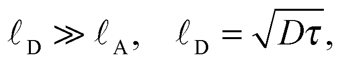
In order to attain a high efficiency, a semiconductor has to fulfill some basic requirements. In particular, an ideal solar cell requires: (i) a short absorption length (![[small script l]](https://www.rsc.org/images/entities/char_e146.gif) A); (ii) large recombination life-times τ for carriers; and (iii) high carrier mobilities μ. In total, the following condition should hold for the diffusion length
A); (ii) large recombination life-times τ for carriers; and (iii) high carrier mobilities μ. In total, the following condition should hold for the diffusion length
 | (1) |
Available data indicate that the diffusion length for perovskite semiconductors can vary from 1 up to 175 (μm).5–7 These lengths correspond to the carrier lifetimes from a few nanoseconds to a few hundreds microseconds. It has already been mentioned above that such a variation may be determined by material purity, i.e., by different densities of light trapping center assisted non-radiative recombination, i.e., the Shockley–Read–Hall (SRH) recombination (see details in ref. 8). Evidently, the power-conversion efficiency of perovskite solar cells could be increased when non-radiative recombination pathways are eliminated.9 Indeed, a stand-alone radiative recombination yields very large carrier lifetimes of the order of a few hours (see ref. 10, p. 301). The question arises: what degree of the purity could be enough to reach the Shockley–Queisser limit for perovskite solar cells? In this contribution we shall attempt to elucidate this question and determine the maximal efficiency that corresponds to this limit in perovskite solar cells.
2 Model
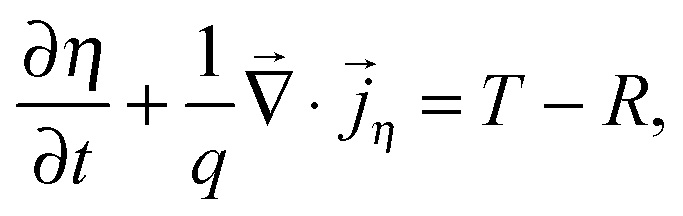
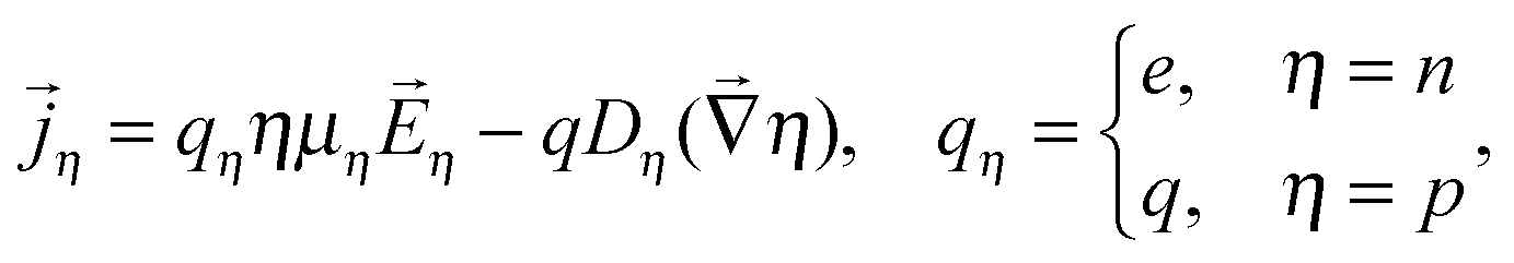
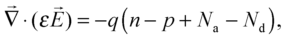
To analyse various effects in the PVE simulation that can exert an influence on the efficiency, we employ a phenomenological approach to carrier transport, proposed originally for two-valley semiconductors.11 It allows incorporation of transition rates for carrier transfers into the continuity equations for electrons in a conduction band and for holes in a valence band.We consider the following set of equations for electron/hole density η = n/p:
 | (2) |
 | (3) |
 | (4) |
![[j with combining right harpoon above (vector)]](https://www.rsc.org/images/entities/i_char_006a_20d1.gif) = n − p, = n − p, | (5) |
 | (6) |
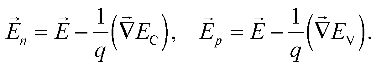
Here, T(R) is the photo- or impact ionization (the recombination) rate of carriers per unit volume, Na/Nd is the ionized acceptor/donor density, EC(EV) is the edge energy of the conduction (valence) band, and ε is the permittivity. Evidently, eqn (4) transforms to the Poisson's equation, since the electric field strength  is related to the scalar potential ϕ.
Note that the mobility and the diffusion coefficient depend on mean carrier energy εη. Therefore, to complete the scheme we extend the considered approach by adding the continuity equations for the energy density ![[scr E, script letter E]](https://www.rsc.org/images/entities/char_e140.gif) η = η·εη of electron–hole plasma
η = η·εη of electron–hole plasma
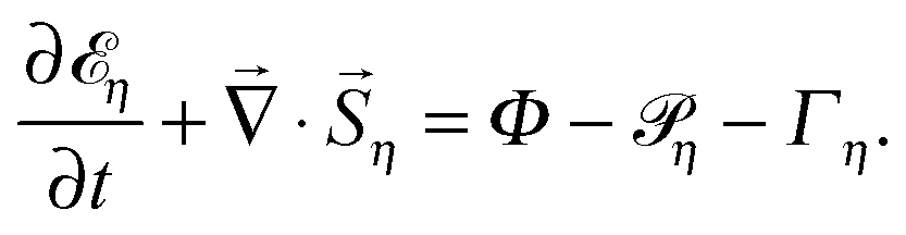 | (7) |
![[scr P, script letter P]](https://www.rsc.org/images/entities/char_e52f.gif) η = η·
η = η·![[E with combining right harpoon above (vector)]](https://www.rsc.org/images/entities/i_char_0045_20d1.gif) η; Γη = η(εη − ε0)/τεη, where τεη is the energy relaxation time, ε0 = 3kBT0/2. The energy flux density
η; Γη = η(εη − ε0)/τεη, where τεη is the energy relaxation time, ε0 = 3kBT0/2. The energy flux density ![[S with combining right harpoon above (vector)]](https://www.rsc.org/images/entities/i_char_0053_20d1.gif) η has the following form:
η has the following form: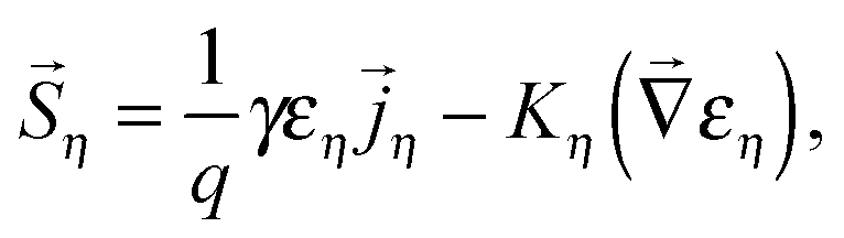 | (8) |
A few remarks are in order. In a low electric field we use constant mobility (low-field mobility). With the increase of the electric field the carrier velocity increases asymptotically towards a maximal value, i.e., the saturation velocity vsη. As is mentioned above, in our approach the carrier mobilities are functions of mean carrier energies and are determined by the following conditions:
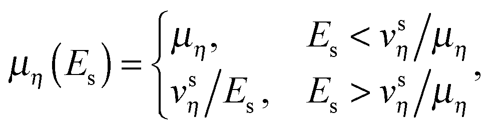 | (9) |
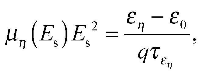 | (10) |
Standard drift-diffusion models either overestimate drift velocities in the case of constant carrier mobilities or underestimate them (see discussion in ref. 13) in the case of the field dependent mobilities such as (9). Note that the correct description of the drift velocities at early time dynamics is especially useful in the simulation of the transient current while modelling the real-time current–voltage measurements. In addition, this description is important for reliable calculations of capacitance frequency dispersion of the PVE, i.e., the frequency dependence of the permittivity for perovskite solar cells.
We have introduced in eqn (7) the photogenerated rate of the energy density of free carriers at the depth x from a semiconductor surface:
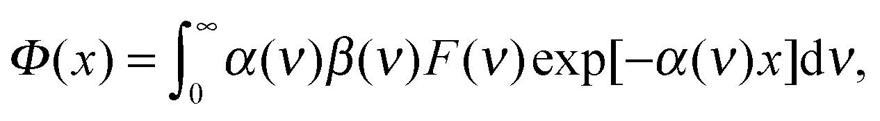 | (11) |
The photoionization rate T(x) is defined in a similar way
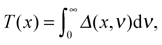 | (12) |
| Δ(x,ν) = α(ν)F(ν)exp[−α(ν)x], | (13) |
| R = (np − ni2)/(τpn + τnp). | (14) |
We consider a typical planar heterojunction architecture (see Fig. 1), where the following parameters are used. The minimal width of ZnO and CuI layers (≃0.2 μm) has been taken to ensure that it is large enough than the charged layers on the boundaries with perovskites. The parameters for the contacts and the perovskites for ZnO/CH3NH3PbI3/CuI (see ref. 14 and 15) are as follows: (a) the relative dielectric constant is 9/1000/6.25; the effective electron mass is 0.275/1/0.3 (×me); the effective hole mass is 0.59/1/2.4 (×me); the electron mobility is 150/50/50 (cm2 (V s)−1); the hole mobility is 50/50/44 (cm2 (V s)−1); all energy relaxation times are 10−12 (s); the carrier lifetime (τn = τp) is 10−9/τx/10−9 (s). In our analysis we vary τx from a few nanoseconds to a few hundreds of microseconds. Here, me is a free electron mass. We would like to mention one more point that deserves attention: the permittivity of perovskite solar cells may increase 1000 times under 1 sun illumination compared to dark conditions (see Fig. 2d in ref. 3 and the following discussion). In addition, we have also checked that the decrease of the permittivity (chosen in our calculations to be equal to 1000 for perovskite solar cells) on two orders of magnitude does not affect our results.
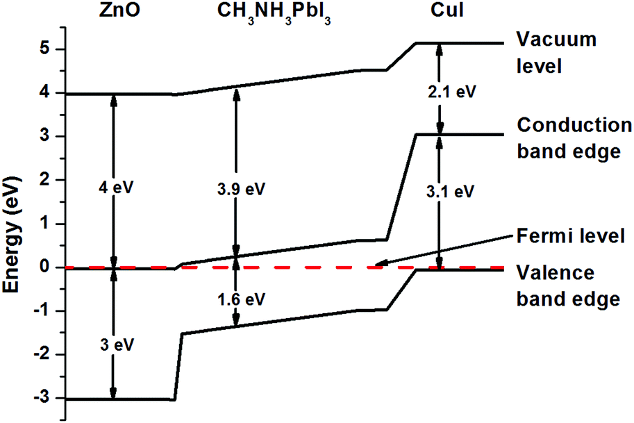 | ||
| Fig. 1 Band profile of the CH3NH3PbI3 p–i–n solar cell. The following data are taken from ref. 14 and 15 for ZnO, the perovskite, and CuI, respectively: (a) band gap energies are 3; 1.6; 3.1 (eV); (b) electron affinity EEA = 4; 3.9; 2.1 (eV). The built-in potential Vbi ≃ 1.17 V. The width of ZnO and CuI layers is 0.2 μm, while the width of CH3NH3PbI3 is varied, in order to find the optimal thickness of the perovskite structure (see Section 3). | ||
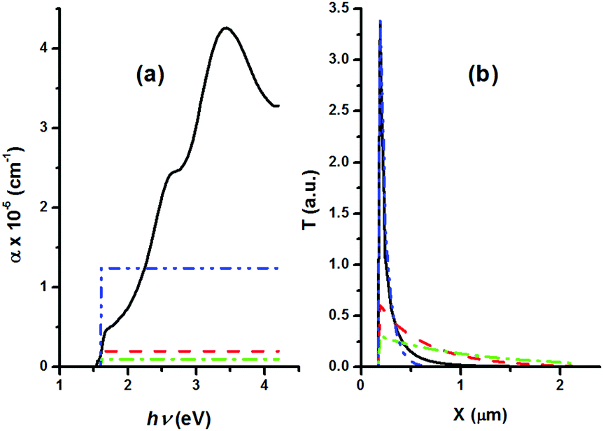 | ||
Fig. 2 (a) Absorption coefficient α as a function of the photon energy: (i) experimental values are connected by solid (black) line; (ii) auxiliary values = 10![[thin space (1/6-em)]](https://www.rsc.org/images/entities/char_2009.gif) 000, 20000, 124200 (cm−1) are displayed by dashed (red), dotted-dashed (green), dashed-dot-dot (blue) lines. (b) The photoionization rate (12) as a function of the depth x from the irradiated surface for various profiles of the absorption coefficient α. Note that the value (= 124200 cm−1) generates the photoionization rate that closely follows the experimental dependence. 000, 20000, 124200 (cm−1) are displayed by dashed (red), dotted-dashed (green), dashed-dot-dot (blue) lines. (b) The photoionization rate (12) as a function of the depth x from the irradiated surface for various profiles of the absorption coefficient α. Note that the value (= 124200 cm−1) generates the photoionization rate that closely follows the experimental dependence. | ||
To investigate the efficiency of the planar heterojunction architecture we have to solve the set of eqn (2)–(14) using the following boundary conditions. At the left boundary, in heavily doped ZnO the majority carrier concentration is set to the value n = Nd = 1019 (cm−3), while the minority one is set to the value p = ni2/Nd. Here, ni2 is a carrier concentration in the intrinsic semiconductor (see for details ref. 16). The opposite situation occurs over heavily doped CuI (the right boundary), where the majority carrier concentration is set to the value p = Na = 1019 (cm−3), while the minority one is set to the value n = ni2/Na. We assume that at the boundaries electron and hole subsystems have average energies εn = εp = 3kBT0/2, i.e., they are in thermal equilibrium.
3 Discussion of results
When the p–i–n system is illuminated, light creates electron–hole pairs in the perovskite layer, while the contact layers are considered to be transparent. For our analysis we use the experimental evolution of the absorption coefficient α as a function of the incident light energy,17 the Air Mass 1.5 Sun spectrum, and the lattice temperature T0 = 300 K. In our calculations it is assumed that: (i) the quantum efficiency = 1, and there is no reflection from the PVE. The maximum of the absorption is observed for very energetic photons ∼3.5 eV. Evidently, only photons with the energy hν − Egap > 0 are absorbed and generate electron–hole pairs. Fig. 2 demonstrates that the majority of photogenerated carriers are created in a narrow layer of thickness L ≤ 0.5 μm from the irradiated surface. The stepwise absorption coefficients illustrate as well the same tendency as the experimental absorption coefficient. Namely, the decrease of the coefficient increases effectively the absorption lengthA due to the increase of the photon penetration distance x from the irradiated surface of the p–i–n system. In fact, the increase of the absorption length leads to the increase of the optimum perovskite thickness. It is noteworthy that one can fit experimental absorption coefficient spectra by some step functions.
In order to define the current–voltage characteristics (CVC) of the considered system, one has to extract the contact potential difference from the applied voltage to the p–i–n structure by means of the standard procedure.16 At a given voltage applied to the solar cell under the incident light, we are able to define the current over contacts. The numerical approach to the solution of the set of equations is discussed in detail in ref. 18. The results of CVC calculations of the PVE are displayed in Fig. 3, while the PVE power conversion efficiency in Fig. 4.
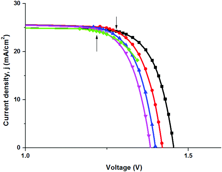 | ||
| Fig. 3 Current density as a function of applied voltage at the diffusion length D = 150 μm. Various perovskite film widths are considered: (a) solid (black) squares are used to connect the results for L = 0.5 μm; (b) solid (red) circles are used to connect the results for L = 1 μm; (c) solid (blue) up triangles are used to connect the results for L = 1.5 μm; (d) solid (pink) down triangles are used to connect the results for L = 2 μm; (f) solid (green) diamonds are used to connect the results for L = 0.5 μm with the series resistance R = 2.5 Ohm cm2. Arrows indicate the maximum efficiency for the PVE with L = 0.5 μm and L = 2 μm. | ||
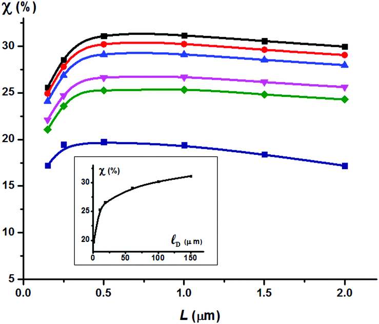 | ||
| Fig. 4 The efficiency of the p–i–n solar cell as a function of the perovskite film thickness for different diffusion lengths D. Various values for the diffusion length are considered: (a) solid (navy) squares are used to connect the results for D = 1 μm; (b) solid (green) diamonds are used to connect the results for D = 10 μm; (c) solid (pink) down triangles are used to connect the results for D = 18.7 μm; (d) solid (blue) up triangles are used to connect the results for D = 60 μm; (e) solid (red) circles are used to connect the results for D = 100 μm; (f) solid (black) squares are used to connect the results for D = 150 μm. The insert displays the efficiency of the p–i–n system as a function of the diffusion length D. All results are obtained with the aid of the experimental absorption coefficient α displayed in Fig. 2a. | ||
The maximal efficiency of the p–i–n system is developed at the perovskite film thickness L = 0.5 μm at the diffusion length D = 1 μm. The increase of the length values 10 < D < 150 μm leads to the shift of the maximal efficiency to the thickness ∼1 μm. A further increase of the thickness L decreases the efficiency of the p–i–n system. Below we provide a few arguments that allow us to shed light on this result.
In fact, the output voltage U of the considered system at the maximal efficiency could be approximated by a simple expression
U = ![[scr F, script letter F]](https://www.rsc.org/images/entities/char_e141.gif) − R·j, − R·j, | (15) |
is the system e.m.f. and R is the intrinsic resistance. Our calculations demonstrate that the results for L = 2 μm coincide with a good accuracy with those obtained for L = 0.5 μm plus the parasitic resistance R = 2.5 Ohm cm2. Note, however, that the estimation of the ohmic resistance (due to the thickness excess) yields a very small value ROhm ∼ 10−3 Ohm cm2. This estimation is obtained with the aid of the calculations of carrier concentrations (see Fig. 5) by means of the solution of the set of eqn (2)–(14). Thus, the parasitic resistance has a non-ohmic origin.
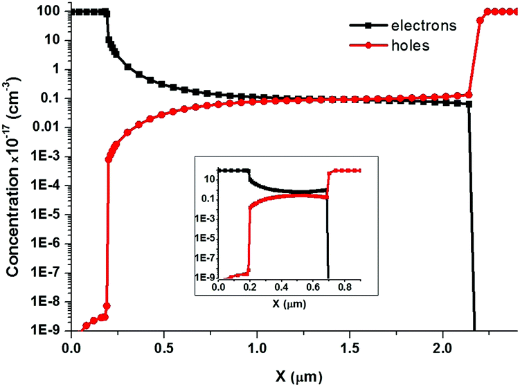 | ||
| Fig. 5 Carrier densities in the illuminated p–i–n system at the positive bias U = 1.25 V and the diffusion length D = 150 μm. The variable x characterises the distance from the irradiated surface in the perovskite absorption film with the thickness L = 2 μm. The insert displays similar results for the thickness L = 0.5 μm and U = 1.29 V. Both PVEs are biased to obtain a maximum efficiency. | ||
To gain a better insight into the nature of this resistance let us focus on the flux of energy density, dissipated by electron and hole currents in the semiconductor lattice, and defined formally by the last term Γ in eqn (7). Once the steady solutions for electron/hole densities are obtained, one can calculate this term. Fig. 6 displays the dissipated power density at the CVC point that corresponds to the maximum efficiency of the p–i–n solar cell (as an example of the CVC, see Fig. 3 at the diffusion length D = 150 μm). Evidently, the amount of dissipated energy increases with the increase of the thickness of the perovskite film for all diffusion lengths. We observe, however, that at the diffusion length D = 1 μm the dissipation reaches the maximal value at the thickness L = 1.5 μm. A further increase of the thickness above this value yields a slight decrease of dissipation. In this case the thickness exceeds the diffusion length, and, consequently, the current decreases due to the SRH recombination, which decreases the dissipation. The efficiency of such PVEs is much lower, and decreases much faster in comparison with those with D > 1 μm (see Fig. 4).
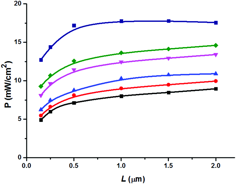 | ||
| Fig. 6 Power density dissipated by electron and hole currents in the semiconductor lattice at the maximum efficiency of the p–i–n solar cell as a function of the perovskite film thickness for different diffusion lengths D. Various values for the diffusion length are considered: (a) solid (navy) squares are used to connect the results for D = 1 μm; (b) solid (green) diamonds are used to connect the results for D = 10 μm; (c) solid (pink) down triangles are used to connect the results for D = 18.7 μm; (d) solid (blue) up triangles are used to connect the results for D = 60 μm; (e) solid (red) circles are used to connect the results for D = 100 μm; (f) solid (black) squares are used to connect the results for D = 150 μm. | ||
One can readily evaluate the parasitic resistance from the dissipated power density
| P = j2 × R. | (16) |
At the maximal efficiency point, for the PVE with the diffusion length D = 150 μm one obtains the resistance R0.5,2 = 12.3(14.8) Ohm cm2 for the thickness L = 0.5(2) μm, respectively. As a result, the parasitic resistance is R = R2 − R0.5 = 2.5 Ohm cm2. Thus, the non-ohmic origin of the parasitic resistance is determined by the dissipated energy of the carriers.
The distribution profile of the dissipation is extremely nonhomogenous along the sample thickness (see Fig. 7). This explains the non-ohmic character of the parasitic resistance. For the sake of illustration, we choose the profile of the dissipation for a particular thickness L = 2 μm at the diffusion length D = 150 μm. The main contributions to the dissipation are brought about by the junction regions. There is a transfer of the carrier energy into the lattice of ZnO, which generates heat (P > 0) in the junction, and the absorption of the energy (P < 0) by the carriers from the perovskite lattice. The latter process is replaced by a slight heating of the perovskite lattice, at some distance away from the junctions, and transforms to a slight cooling in the neighborhood of the right junction. Immediately, after the junction area perovskite-CuI, the heat is generated noticeably by the carriers. In the considered planar heterojunction architecture this phenomenon resembles closely the Peltier effect.
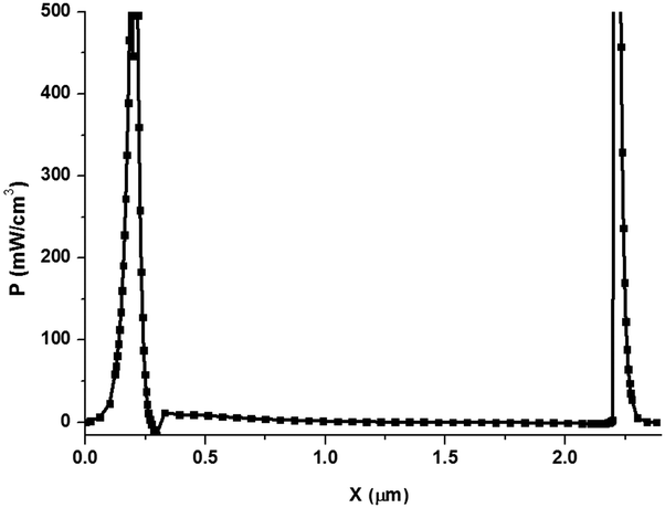 | ||
| Fig. 7 Power density dissipated by electron and hole currents in the semiconductor lattice at the maximum efficiency of the p–i–n solar cell as a function of the distance from the irradiated surface. The cell thickness is L = 2 μm, and the diffusion length is D = 150 μm. | ||
Thus, varying the diffusion length D in the perovskite absorber and its thickness, we have determined the efficiency of the p–i–n system (see Fig. 4). Evidently, the larger the diffusion length, the better the efficiency. However, two features are found. First, all the efficiency curves change the slope once the average thickness approaches the value L ≃ 1 μm, except the case D = 1 μm where the optimal thickness is L = 0.5 μm. The further increase of the perovskite thickness yields the parasitic resistance. As a result, the efficiency drops down for all values of the diffusion length. Second, the increase of the diffusion length above D = 150 μm does not increase essentially the efficiency of the p–i–n system. Note that this efficiency is approaching the value of 31%.
Unfortunately, there are no available data for our system. For the sake of illustration of the efficiency of our approach, we compare the results obtained within our model and available experimental data for the system with a similar planar heterojunction architecture studied in ref. 1. Starting from the thickness L = 0.5 μm of this system, we vary the following parameters: the reflection coefficient, the carrier lifetimes, and the parasitic resistance connected in series with the PVE, in order to reproduce the experimental CVC.1 In our calculations we use the experimental behaviour (data) of the absorption coefficient [see Fig. 2(a)]. The reflection coefficient (= 0.18) is determined from the equivalence of the model and experimental values of the short-circuit current. The calculations of the carrier lifetime (obtained from the condition of equivalence of the model and experimental values of the open circuit voltage) yields the value = 0.84 ns that corresponds to the diffusion length D = 0.33 μm. The parasitic resistance (= 6.5 Ohm cm2) is determined from the equivalence of the model and experimental values of the fill factor. The obtained values enable us to reproduce the experimental CVC with a remarkable accuracy (see Fig. 8).
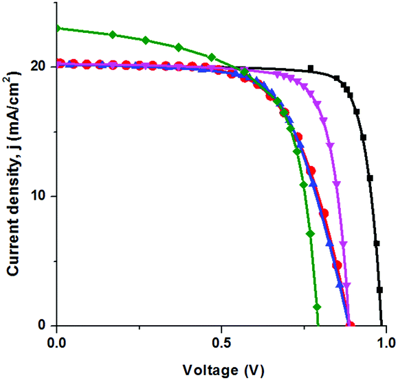 | ||
| Fig. 8 Current density as a function of applied voltage: (a) solid (red) circles are used to connect the experimental results;1 (b) solid (green) diamonds are used to connect the model results for D = 0.12 μm with zero reflection coefficient; (c) solid (black) squares are used to connect the results for D = 1 μm and the reflection coefficient is 0.18; (d) solid (pink) down triangles are used to connect the results for D = 0.33 μm and the reflection coefficient is 0.18; (e) solid (blue) up triangles are used to connect the results for D = 0.33 μm, the reflection coefficient is 0.18 with the series resistance R = 6.5 Ohm cm2. | ||
Finally, based on our results, let us provide a simple estimation of the energy associated with hot electrons/holes. The incident light, characterised by the Air Mass 1.5 Sun spectrum, carries the power of 100 mW cm−2. Our solar cell with the absorption coefficient (see Fig. 2a) and the thickness L = 2 μm absorbs in one unit of time 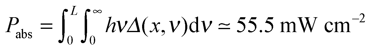 . The efficiency of the solar cell (see Fig. 4) yields the useful power Puse ≈ 30 mW cm−2. We have to take into account the dissipated energy which is
 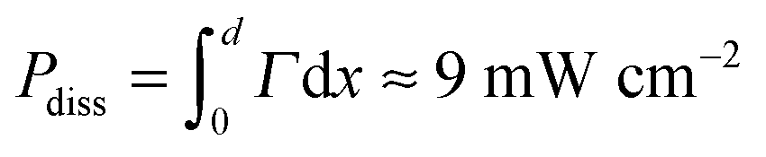 (see Fig. 6), where d is the length of the heterostructure. Some energy is carried out due to the SRH recombination. It is natural to assume that the minimal lost energy is defined by the energy gap. Knowing the solution of eqn (2)–(14), one can evaluate this lost energy as
 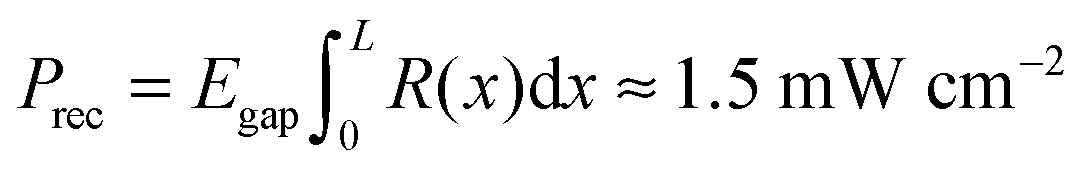 . From these estimations we can readily determine the power that heats the electron/hole plasma
| Phot = Pabs − Puse − Pdiss − Prec, | (17) |
4 Conclusions
We would like to mention that in contrast to a large variety of drift models for evaluation of solar cell perfomance, we developed an approach that starts from basic semiconductor physics and builds up a transport model with kinetic coefficients that are functions of carrier energy densities. It is akin in spirit to the approach developed in ref. 19. We treat, however, electron and hole collecting materials explicitly but not with the aid of boundary conditions, as it is done in ref. 19. This allows us to trace, for example, the influence of permittivities of the basic elements of the p–i–n junction solar cell on the power conversion efficiency. In addition, as far as we know, the inclusion of the continuity equations for the energy density of electron–hole plasma (see eqn (7) and (8)) in a general scheme is their first time application in the physics of solar cells. These equations allow establishing a detailed balance between an incident sun power and its dissipation inside the PVE and in the load.We have numerically solved transport equations for the carrier and energy densities in the p–i–n system. The obtained results allow us to shed light on dissipation processes in the considered PVE and to trace the evolution of the energy gained by electrons and holes from the sunlight excitation. By varying the diffusion length, we found that there is an optimal thickness of the perovskite absorber L ≃ 1 μm. Once the purity of the perovskite absorber allows reaching the diffusion length D ≤ 150 μm, the considered system is able to attain the efficiency ∼31% in the Air Mass 1.5 spectrum.
Acknowledgements
This work was supported in part by Russian Science Foundation, grant no. 15-13-00170.References
- G. E. Eperon, V. M. Burlakov, P. Docampo, A. Goriely and H. J. Snaith, Adv. Funct. Mater., 2014, 24, 151–157 CrossRef CAS.
- N. G. Park, Mater. Today, 2015, 18, 65–72 CrossRef CAS.
- B. Chen, M. Yang, S. Priya and K. Zhu, J. Phys. Chem. Lett., 2016, 7, 905–917 CrossRef CAS PubMed.
- W. Shockley and H. J. Queisser, J. Appl. Phys., 1961, 32, 510–519 CrossRef CAS.
- C. Wehrenfennig, G. E. Eperon, M. B. Johnston, H. J. Snaith and L. M. Herz, Adv. Mater., 2014, 26, 1584–1589 CrossRef CAS PubMed.
- S. D. Stranks, G. E. Eperon, G. Grancini, C. Menelaou, M. J. P. Alcocer, T. Leijtens, L. M. H. A. Petrozza and H. J. Snaith, Science, 2013, 342, 341–344 CrossRef CAS PubMed.
- G. C. Xing, N. Mathews, S. Y. Sun, S. S. Lim, Y. M. Lam, M. Grätzel, S. Mhaisalkar and T. C. Sum, Science, 2013, 342, 344–347 CrossRef CAS PubMed.
- J. Nelson, The Physics of Solar Cells, Imperial College Press, London, 2003 Search PubMed.
- G.-J. A. H. Wetzelaer, M. Scheepers, A. M. Sempere, C. Momblana, J. Ávila and H. J. Bolink, Adv. Mater., 2015, 27, 1837–1841 CrossRef CAS PubMed.
- S. G. Kalashnikov and V. L. Bonch-Bruevich, The Physics of Semiconductors, Main Editorial Board for Physical and Mathematical Literature, Moscow, Russian edn, 1990 Search PubMed.
- K. Blotekjaer, IEEE Trans. Electron Devices, 1970, ED–17, 38–47 CrossRef.
- Y. Apanovich, E. Lyumkis, B. Polsky, A. Shur and P. Blakey, IEEE Trans. Comp. Aided Design of Integrated Circuits, 1994, 13, 702–711 CrossRef.
- J. Ruch, IEEE Trans. Electron Devices, 1972, ED–19, 652–654 CrossRef.
- O. Madelung, Semiconductors: Data Handbook, Springer-Verlag, Berlin, 3rd edn, 2004 Search PubMed.
- M. A. Green, A. Ho-Baillie and H. J. Snaith, Nat. Photonics, 2014, 8, 506–514 CrossRef CAS.
- S. M. Sze and K. K. Ng, Physics of Semiconductors Devices, John Wiley & Sons, Inc., New Jersey, 3rd edn, 2007 Search PubMed.
- S. Sun, T. Salim, N. Mathews, M. Duchamp, C. Boothroyd, G. Xing, T. C. Sum and Y. M. Lam, Energy Environ. Sci., 2014, 7, 399–407 CAS.
- Y. B. Martynov, Comput. Methods Math. Phys., 1999, 39, 292–297 Search PubMed.
- Y. Zhou and A. Gray-Weale, Phys. Chem. Chem. Phys., 2016, 18, 4476–4486 RSC.
| This journal is © the Owner Societies 2017 |