
 Open Access Article
 This Open Access Article is licensed under a
 Creative Commons Attribution 3.0 Unported Licence
Charge transfer quantification in a SnOx/CuPc semiconductor heterostructure: investigation of buried interface energy structure by photoelectron spectroscopies
Maciej
Krzywiecki
 *ab,
Lucyna
Grządziel
b,
Adnan
Sarfraz
a and
Andreas
Erbe
ac
*ab,
Lucyna
Grządziel
b,
Adnan
Sarfraz
a and
Andreas
Erbe
ac
aMax-Planck-Institut für Eisenforschung GmbH, Max-Planck-Str. 1, 40237 Düsseldorf, Germany. E-mail: Maciej.Krzywiecki@polsl.pl; Fax: +48 32 237 22 16; Tel: +48 32 237 20 01
bInstitute of Physics – Center for Science and Education, Silesian University of Technology, S. Konarskiego Str. 22B, 44-100 Gliwice, Poland
cDepartment of Materials Science and Engineering, NTNU, Norwegian University of Science and Technology, Trondheim, Norway
First published on 26th April 2017
Abstract
A tin oxide/copper phthalocyanine (CuPc) layer stack was investigated with two complementary photoemission methods. Non-destructive analysis of the electronic properties at the SnOx/CuPc interface was performed applying angle-dependent measurements with X-ray photoelectron spectroscopy (ADXPS) and energy-resolved photoemission yield spectroscopy (PYS). The different components (related to oxide layer and organic overlayer as well as to contamination features) observed in the spectra were assigned to a particular layer by relative depth plot analysis. ADXPS allowed determination of the chemical and electronic structure of the investigated samples. The addition of the organic ultra-thin film to the oxide layer caused a significant increase of the structure's photoemission yield. The combination of ADXPS and PYS allowed determination of the work function of constituent layers, and charge transfer phenomena at the SnOx/CuPc buried interface. An interface dipole of 0.23 eV was detected, assigned to charge transfer across the interface from the oxide layer towards the organic film. The energy level alignment at the SnOx/CuPc interface was determined, and presented in a band-like diagram, together with depth-dependent changes of the core energy levels of the structure's constituents. Finally the role of the oxide's defect-related energy levels in the charge transfer was discussed. The results obtained exhibit significance ranging from investigation, basic understanding and application of such hybrid films. Application of these results in hybrid electronic devices can help understanding and furthering this technology.
Introduction
In recent times, low-dimensional nanoscale materials have attracted more and more attention owing to a number of technological applications.1–3 Among them hybrid materials and the creation of inorganic–organic heterojunctions are especially under rapid development owing to their vast range of applications, ranging from photovoltaics4,5 through other optoelectronic and thermoelectronic devices6–8 to inorganic–organic transistors.9 Although a number of systems and their characterization have been presented recently in the field of hybrid materials,10,11 there is a significant need to search for cost-effective technologies, including cheap and non-precious materials, and characterization methods.Among inorganic materials for heterojunctions, tin oxides are interesting semiconducting materials that promise a wide variety of technological applications, such as energy conservation or photovoltaic devices.12 Tin oxides are a group of wide band gap transparent oxides in which the deviation from stoichiometry as well as the presence of additional defects and impurities creates states in the band gap, modifying its electronic structure. A targeted modification can hence be used to tune to a desired application.13
Good candidates for the organic part of the junction are metallophthalocyanines (MePc), molecular semiconductors with high chemical stability and good electrical and optical properties.14 An excellent representative MePc is copper phthalocyanine (CuPc), which up to the last decade was used mainly as a dye. CuPc is now becoming a more and more popular organometallic compound that is already applied in third generation solar cells, gas sensors and advanced opto-electronic technologies.15–17
Inorganic–organic junctions based on tin oxides have been investigated recently,18–20 however the focus was on characterization and modification of the tin dioxide as the inorganic part of the junction. Works focusing on the properties of the interface between SnOx and the organic material are still rare.21
The origin of device efficiency is often related to the inorganic–organic junction properties, and to the physical phenomena occurring at the buried heterojunction.22,23 It is especially important in the case of ultra-thin layers where the Debye screening length is in the order of the layer thickness, as the surface, subsurface and interfacial phenomena can affect the quality and efficiency of component operation.24 Therefore, monitoring the processes at the interface, including charge carrier transfer together with interfacial electronic and chemical properties and energy level alignment, becomes crucial for optimal performance of heterostructures.
Several approaches have been used for comprehensive investigation of the buried interfaces, e.g. (i) step-by-step deposition and simultaneous investigation,25 (ii) ion-etching-assisted examinations,26 and (iii) synchrotron radiation-based photoelectron spectroscopy experiments.27 Though these methods yield detailed information, they possess a number of disadvantages, like complicated setup combining processing technology with detection (i and iii), possible sample damage with the probability of selective etching (ii), and finally, the overall cost limits general accessibility.
Therefore, in the case of ultra-thin layered systems, angle-dependent photoemission measurements are at the center of attention, as these permit non-destructive examination of layered samples with extremely low influence of the probing medium onto the structure being probed. Another advantage is the ability to use standard lab-based experimental techniques for post-process quality assessment of the structures.
The methodology was described in our previous study28 on ultra-thin tin oxide nonstoichiometric layers examined with Angle Dependent Photoelectron Spectroscopy (ADXPS). This work represents one step forward: to the prepared tin oxide layer, we are adding an ultra-thin CuPc layer that results in a hybrid heterojunction at the buried interface between SnOx (x ≈ 1.25) and CuPc. Owing to the perspective application of this SnOx/CuPc system in hybrid electronics, it should be possible to fully recognize the creation of the interface between the layers. In order to augment the ADXPS with the ability to determine the electronic properties (e.g. work function) at the interface, photoemission yield spectroscopy (PYS) was applied. Owing to the similar probing depth as in XPS, this method is well-suited for complementing investigations of the buried interfaces.
This work describes the fabrication of a thin film inorganic/organic hybrid junction based on SnOx, and the detailed characterization of its electronic structure and chemical composition. Particularly, there are two main objectives of the presented work. The first is to demonstrate the ability of the combination of ADXPS and PYS spectroscopies for investigation of electronic phenomena at inorganic/organic buried interfaces. The second is to apply this methodology for the evaluation of energy level alignment at the hybrid SnOx/CuPc nanostructure.
Experimental details
The SnOx/CuPc samples were prepared on silicon Si(100) wafer substrates (SiMat, n-type, P-doped, 5–10 Ω cm). Silicon wafers were first cleaned in an ultrasonic bath in acetone, isopropanol, and de-ionized water sequentially for 15 min per each cleaning medium. Then, the substrates were blown with nitrogen and dried in a furnace at 110 °C for 30 min.SnOx sol (0.025 M) was prepared by mixing tin(IV) isopropoxide with triethylamine (TEA) in a molar ratio of 1![[thin space (1/6-em)]](https://www.rsc.org/images/entities/char_2009.gif) :2, and subsequent dilution with isopropanol. All reagents were used as purchased from VWR International. Prior to sol deposition, the substrates were functionalized by rinsing with 0.007 M TEA in isopropanol and then immediately dried with nitrogen. The spin-coating process (Spin-coater P6700, Specialty Coating Systems Inc.) was conducted at 500 rpm for 2 s, 2000 rpm for 8 s and 6000 rpm for 20 s. Immediately after deposition, the samples were dried in air for 10 min at 110 °C. Finally, samples were annealed in a tube furnace at 550 °C for 4 h in ambient atmosphere.
:2, and subsequent dilution with isopropanol. All reagents were used as purchased from VWR International. Prior to sol deposition, the substrates were functionalized by rinsing with 0.007 M TEA in isopropanol and then immediately dried with nitrogen. The spin-coating process (Spin-coater P6700, Specialty Coating Systems Inc.) was conducted at 500 rpm for 2 s, 2000 rpm for 8 s and 6000 rpm for 20 s. Immediately after deposition, the samples were dried in air for 10 min at 110 °C. Finally, samples were annealed in a tube furnace at 550 °C for 4 h in ambient atmosphere.
The CuPc ultra-thin layers were deposited in an ultra-high vacuum system by PVD. The system base pressure was lower than 5 × 10⁻⁷ Pa. Prior the deposition, the CuPc powder was degassed and purified by heating the crucible up to 240 °C for 5 h. The evaporation process was controlled by quartz crystal microbalance (PREVAC TMC-13). In order to obtain uniform CuPc films, the evaporation rate was kept at the level of 0.1 Å s−1.
ADXPS was carried out on a Physical Electronics PHI Quantera II spectrometer equipped with an Al Kα micro-focused source (spot diameter <100 μm) and a dual-beam charge neutralizer. The survey spectra were recorded with an energy step of 0.4 eV and the pass energy set to 140 eV. The individual core level spectra were recorded with an energy step 0.025 eV and the pass energy set to 26 eV. The XPS system base pressure was 2 × 10⁻⁸ Pa. All XPS spectra were recorded with varying take-off angles (TOA, defined as the angle between the analyzer axis and sample's plane normal) from 0° to 70°. The acceptance angle of the analyzer was set to ±4°.
XPS data were analyzed by curve fitting using CASA XPS software.29 Each peak was represented by Gaussian (70%) and Lorentzian (30%) lines. The secondary electron background was subtracted with use of the Shirley function. The full width at half maximum (FWHM) of the components at the same energy region was allowed to vary within a narrow range. We used the lowest possible number of components to obtain acceptably low residual values. The estimated uncertainty for a particular component energy position was 0.04 eV. Quantitative analysis, including component ratio determination, was done with use of CASA XPS embedded relative sensitivity factors (RSF) and algorithms. The binding energy (B.E.) scale was calibrated to Au 4f7/2 (84.0 eV)30 recorded for the gold plate placed in the same sample holder.
For the information depth estimation, the same procedure as in our previous study was applied.28 The procedure is based on the algorithm introduced by Opila and Eng,31 which is also utilized by major equipment providers.32 Assuming that the intensity I of the photoelectron signal is a function of information depth d, it can be approximated as:31I = I0exp(−d/λcosΘ), where I0 is the intensity at the bare surface, λ is the electron escape depth and θ is the TOA. In the current work an information depth of 0 nm is assigned to the vicinity of SnOx/CuPc interface.
It has to be stated that the depth estimation was performed with the following assumptions: (i) ∼65% of the photoelectron signal comes from a depth of less than electron attenuation length λa (with this assumption λa = λ),33 (ii) diffraction and scattering of the photoelectrons is negligible, (iii) the layer is continuous, (iv) the X-ray intensity is essentially unattenuated throughout the analyzed layer and (v) λa is constant within the examined film.
All of the necessary values of λa were calculated with the use of the NIST electron inelastic mean free path database and electron attenuation length software.34 The embedded algorithms are based on analysis proposed by Werner35 using the TPP-2M (Tanuma–Powell–Penn)36 algorithm. The λa for the substrate Sn 3d peak in the CuPc organic overlayer was determined to be 2.54(5) nm. Following the analysis procedure that was used for SnOx characterization28 and was originally proposed by Cumpson,37 the total thickness of the CuPc layer was determined as 2.75(25) nm, which agreed with the indications of the QCM (3.00 nm).
PYS measurements were also done under UHV conditions (system base pressure 7.5 × 10⁻⁸ Pa). The samples were irradiated with UV light from a deuterium source, which was passed through a Zeiss™ monochromator providing the excitation range 200–400 nm (3.1–6.2 eV) with a resolution of 1 nm. The spectral intensity of light was monitored by a Rohre M12FQC51 photomultiplier. The sample was irradiated utilizing a fiber-based optical path with calibrated photon spectral intensity of the incident photon flux, assuring the independency of the photoemission yield from any external conditions. The photoemission yield spectra were recorded using a spectrometer utilizing a Hamamatsu channeltron electron multiplier and a SemiInstruments™ acquisition setup.
All of the uncertainties were estimated based on the standard uncertainty propagation methods, which can be found elsewhere.38 The uncertainty analysis takes into account possible charging effects39,40 angular broadening41 and random errors that could occur during the experiment.
Results and discussion
The chemical composition of the obtained bi-layer system was checked initially on the basis of the Sn 3d and O 1s XPS energy regions. Fig. 1 presents a decomposition of the O 1s energy region. The two evident components have been assigned to oxygen bonded to tin (lower binding energy) and to adsorbed oxygen contamination (higher binding energy). The latter might originate from oxygen uptake from the environment, water vapor or carbonaceous species. The oxygen uptake was already observed in the literature and in our former studies.42 The inset to Fig. 1 presents the Sn 3d energy region. | ||
| Fig. 1 O 1s and Sn 3d (inset) main substrate core energy levels recorded at TOA = 90° for SnOx/CuPc samples. The contributions from two components, identified as O–Sn bonding and contaminating oxygen (Ocont), are well visible. The purple line represents Shirley-type background. | ||
The peaks show high symmetry. Comparing these results to our previous studies28 leads us to conclude that no additional components appeared in the O 1s and Sn 3d energy regions, which suggests a lack of any covalent bonding created between the substrate oxide layer and the organic overlayer.
To support this statement and to investigate the chemical composition of the CuPc layer after deposition, the most representative C 1s, N 1s and Cu 2p energy regions were analyzed. The C 1s decomposition agrees with the standard for CuPc components, i.e. C–C and C–N together with their satellites and expected intensity ratios.43 The analysis of residual signal showed minor contamination of the layer with oxygen (as represented by the overlapping C–O/C![[double bond, length as m-dash]](https://www.rsc.org/images/entities/char_e001.gif) O component).44 This is in agreement with the O 1s region analysis made before. The Cu 2p region also exhibited a classical CuPc shape, with the very characteristic satellite feature (upper inset to Fig. 2). The last element to discuss in terms of the organic layer quality is the N 1s region (presented in the lower inset to Fig. 2). It also presents the one-component trace of the signal with a small satellite peak at the high binding energy side.43 Summarizing, there is no evidence in any signal, neither from the SnOx nor the CuPc side, of any covalent bonding between the SnOx substrate layer and the CuPc organic overlayer.
O component).44 This is in agreement with the O 1s region analysis made before. The Cu 2p region also exhibited a classical CuPc shape, with the very characteristic satellite feature (upper inset to Fig. 2). The last element to discuss in terms of the organic layer quality is the N 1s region (presented in the lower inset to Fig. 2). It also presents the one-component trace of the signal with a small satellite peak at the high binding energy side.43 Summarizing, there is no evidence in any signal, neither from the SnOx nor the CuPc side, of any covalent bonding between the SnOx substrate layer and the CuPc organic overlayer.
 | ||
| Fig. 2 Most characteristics for CuPc XPS energy regions: C 1s (main panel); Cu 2p with marked satellite feature (upper inset) and N 1s (lower inset). All presented regions were recorded at TOA = 90°. The purple line stands for Shirley-type background. | ||
As an introduction to electronic structure analysis, the investigation of the valance band (VB) – Sn 4d energy region is presented in Fig. 3 for TOA = 90°. The decomposition of the VB region (inset to Fig. 3) revealed the existence of the SnOx and CuPc components as expected. In general, for the SnOx layer the VB region should originate from mixing of the O 2p and Sn 5p/5s orbitals.45,46 The shape of the tin oxide-related peaks in this region shows strong similarities with the VB region of tin(IV) oxide, SnO2−δ.47 The SnOx investigated in this work is hence an oxygen-deficient tin(IV) oxide, in line with expectations, because a tin(IV)-based precursor was used. Based on our previous results28 the decomposition revealed the existence of the defect level states at the low binding energy side of the VB onset. Defect levels mainly originate from oxygen and tin vacancies; VO and VSn, respectively.48 The defect levels, hereafter referred to as VD, are the dominant signals in this energy region (i.e. close to the Fermi level49), and their analysis is done under the assumption that the contribution from the organic layer is suppressed by the oxide signal; this assumption will be discussed further within this manuscript. The organic layer contribution is represented by the existence of C 2p and N 2p components.
 | ||
| Fig. 3 VB—Sn 4d energy region recorded for TOA = 90°. The inset provides the magnification of the valance band region. The components originating from both the SnOx substrate and the organic overlayer are visible. The first component at the low-binding energy side originates from SnOx-related defect levels (VD). The purple line stands for a Shirley-type background. | ||
The assignment of the components is done on the basis of the available literature and databases,50 leaving open the possibility of misinterpretation, e.g. due to transport of impurities across the interface. In order to arrive at an unambiguous placement of the particular components, i.e. assign the components to the oxide or organic layer, a Relative Depth Plot (RDP) was applied.51 The RDP is a simple approach intended to point out the positioning of elements (or chemical states, if identified) in multilayered structures with respect to their surface or to the bulk. It does not provide absolute depth measurements and thickness, but indicates the location of the species on the relative depth plot connected to its average depth.52 The RDP is constructed for each species by calculating the natural logarithm of the ratio of the XPS peak area at near to the grazing emission angle to that at near to the normal emission.53 In general, species with higher relative depth are located closer to the surface, while those with lower depth are deeper into the bulk, thus determining the layer ordering.52
The RDP for the main SnOx- and CuPc-related components is presented in Fig. 4. Most of the components are placed as expected, i.e. C–C, N and C 2p components are originating from the organic overlayer. The components related to the oxide layer are, according to the RDP results: Sn–O, O–Sn, defect levels and carbon contamination. The VB SnOx component reflects the Sn 5p/5s peak position. An important result of this analysis is the confirmation that C 2p is a constituent of the CuPc signal, and the assignment of the VB SnOx and defect levels as originated from SnOx. It confirms the assignment of the components within the VB energy region made on the basis of chemical expectations (Fig. 3).
 | ||
Fig. 4 Scheme of the in-depth component placement analysis. The Y-axis scale shows the relative depth position scale of the component. Note that relative depth is not the same as the information depth used below. The cyan ( ) area stands for the CuPc layer and the gray ( ) area stands for the CuPc layer and the gray ( ) area for the SnOx layer. The white stripe in between represents the SnOx/CuPc interface. ) area for the SnOx layer. The white stripe in between represents the SnOx/CuPc interface. | ||
One more issue to be discussed from the RDP analysis is the contaminants' positioning in the SnOx/CuPc structure. The carbon contamination was located within the SnOx layer, which is consistent with findings made in ref. 28. It means that either the carbon contamination is solely originating from the SnOx layer, or the minor carbon contamination from the CuPc layer is being suppressed by the majority signal outgoing from the oxide layer. Next, the oxygen contamination was found to be placed at the interface between the organic and the oxide layer. This is highly probable since the oxygen-containing species from the environment would diffuse through the porous organic overlayer. However, this signal can also originate from oxygen species adsorbed at the SnOx surface before organic layer deposition. It is well known that Sn(IV) is a strong oxidant,54 so that in the presence of an electron donor, e.g. oxygen, it would lead to preferential oxidation of organics exactly at the interface.
The application of ADXPS and procedures described in ref. 28 allowed plotting the binding energy changes of the particular components as a function of the information depth for the organic overlayer. The components' energy change plots are depicted in Fig. 5. Because the method is based on the depth positioning with respect to the samples' surface and because all calculations (IMFP, attenuation length and others) take into consideration the CuPc-related material constants, the respective energy changes in the oxide layer have to be plotted a as function of TOA. In these terms, the higher the TOA, the more buried the majority signal measurement point is.
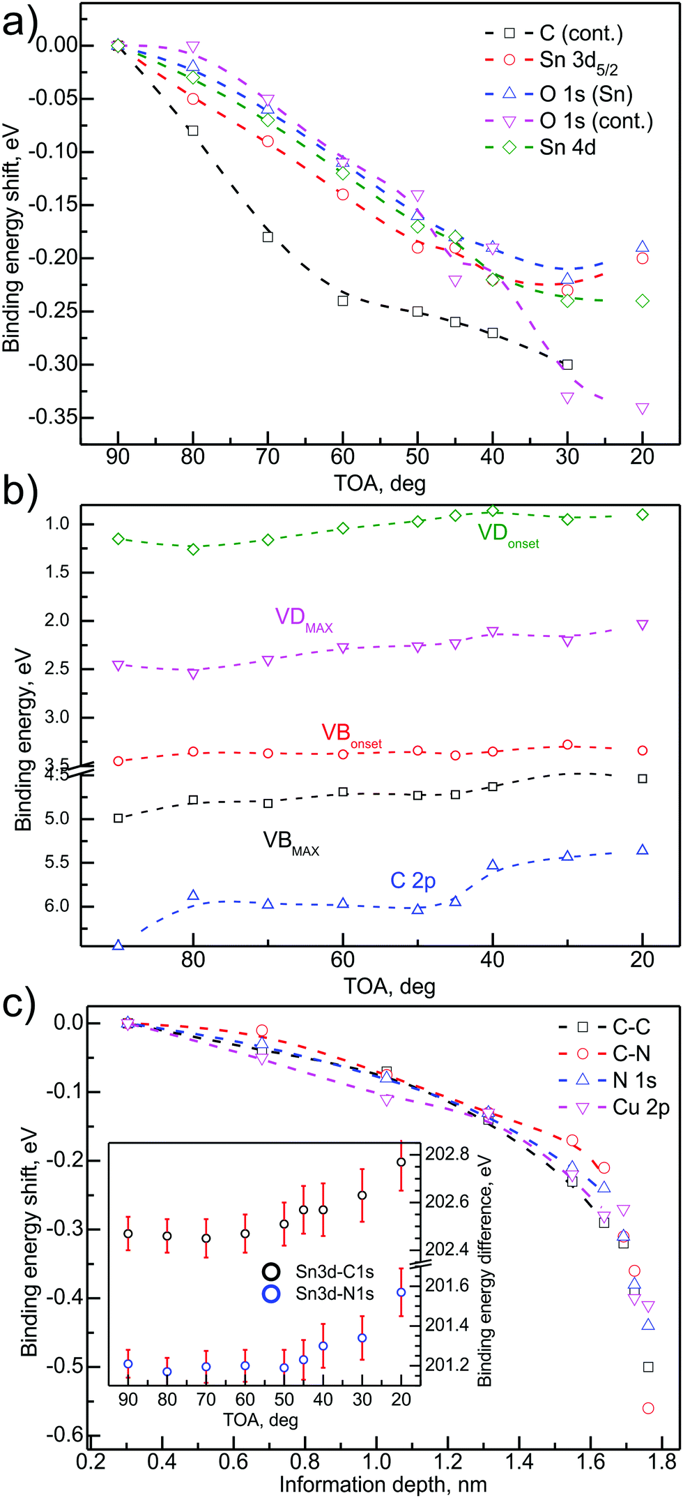 | ||
| Fig. 5 (a) Binding energy shift as a function of TOA for main SnOx-related core levels. (b) Variation of the binding energy of the VB-related energy levels as a function of TOA; (c) CuPc-related energy level shift as a function of information depth. Inset: Binding energy distance change as a function of TOA for the main SnOx- and CuPc-related core levels. Shift equal to 0 corresponds to no change from the initial value. | ||
Fig. 5(a) presents relative binding energy changes of the SnOx-related deep core levels, i.e. Sn 3d/4d and O 1s as a function of TOA. The plot contains also trace of carbon and oxygen contamination peaks. The evident shift of the levels can be observed with the magnitude varying from 0.20 eV to 0.35 eV, dependent on the component. It has to be kept in mind that the overall level shift is the sum of the chemical shift, changes in local electrostatic potential and possible charging effects.55 However, the shape of the changes trace for particular components rather excludes charging as the reason for the energy level shift—charging would imply the same shift for all of the components. Therefore, the conclusion drawn out from these data is that the major contribution to the energy change is the sum of the chemical shift and the changes in the electrostatic potential. The latter may arise from charge rearrangement at the SnOx/CuPc interface. Charge rearrangement at the interface will be further elaborated within the following paragraphs.
Fig. 5(b) presents the shift of the components that are most significant for the electronic structure of the valence band. For deeper analysis, the VBmax and VBonset are analyzed separately. The same procedure was applied to VD defect levels, which was analysed to yield VDmax and VDonset, respectively. Although the C 2p is a CuPc-related component and could be presented on a depth-dependent scale, it belongs to the VB region of the photoemission spectrum so in our opinion it is more appropriate to present it with the rest of the VB-related components.
The analysis presented in Fig. 5(b) led to the conclusion that (i) VBmax and VDmax are being shifted towards lower binding energies in the vicinity of SnOx/CuPc interface by ∼0.50 eV, while the CuPc-related C 2p binding energy is decreased by almost 1 eV at the interface. The relative magnitude of the shifts suggests that the organic overlayer exhibits a more significant charge-related interaction than the oxide, or that the oxide-related signal is screened or partially attenuated by the CuPc in the range of the XPS investigation. The observed strong energy shift is most probably caused by a simultaneous charge transfer via the SnOx/CuPc interface and, in the case of an organic overlayer, the charge rearrangement due to surface phenomena, which is discussed further below.
Another observation is the different behavior of the VD/VBmaxvs. VD/VBonset traces. In the case of VD, both values are following each other, keeping an almost constant energy separation. For VBonset the energy shift is almost negligible, while VBmax is being shifted. This shift points to a significant narrowing of the VB main component, hence a more localized (in energy terms) character of the VB.
Fig. 5(c) presents the relative binding energy shift for main CuPc-related core levels as a function of the majority signal information depth. The character of the changes (i.e. energy direction) remains the same for all of the considered energy levels. However, the overall magnitude of the shift is different and the trace is slightly different. The detected shift for Cu 2p was 0.40 eV, while for C 1s the change resulted in a 0.50 eV shift. The biggest shift with 0.55 eV was detected for the C–N component. Although the differences between the shifts of particular components are almost negligible in terms of the method uncertainty, the trace of the changes is important to analyse. The majority of the overall shift is located near the CuPc surface, while the shift near the SnOx/CuPc interface is ∼0.15 eV. It suggest that besides possible substrate–overlayer charge transfer, the CuPc undergoes an energy level shift related to environment-related interactions, e.g. oxygen uptake from the environment.
To support the conclusions about possible charge transfer across the SnOx/CuPc interface, the main energy separation change of the SnOx-related signals was compared to the CuPc-related energy separation. The results of the ADXPS check are presented as an inset in Fig. 5(c). The angle-dependent plot of the Sn 3d–C 1s and Sn 3d–N 1s energy separation shows a significant increase of the binding energy separation towards the lower probing depth, which may indicate a charge transfer.56 Again, the most severe shift is located in the proximity of the organic surface. Our studies on thicker CuPc layers showed that the environment-related shift should not exceed 0.20 eV,57 hence we conclude that the overall energy level shift is the result of overlapping interfacial and surface-related effects. The signal related to N 1s is clearly more shifted than the C 1s related one, which suggests that nitrogen is more susceptible for charge transfer effects.
For deeper understanding of the electronic processes taking place in the SnOx/CuPc structure, PYS was utilized. Although the method has only a very limited energy range of up to 8 eV, depending on the light source, it exhibits extraordinary sensitivity for the occupied states below the Fermi level. The excitation energy in PYS provides the capability of probing the interfacial energy level structure at the SnOx/CuPc interface, using a probing depth similar to in XPS. The measured signal in PYS is not purely originating from the surface, as, e.g., in ultraviolet photoelectron spectroscopy. Fig. 6 presents the PYS spectrum obtained for a bare SnOx layer and for a SnOx/CuPc. A significant increase of the quantum yield (two orders of magnitude) can be detected after CuPc deposition. Based on procedures described in ref. 58, the threshold energy was determined. In first approximation, the threshold energy can be assigned to the work function φ of the sample under investigation, under the assumption that the sample holder, sample and the analyzer are at the same potential and the Fermi level EF is aligned. Hence the φSnOx = 4.87 eV and φSnOx/CuPc = 4.64 eV. Owing to fact that in the energy region of the SnOx/CuPc photoemission yield threshold, there is no detectable yield from SnOx (see black line in Fig. 6), one can assume that the φSnOx/CuPc = φCuPc. A shift of the threshold energy is detectable, which points to the existence of an interface dipole Δ = 0.23 eV between the SnOx and CuPc layers.
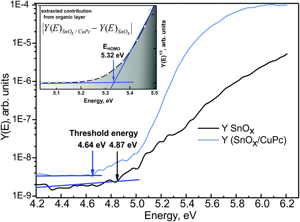 | ||
Fig. 6 PYS spectrum recorded for bare SnOx ( ) and SnOx/CuPc structure ( ) and SnOx/CuPc structure ( ). The threshold energies were determined assuming a linear background. The inset presents extracted CuPc contribution to the overall signal, fitted with a linear function for determination of the HOMO level of CuPc; the Y-axis scale “power” is the consequence of Kane's model assumption.59 The shadowed area under the curve indicates the increasing density of occupied states. ). The threshold energies were determined assuming a linear background. The inset presents extracted CuPc contribution to the overall signal, fitted with a linear function for determination of the HOMO level of CuPc; the Y-axis scale “power” is the consequence of Kane's model assumption.59 The shadowed area under the curve indicates the increasing density of occupied states. | ||
Subtracting the oxide layer signal from the SnOx/CuPc layered structure signal, it is possible to determine the contribution to the quantum yield from the organic overlayer. Next, plotting the resulting signal where according to Kane's theory n = 3 for organic semiconductors,59 and fitting it with a linear function,58 it is possible to determine the HOMO energy of the examined organic layer. The procedure is presented in the inset to Fig. 6. This procedure yields EHOMO = 5.32 eV for CuPc. The EF–EHOMO energy separation then follows as 0.68 eV.
The above is consistent with the increase of the photoemission yield after CuPc deposition. The relatively weak photoemission from SnOx is due to fact that the probed energy region is the band gap energy range with only a minor number of occupied energy states. After CuPc deposition, the probed energy region is embracing the occupied energy states from the CuPc valance band (states below EHOMO), hence there is significant number of additional states that can be excited by ultraviolet radiation.
All of the information drawn from both photoemission experiments allows drafting the band-like diagram showing the depth-related changes in the electronic structure of the examined bilayer system, as well as the energy level alignment at the SnOx/CuPc interface (Fig. 7). The diagram is based on the assumption of an aligned Fermi level between the sample's layers and the measurement equipment. The right-hand-side depth scale at the bottom of the diagram is quantitative for information depth only for the organic layer owing to the limitations of the procedure to extract depth described above. The left-hand side related to SnOx is only semiquantitative to distinguish regions farther from or closer to the SnOx/CuPc interface.
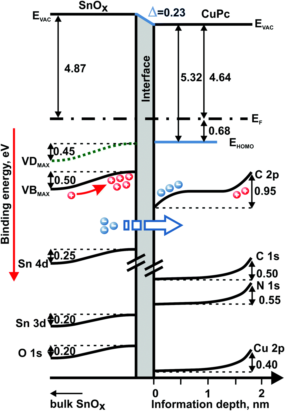 | ||
| Fig. 7 Band-like diagram presenting depth-dependent variations in energy level alignment for the investigated SnOx/CuPc structure drawn on the basis of two photoemission experiments. All presented values in eV. EF – Fermi level position. | ||
The interface dipole is clearly visible with the drop in the vacuum level in Fig. 7. The shape of the changes in energy position of the particular energy levels at the both sides of the interface points to charge transfer via the SnOx/CuPc interface as the most probable cause of the energy level shift. As a consequence, the oxide suffers significant hole accumulation near the interface while the organic layer exhibits electron accumulation at the opposite side of the interface.
The behavior of the energy levels is consistent with the reverse bias model proposed by Renshaw and Forrest for inorganic/organic heterojunctions.60 In this model, the carrier current was dominated by Shockley–Read–Hall generation in the depletion region of the inorganic oxide, and minority carrier diffusion took place into the inorganic layer and majority carrier transfer towards the organic layer. Hence, we assume that the most probable and dominating effect here is the electron transfer from the oxide layer to the organic film. At the organic side of the interface, the charge transfer causes a downward shift of the CuPc energy levels, as manifested by the first kink of the C 2p level. “First” refers to the position seen from the interface. The magnitude of the shift corresponds to the VB level shift at the oxide side. The charge transfer assumption is highly probable here since the pinning of the HOMO level energy position (which could prevent the charge transfer) is unlikely here as was described for similar systems before.49,61 The energy shift of the C 2p level near the ambient surface possesses a different origin. According to our experience with air-exposure-related processes in CuPc, the energy shift near the surface should be related to oxygen uptake, which induces an upward energy level shift of the CuPc's shallow energy levels.62
The smaller magnitude of the oxide's deep core levels energy shift can be explained by the fact that SnOx valance levels are more susceptible to charge transfer effects than the core levels. This difference in sensitivity might be caused by screening effects.63
An open question concerns the role of the defect levels in the electronic processes taking place at the SnOx/CuPc interface. According to our last study28 and theoretical predictions made by Varley, Granato and Togo,46,64,65 defect states are surface-related features and in their majority should be treated as electron donor states. It is obvious from the band diagram that the defect states are lowering the EF–EV energy distance. Hence, defects can reduce the charge injection barrier by changing the density of the occupied states distribution.66 However, are they the centers of charge transfer? The different behavior of the VD and VB levels could give a hint in this direction. Analyzing the data from Fig. 5(b) in their representation in Fig. 7, we can observe that the VB levels are becoming energetically more localized towards the interface. Interfacial localization of the VB levels is supported by (i) absence of a depth-dependent difference in the VDmax–VDonset energy separation, and (ii) the change in the VBmax–VBonset energy separation. Consequently, the hypothesis is self-evident that the VB plays a key role in the charge transfer process, while VD states augment charge transfer by reducing the charge injection barrier. The explanation of the VB narrowing could be that according to the charge transfer multiplet theory,67 the core hole potential created after the charge transfer leads to significant energy variations of different occupied energy states. This in turn might yield shape change of particular peaks representing occupied states in photoemission experiment, and in particular may lead to the observed narrowing of the VB component in this work.
Conclusions
An ultra-thin inorganic/organic hybrid structure has been analyzed within this work. The heterojunction based on SnOx and CuPc was characterized in detail, and its electronic structure and chemical composition have been determined.The obtained heterojunction exhibited a high degree of purity with minor carbon and oxygen contamination. The in-depth chemical analysis pointed that the majority of the carbon contamination remains near the bottom of the sol–gel-derived SnOx layer as a residual of the manufacturing process. A slight oxygen-related contamination was found to be placed at the inorganic/organic interface.
The organic ultra-thin film in the investigated SnOx/CuPc structure drastically increases the photoemission yield from the examined SnOx-based structure. Photoemission allowed determination of the SnOx work function as 4.87 eV in the absence of an organic layer, and its drop to 4.64 eV after deposition of an organic layer. The latter value was assigned to the CuPc work function in the examined system. The change of the work function by 0.23 eV was attributed to the existence of an interface dipole, manifested as the drop of the vacuum level position. The interface dipole is most probably caused by a charge transfer via the SnOx/CuPc interface. The interrogation of the core levels confirmed this charge displacement description.
Quantitative analysis of core and valance energy levels revealed that the SnOx valance levels are more susceptible to charge transfer effects than the deep core levels: O 1s, Sn 3d shifted ∼0.20 eV, while VB shifted ∼0.50 eV. Differences in shifts might be also affected by screening effects. The charge transfer in the presence of an organic overlayer is manifested most intensively in the position of nitrogen-related core levels. However, the magnitude of CuPc's shallow energy level changes led to the conclusion that the C 2p levels are playing the key role in the charge transfer process owing to being a part of the CuPc's aromatic system. In the oxide layer, the VO and VSn defect levels are supposed to augment the charge transfer by reducing the charge injection barrier. Moreover, the CuPc layer suffered a surface-related energy level shift, which was likely caused by oxidation. This was especially observable in a second C 2p shift and a core level shift at the vicinity of CuPc surface.
Information obtained with the conducted experiments allowed construction of a band-like diagram, presenting energy level alignment at the SnOx/CuPc interface.
The presented results prove the applicability of lab-based angle-dependent and energy-resolved photoemission methods for non-destructive analysis of the buried interface energy structure. In addition, determination of charge-related phenomena taking place at inorganic/organic junctions was demonstrated. This is of importance for ultra-thin layer technology of perspective inorganic–organic hybrid electronic devices as well as for fundamental and comprehensive understanding of physical and chemical processes at such interfaces.
Acknowledgements
This work was partially supported by the Polish budget for science in years 2013–2015 by the Ministry for Science and Higher Education within Iuventus Plus IP2012 019072 project through the Silesian University of Technology, Institute of Physics. L. G. would like to acknowledge support of the Institute of Physics – CSE through statutory funds BK-243/RIF/2016. A. S. thanks Maxnet Energy for support. Special thanks go to Prof. Jerzy Bodzenta and Prof. Andrzej Bluszcz for continuous support.References
- A. Balandin, Nat. Mater., 2011, 10, 569 CrossRef CAS PubMed.
- N. Chen, C. Huang, W. Yang, S. Chen, H. Liu, Y. Li and Y. Li, J. Phys. Chem. C, 2010, 114, 12982 CAS.
- Characterization of Semiconductor Heterostructures and Nanostructures, ed. C. Lamberti and G. Agostini, Elsevier, Amsterdam, 2013 Search PubMed.
- S. K. Saha, A. Guchhait and A. J. Pal, Phys. Chem. Chem. Phys., 2014, 16, 4193 RSC.
- S. K. Saha, A. Guchhait and A. J. Pal, Phys. Chem. Chem. Phys., 2012, 14, 8090 RSC.
- J. M. Luther, M. Law, M. C. Beard, Q. Song, M. O. Reese, R. J. Ellingson and A. J. Nozik, Nano Lett., 2008, 8, 3488 CrossRef CAS PubMed.
- A. Guchhait and A. J. Pal, J. Phys. Chem. C, 2010, 114, 19294 CAS.
- J. Androulakis, C. Lin, H. Kong, C. Uher, C. Wu, T. Hogan, B. Cook, T. Caillat, K. Paraskevopoulos and M. Kanatzidis, J. Am. Chem. Soc., 2007, 129, 9780 CrossRef CAS PubMed.
- L. Wang, M.-H. Yoon, G. Lu, Y. Yang, A. Facchetti and T. J. Marks, Nat. Mater., 2006, 5, 893 CrossRef CAS PubMed.
- G. Li, R. Zhu and Y. Yang, Nat. Photonics, 2012, 6, 153–161 CrossRef CAS.
- W. Li, A. Furlan, K. H. Hendriks, M. M. Wienk and R. A. Janssen, J. Am. Chem. Soc., 2013, 135, 5529–5532 CrossRef CAS PubMed.
- Y. Idota, T. Kubota, A. Matsufuji, Y. Mackawa and T. Miyasaka, Science, 1997, 176, 1395 CrossRef.
- N. Tsuda, Electronic Conduction in Oxides, Springer Science & Business Media, 2000 Search PubMed.
- Y. S. Zhang, D. X. Wang, Z. Y. Wang and Y. Y. Wang, Opt. Quantum Electron., 2016, 48, 18 CrossRef.
- O. A. Melville, B. H. Lessard and T. P. Bender, ACS Appl. Mater. Interfaces, 2015, 7, 13105 CAS.
- C. D. Dimitrakopoulos and P. R. L. Malenfant, Adv. Mater., 2002, 14, 99 CrossRef CAS.
- P.-L. Ong and I. A. Levitsky, Energies, 2010, 3, 313 CrossRef CAS.
- A. S. Komolov, S. A. Komolov, E. F. Lazneva, A. A. Gavrikov and A. M. Turiev, Surf. Sci., 2011, 605, 1452 CrossRef CAS.
- A. S. Komolov, S. A. Komolov, E. F. Lazneva, A. A. Gavrikov and P. S. Repin, Tech. Phys., 2012, 57, 256 CrossRef CAS.
- S. Sinha and M. Mukherjee, J. Appl. Phys., 2013, 114, 083709 CrossRef.
- M. Batzill, K. Katsiev and U. Diebold, Appl. Phys. Lett., 2004, 85, 5766 CrossRef CAS.
- T. B. Fleetham, J. P. Mudrick, W. Cao, K. Klimes, J. Xue and J. Li, ACS Appl. Mater. Interfaces, 2014, 6, 7254 CAS.
- T. Fleetham, B. O'Brien, J. P. Mudrick, J. Xue and J. Li, J. Appl. Phys., 2013, 103, 083303 Search PubMed.
- G. Bersuker, C. S. Park, J. Barnett, P. S. Lysaght, P. D. Kirsch, C. D. Young, R. Choi, B. H. Lee, B. Foran, K. van Benthem, S. J. Pennycook, P. M. Lenahan and J. T. Ryan, Appl. Phys. Lett., 2006, 100, 094108 Search PubMed.
- M. Krzywiecki and L. Grządziel, Appl. Surf. Sci., 2014, 311, 740 CrossRef CAS.
- J. G. Van Dijken and M. J. Brett, Molecules, 2012, 17, 10119 CrossRef CAS PubMed.
- Y. Gao, Mater. Sci. Eng., R, 2010, 68, 39 CrossRef.
- M. Krzywiecki, A. Sarfraz and A. Erbe, Appl. Phys. Lett., 2015, 107, 231601 CrossRef.
- http://www.casaxps.com .
- I. Lindau, P. Pianetta, K. Y. Yu and W. E. Spicer, Phys. Rev. B: Solid State, 1976, 16, 492 CrossRef.
- R. L. Opila and J. Eng Jr., Prog. Surf. Sci., 2002, 69, 125 CrossRef CAS.
- http://www.thermoscientific.com/en/product/theta-probe-angle-resolved-x-ray-photoelectron-spectrometer-arxps-system.html .
- P. Seah and W. A. Dench, Surf. Interface Anal., 1979, 1, 2 CrossRef.
- C. J. Powell and A. Jablonski, NIST Electron Inelastic-Mean-Free-Path Database, Version 1.2, SRD 71, National Institute of Standards and Technology, Gaithersburg, MD, 2010 Search PubMed.
- W. S. M. Werner, Surf. Interface Anal., 1992, 18, 217 CrossRef CAS.
- S. Tanuma, C. J. Powell and D. R. Penn, Surf. Interface Anal., 1993, 21, 165 CrossRef.
- P. J. Cumpson, Surf. Interface Anal., 2000, 29, 403 CrossRef CAS.
- J. R. Taylor, An Introduction to Error Analysis: The Study of Uncertainties in Physical Measurements, University Science Books, Sausalito, 1997 Search PubMed.
- D. Ehre and H. Cohen, Appl. Phys. Lett., 2013, 103, 052901 CrossRef.
- A. Rozenblat, Y. Rosenwaks, L. Segev and H. Cohen, Appl. Phys. Lett., 2009, 94, 053116 CrossRef.
- A. Givon and H. Cohen, Surf. Interface Anal., 2015, 47, 607 CrossRef CAS.
- L. Grządziel, M. Krzywiecki, G. Genchev and A. Erbe, Synth. Met., 2017, 223, 199 CrossRef.
- L. Grządziel and M. Krzywiecki, Synth. Met., 2015, 210B, 141 CrossRef.
- D. A. Evans, H. J. Steiner, S. Evans, R. Middleton, T. S. Jones, S. Park, T. U. Kampen, D. R. T. Zahn, G. Cabailh and I. T. McGovern, J. Phys.: Condens. Matter, 2003, 15, S2729 CrossRef CAS.
- A. Walsh, D. J. Payne, R. G. Egdell and G. W. Watson, Chem. Soc. Rev., 2011, 40, 4455 RSC.
- J. B. Varley, A. Schleife, A. Janotti and C. G. Van de Walle, Appl. Phys. Lett., 2013, 103, 082118 CrossRef.
- http://xpssimplified.com/elements/tin.php .
- X. Liu, D. Zhang, Y. Zhang and Xi. Dai, J. Appl. Phys., 2010, 107, 064309 CrossRef.
- M. T. Greiner, M. G. Helander, W.-M. Tang, Z.-B. Wang, J. Qiu and Z.-H. Lu, Nat. Mater., 2012, 11, 76 CrossRef CAS PubMed.
- http://www.lasurface.com .
- R. Pilolli, N. Ditaranto, N. Cioffi and L. Sabbatini, Anal. Bioanal. Chem., 2013, 405, 713 CrossRef CAS PubMed.
- C. R. Brundle, G. Conti and P. Mack, J. Electron Spectrosc. Relat. Phenom., 2010, 178–179, 433 CrossRef CAS.
- M. Arndt, J. Duchoslav, H. Itani, G. Hesser, C. K. Riener, G. Angeli, K. Preis, D. Stifter and K. Hingerl, Anal. Bioanal. Chem., 2012, 403, 651 CrossRef CAS PubMed.
- Hollemann-Wiberg: Lehrbuch der Anorganischen Chemie, De Gruyter, Berlin, 101st edn, 1995.
- H. Cohen, C. Nogues, I. Zon and I. Lubomirsky, Appl. Phys. Lett., 2005, 97, 113701 Search PubMed.
- T. Chasse, C. I. Wu, I. G. Hill and A. Kahn, J. Appl. Phys., 1999, 85, 6589 CrossRef CAS.
- M. Krzywiecki, L. Ottaviano, L. Grządziel, P. Parisse, S. Santucci and S. Szuber, Thin Solid Films, 2009, 517, 1630 CrossRef CAS.
- Electronic Processes in Organic Electronics; Bridging Nanostructure, Electronic States and Device Properties, Springer Series in Materials Science, ed. H. Ishii, K. Kudo, T. Nakayama and N. Ueno, Japan, 2015, vol. 209 Search PubMed.
- E. O. Kane, Phys. Rev., 1962, 127, 131 CrossRef CAS.
- C. K. Renshaw and S. R. Forrest, Phys. Rev. B: Condens. Matter Mater. Phys., 2014, 90, 045302 CrossRef.
- L. Ley, Y. Smets, C. I. Pakes and J. Risten, Adv. Funct. Mater., 2013, 23, 794 CrossRef CAS.
- L. Grządziel and M. Krzywiecki, Thin Solid Films, 2014, 550, 361 CrossRef.
- T. C. Taucher, I. Hehn, O. T. Hofmann, M. Zharnikov and E. Zojer, J. Phys. Chem. C, 2016, 120, 3428 CAS.
- D. B. Granato, J. A. Caraveo-Frescas, H. N. Alshareef and U. Schwingenschlogl, Appl. Phys. Lett., 2013, 102, 212105 CrossRef.
- A. Togo, F. Oba, I. Tanaka and K. Tatsumi, Phys. Rev. B: Condens. Matter Mater. Phys., 2006, 74, 195128 CrossRef.
- A. Klein, C. Korber, A. Wachau, F. Sauberlich, Y. Gassenbauer, S. P. Harvey, D. E. Proffit and T. O. Mason, Materials, 2010, 3, 4892 CrossRef CAS.
- F. de Groot and A. Kotani, Core Level Spectroscopy of Solids, CRC Press, Taylor & Francis Group, Boca Raton, 2008 Search PubMed.
| This journal is © the Owner Societies 2017 |