
 Open Access Article
 This Open Access Article is licensed under a Creative Commons Attribution-Non Commercial 3.0 Unported Licence
Doping of RE ions in the 2D ZnO layered system to achieve low-dimensional upconverted persistent luminescence based on asymmetric doping in ZnO systems
Bolong
Huang

Department of Applied Biology and Chemical Technology, The Hong Kong Polytechnic University, Hong Hum, Kowloon, Hong Kong SAR, China. E-mail: bhuang@polyu.edu.hk
First published on 19th April 2017
Abstract
Herein, we dope a low-dimensional ZnO system with a wide range of rare earth (RE) ions. Through systematic calculations, the dopable range of all ZnO systems was found to be asymmetrical, which accounts for the difficulty in achieving p-type doping. Low-dimensional ZnO systems, similar to 2D graphene-like nanosheets, have a wider doping limit. Thus, 2D ZnO is a promising candidate to achieve a wider doping range in ZnO. To further examine energy transfer in upconversion luminescence, the excited states of all lanthanide (Ln) elements in both the Ln2+ and Ln3+ ionic state in the bulk ZnO lattice were extensively studied. The probability of mixed valences of the Ln dopant ions occurring in ZnO was discussed, along with the analysis of the relative oscillator strengths. At the Ln2+ states, the heavy lanthanide elements usually dominated the energy transmission channel at high energy, the medium lanthanide elements mostly occupied the middle range of the optical fundamental gap, and the light lanthanide elements were widely spread over the optical band gap as well as the conduction band range. However, Ln3+ ions, as the sensitizing dopant, have reduced energy barriers for excited state absorption, showing wider energy transfer channels that are evenly distributed within 3.0 eV, which is lower than the conduction band edge absorption in Ln2+. Meanwhile, each energy level has an obviously stronger oscillator strength, indicating a larger probability for excitation and energy transport between the inter-levels. Thus, in physicochemical and biological terms, trivalent Ln doping follows the removal of apical dominance concept, contributing more flexible energy transfer within the biological window for in vivo imaging or other related optoelectronic devices.
Introduction
ZnO, a transparent semiconducting oxide, has a wide band gap of 3.4 eV with a large exciton binding energy of 60 meV1 and exhibits strong size-dependent electronic and optical properties. Currently, scientific interest in the flexibility and the size- and shape-controlled fabrication of nanomaterials is growing. Low-dimensional ZnO nanostructures have great potential for human-friendly nanodevices, biomedical science, and light-emitting devices that require extremely low power consumption.2–4 Multi-scaled, low-dimensional ZnO, which can be produced using various novel fabrication technologies, has promising applications in solid-state, short-wavelength, light-emitting, transparent, conducting, and piezoelectric materials, as well as in room-temperature ultraviolet (UV) laser emission devices and UV photovoltaic cells with tailored dimensions.5–9 Due to its biocompatibility and luminescence, which is often applied in biomedical science, ZnO has potential in biophotonics and biomedical applications for imaging living cells and tissue.10Recent experiments have shown that ZnO exhibits both two-photon absorption (TPA) and two-step two-photon absorption (TS-TPA) photon upconversions (UCs) with a tunable and energy-efficient UC mechanism that persist even at low excitation density.11,12 These pioneering experiments shed light on opportunities for modulating and improving the output luminescence and device applications of ZnO nanomaterials.
UC has rapidly attracted great research interest in a number of fields, with a focus on applications such as bioprobes, drug delivery, tumor positioning in anti-cancer research, and optoelectronics.11–24 Ln3+-doped or Ln3+-based UC nanoparticles (UCNPs) are of great interest for bioprobes, as they respond to a wide range of stimuli13–18 and are superior to conventional quantum dots and organic dyes, whose luminescence is sensitive to their size and chemical surroundings.4,19–21 Due to their near infrared (NIR) emission and deep penetration depths by long wavelengths, UCNPs offer minimized photodamage, high signal-to-noise ratios and remarkable penetration depths for in vitro and in vivo applications,22–27 bioprobes,19,28 and drug delivery29,30 in biological chemistry and in biomedical treatment/therapy in anti-cancer research.19,22,26,31–36 The biosafety of UCNPs is relatively stable, as determined by biotests,26,37 and UCNPs present low nanotoxicity, as noted in a recent review.38 In addition, UCNPs also exhibit promising applications in solar cells due to their enhanced energy conversion efficiency resulting from their ability to absorb solar light in the infrared region.39 Combinatorial approaches have recently been developed to quickly screen UCNP candidates for biological applications via high-throughput screening, modeling and applications using tailored 96-well microplate parallel synthesis systems.40
In fact, native energy transfer events in Ln3+-doped UCNPs dominate the UC efficiency,21 and the high-throughput synthesis and screening of applicable UCNP candidates leads developments to remain in the experimental trial phase, as different energy transfer pathways may vary the output color of UC emissions because emission can proceed via various photoelectron transport mechanisms.41 However, energy transfer studies can manipulate the UC through guided theoretical energy transfer mechanisms to achieve satisfactory efficiency and the desired output color.
Epitaxial techniques are considered promising methods for producing ZnO thin films for optoelectronic devices. In comparison with conventional vapor-phase deposition methods, solution-deposition techniques, such as chemical bath deposition (CBD), have attracted attention because of their low-cost setup, low processing temperature, high productivity, and scale-up potential, especially for ZnO thin films grown on glass substrates.25 Moreover, if the substrate is pre-seeded with ZnO crystallites or a small amount of transition metal ions, such as Fe2+ or Fe3+, drawbacks of CBD, such as the irreproducible heterogeneous growth of the ZnO film, can be overcome.26–28
The microemulsion-mediated hydrothermal approach is another convenient route. A number of remarkable studies have reported that Zn(OH)42− and Zn(NH3)42+ can be used as precursors in solution and have detailed simple strategies to obtain tunable, multi-scaled, low-dimensional ZnO nanomaterials.29–35 Zero-dimensional (0D) nanoparticles as well as two-dimensional (2D) nanoplates or nanosheets can be obtained via the oriented attachment mechanism under hydrothermal conditions by the following synthetic pathway:29–35

Following the above route, well-crystallized and monodisperse nanoparticles can be obtained through Ostwald ripening. This synthetic strategy exhibits certain flexibility in controlling the morphology and can tune the dimension of ZnO to either one-dimensional (1D) or 2D nanocrystals. Hao et al. also attempted a similar route, obtaining a different morphology.35
Here, we emphasize that intermediates in the synthesis of layered structural materials can act as generalized precursors, and outline a universal synthetic method to obtain 2D ultrathin nanomaterials, which can be applied to obtain ZnO with a 2D layered structure.36 The findings recently reported by Yan et al.36 not only allow the fabrication of a controllable ultrathin 2D nanomaterial but also contribute a cornerstone material for related fundamental studies on the properties and performances of these materials, as well as the future exploration of new materials through this facile synthetic route.
To date, the energy levels of lanthanide (Ln) dopants in ZnO-related nanomaterials, including the thermodynamic transition levels, single-particle levels, and excitation levels, have not been thoroughly studied. In particular, the nature and mechanism of emission induced by different energy transfer events via Ln2+ in the ZnO system has not been well interpreted through theoretical studies. Therefore, it is necessary to explore and understand the intrinsic dopable range of lanthanide ions and the excitations that lead to specific UC energy transfer properties.
The n-type doping of ZnO can be achieved through electronic modulation, while p-type doping is very difficult to achieve.37,38 One of our collaborators suggested that this difficulty may be due to asymmetric doping behavior resulting from native point defects, especially oxygen vacancies (VO) and zinc vacancies (VZn).39,40 Synthesized ZnO usually presents intrinsic n-type semiconducting behavior,41,42 which may be due to intrinsic defects or hydrogen (H) atoms produced during synthesis.43,44
Bulk ZnO materials typically have two common crystal phases: zincblende or wurtzite. Both phases show direct band structures at the Γ point of the Brillouin zone (BZ).45 However, the optoelectronic applications of these materials are affected by their limitations in p-type doping. These limitations arise from native point defects, which control the boundary of the bi-polar doping limit (n-/p-doping limit) and are largely composed of intrinsic lattice defects, such as vacancies or interstitials.37 The Fermi level cannot be easily modified by extrinsic dopants due to the spontaneous formation of numerous native point defects, which influences the n-/p-doping limit.39
Other lattice systems can be fabricated, such as the rock-salt lattice, which can be obtained under high pressures of approximately 9–10 GPa, and the 2D graphene-like ZnO lattice, which can be obtained using molecular beam epitaxial growth or the microemulsion hydrothermal method. Moreover, amorphous semiconductor thin films, such as amorphous ZnO (am-ZnO), have relaxed k-selection rules and optical transition constraints, endowing these materials with unique advantages over crystalline thin films or bulk materials. Additionally, the sample preparation of am-ZnO has a lower cost and can be amended to produce large-area sheets or thin films.46 Furthermore, solid am-ZnO shows a better light conversion efficiency and improved energy transitions between inter-level excitations. Herein, we perform a preliminary study on the intrinsic dopable range in am-ZnO.
To study the persistent luminescence of ZnO, the defect process and dynamics under external photoirradiation must be understood. Charge transfer and energy transport must be interpreted via accurate calculations of the energy levels with and without doping (e.g., n- or p-type doping).47,48 On the other hand, these calculations require a systematic study of a range of native point defect levels in terms of the single-particle levels (SPL), thermodynamic transition levels (TTL), and optical vertical excitation levels under the Franck–Condon framework.48 Moreover, to estimate the energy formation cost, note that native point defects depend on the specific chemical potential limit and the local structural relaxation and cross-section of defects that capture charge carriers. Our recently developed model shows that the long-decay recombination behavior of excited electron–hole pairs occurs through a time-accumulated donor–acceptor band, which has been continuously pumped by local lattice distortions with a corresponding negative effective correlation energy.49–51 Our model not only combines a lattice relaxation model resulting from defects such as DX and EL2 centers52,53 and an energy barrier model involving the photogenerated Coulomb potential from electron–hole pairs,54–56 but also shows a potential zero-phonon line electronic inter-band transition, which can explain the energy conversion mechanism leading to persistent luminescence.
To achieve a better combination of experimental observations and theoretical studies, electronic structure calculations are necessary for each given ZnO system. As is well known, the electronic structure of a given semiconductor material plays a significant role in determining its potential applications. Correct band structures and defect levels are important for experimentalists engaging in defect engineering to tune the electronic properties through extrinsic doping. However, the doping limits determined by the native point defect levels are still unknown. Therefore, we herein extend the doping limit study to several ZnO systems to determine how the doping limit varies with the symmetry and dimension of ZnO solid systems via density functional theory (DFT) calculations.
Calculation setup
Ground state structure optimization
Our defect-state structural relaxation and formation energy calculations were performed using the CASTEP code.57 Norm-conserving pseudopotentials of Zn and O were generated by the OPIUM code in the Kleinman–Bylander projector form,58 which employs a non-linear partial core correction on the fully closed 3d10 shell59 and a scalar relativistic averaging scheme60 to account for spin–orbital coupling effects. The Rappe–Rabe–Kaxiras–Joannopoulos (RRKJ) method was chosen to optimize the pseudopotentials.61 The PBE functional was chosen for PBE+U calculations, with a kinetic cutoff energy of 750 eV, which expands the valence electron states in a plane-wave basis set. The ensemble DFT (EDFT) method of Marzari et al.62 was used for convergence when considering the am-ZnO system. To obtain the bulk properties of WZ-ZnO, we used a 9 × 9 × 6 Monkhorst–Pack (MP) k-point mesh, where the total energy convergence of each atom was under 5.0 × 10⁻⁷ eV. For the electronic structure calculations of the 2D layered ZnO system, we examined a 4 × 4 × 1 supercell after the total energy convergence calculations using our developed pseudopotentials63 with a 750 eV cutoff energy. The Hellmann–Feynman force on each atom was converged to lower than 0.01 eV Å−1. To calculate the defects in am-ZnO, we used a simple cubic cell containing 64 atoms. We selected the (¼, ¼, ¼) special k-point64 in the simple cubic cell. Geometry optimizations used the Broyden–Fletcher–Goldfarb–Shanno (BFGS) algorithm through all bulk and defect supercell calculations.Hubbard-U ab initio determination at each Zn and O site
As determined in the theoretical studies, the electronic and localized defect states that occur in the optical fundamental gap were less sensitive to the nonlinearity or orbital coupling of Hubbard U parameters. Thus, the rotational-invariant DFT+Hubbard U (DFT+U) method was used, which follows the Anisimov-type approximation.65 To remove side effects of the localized hole states produced by the 2p orbitals of O sites, the self-consistently determined Hubbard U potentials were also applied to the O-2p orbitals, which is a common practice66–69 for many oxide materials. Therefore, self-energy corrections of both the d- and p-orbitals of the various forms of zinc oxides, especially the amorphous structures, must be considered.63,70–72 We have carried out series of ab-initio calculations on the on-site orbital Coulomb potential parameter (i.e. Hubbard U) in any given structures. This process returns the self-consistent parameters on each Zn and O sites based on our previously developed method.71,72Defect formation enthalpy formula
We used the equation developed by Zunger et al.73 to calculate the defect formation energy at different charge states (q). The overall supercell was established and remained fixed for all lattice parameters based on the ground state relaxed primitive cell to reduce the effect of enthalpy changes resulting from cell variations. The formation energy of a target defect (Hq) at a specific charge state q can be described as the relation between the Fermi energy level (EF) and the chemical potential Δμ of defect species α, which is described as follows: | (1) |
 is the reference chemical potential of the element α.
Charge point defect corrections within the periodic lattice
In the case of defects with q ≠ 0, a Coulomb potential correction is required to counteract the effects from the image charge of the crystal lattice. To date, three corrections have been developed. One is the band alignment correction developed by Van de Walle and coworkers.74 The second is the dispersion correction of defects between the gamma point and Monkhorst–Pack point, developed by Wei et al.75 The third is the dipole correction, which considers the Madelung effect based on static electric Coulomb potential corrections, developed by Makov and Payne;76 this method is the current popular correction scheme in DFT and is used by us in this work. However, such image charge corrections contribute only around ∼0.2 eV in magnitude to the defect formation energy. Our goal is to establish a physicochemical trend, rather than highly accurate level calibrations, which require demanding computations.Results and discussion
Ground state electronic properties
We first examined the electronic structures of ZnO in different lattice systems and compared the band structures of wurtzite (WZ), zincblende (ZB), rock-salt (RS) and 2D monolayer ZnO, as shown in Fig. 1. RS ZnO was shown to have an indirect minimum band gap from L → Γ of the BZ, where the conduction band minimum (CBM) is at the Γ point. This arises because the O sites have 6-fold octahedral coordination, which deviates from the common 4-fold tetrahedral coordination of WZ-ZnO, as shown in Fig. 1. The O-2p orbitals have largely re-distributed energy levels along the new BZ in RS ZnO, compared with WZ ZnO. Therefore, the VBM of RS-ZnO, which mainly consists of O-2p orbitals, is different from that of WZ ZnO and does not occur at the Γ point.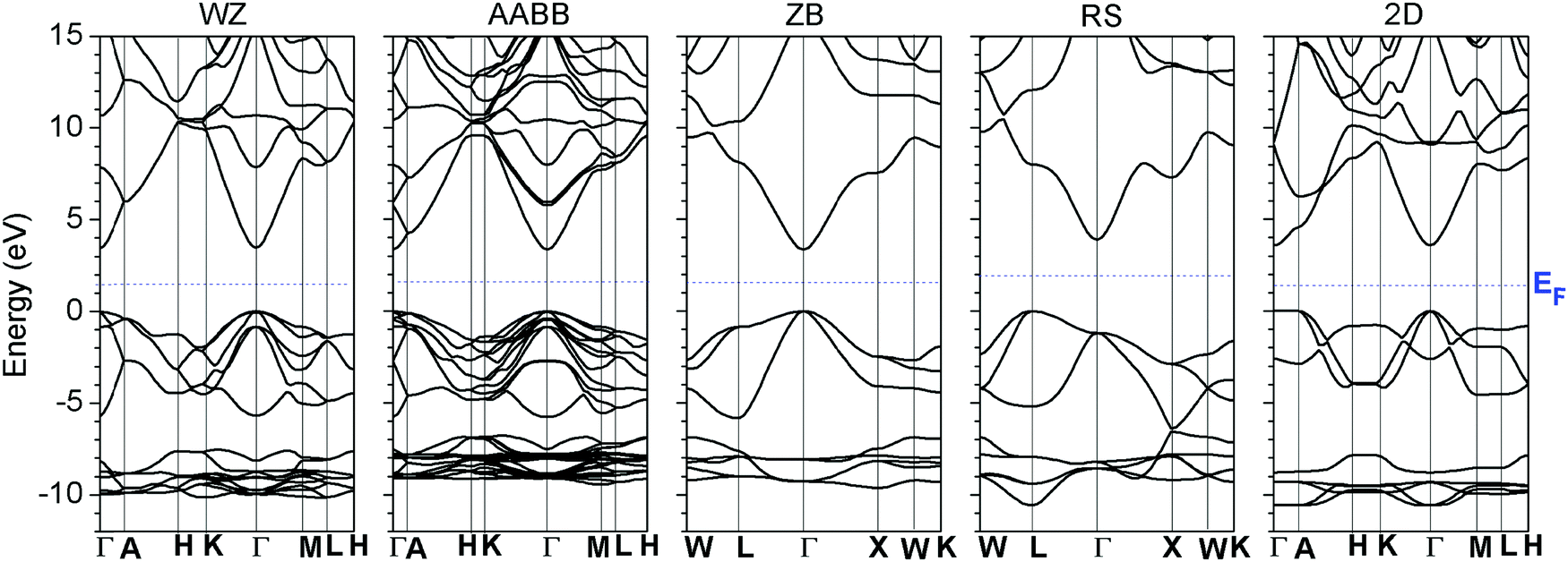 | ||
| Fig. 1 The calculated band structures of wurtzite (WZ), AABB, rock-salt (RS), and two-dimensional monolayer (2-D) ZnO systems. | ||
Fig. 2 shows the total electronic density of states (DOS) of ZnO in the different lattice systems. We further introduced an am-ZnO model for comparison. Both ZB and RS ZnO present van Hove singularities at the Zn-3d t2g levels, showing ∇kE = 0 near the highly symmetrical L → Γ → X points. In the amorphous system, the long-range order of the Zn and O sites is lost, while the local structures maintain short-range bonding angles and lengths similar to those of the ZnO single crystal. Thus, the Zn-3d t2g levels of am-ZnO appear as broadened and less intense peaks, starting from 6.8 eV below the VBM.
 | ||
| Fig. 2 The calculated total density of states (TDOSs) of wurtzite (WZ), AABB, zinc-blend (ZB), rock-salt (RS), amorphous (am) and two-dimensional monolayer (2-D) ZnO systems. | ||
As the electronic properties of WZ ZnO with native point defects have been studied in previous works,40,77 we further examined the formation energies of native point defects in relation to the Fermi level (EF) of WZ ZnO under different charge states and chemical potential limits, which is typically done when considering the formation energies of native point defects. For comparison with other calculation methods using hybrid-functional DFT,40,78 the formation enthalpy ΔHf of WZ ZnO is −3.67 eV, which is much closer to the experimental data of −3.60 eV at 300 K. The direct band gap was found to be 3.44 eV from the band structure calculation based on the method we developed71,79 using the new pseudopotential for Zn, as discussed in our previous report,63 and the Zn-3d t2g level started from 7.1 eV below the VBM (EV −7.1 eV).
Native point defects and dopable range in WZ ZnO
As seen in Fig. 3(a), the formation energy of oxygen vacancies (VO) is 0.98 eV in the neutral state under the O-poor limit, which gives a reasonable prediction of the defect concentration at approximately 900 K and is consistent with experimental data.80,81 The defect with the second lowest formation energy is zinc interstitials (IZn), with a value of 3.84 eV, and the (+/0) transition level within the conduction band (CB) is located at EV +4.21 eV, where EV = 0 at the VBM. IZn is a possible donor source that provides charge carriers by donating electrons. However, in our calculations, the formation energy of IZn in the neutral state is relatively high and is nearly 2 eV higher than that of VO. Meanwhile, VO does not provide any mobile charges and instead contains strongly bound electrons that possess a negative Ueff (Ueff = −0.65 eV), showing a spin-paired correlation that cannot be detected by electron spin resonance (ESR) measurements.82 Moreover, V2+O and I2+Zn have almost the same formation energy trends in relation to EF, indicating their similar behavior as defect trap centers within the ZnO lattice. This finding implies that most experimental research has misunderstood the role of VO and IZn as donor centers due to their similar behavior.81,82Fig. 3(b) shows that VZn and IO are negatively charged defects with relatively low formation energies of 3.16 eV and 2.97 eV, respectively, under the O-rich limit. These defect sites also present negative Ueff features with −1.04 eV and −1.58 eV, respectively. | ||
| Fig. 3 Summary of native point defects in WZ-ZnO in O-poor (a) and O-rich (b) chemical potential limits. Summary of doping limits determined by native point defects in both O-poor (c) and rich (d) limits, denoted by green arrows. | ||
Next, we considered the doping limit in WZ ZnO, as shown in Fig. 3(c). When EF is raised to the CBM by a donor dopant, the n-type doping limit (upper bound) is the point at which negatively charged native point defects spontaneously form to compensate for the charge. Thus, either VZn or IO determines the n-type limit energy level. Considering the band gap area, VZn has a neutral formation energy similar to IO. However, due to the shallower (0/2−) transition level at EV +0.67 eV compared with that of IO, V2−Zn shows enhanced stability within the band gap area. Therefore, EF = EV +4.09 eV is the critical point at which V2−Zn spontaneously forms to compensate for the n-type dopant under the O-poor limit, while the critical point is EF = EV +2.25 eV under the O-rich limit.
Similarly, for p-type dopants (acceptors), EF is lowered to the VB edge EV, and as EF varies, donor defects, such as VO and IZn, will spontaneously form to compensate for the charge if relatively low formation energies are reached. Accordingly, in the O-poor limit, the lower bound of the doping limit is determined by V2+O due to its slightly lower formation energy in the band gap area compared with I2+Zn. Therefore, the p-type limit energy levels are 2.53 eV and 0.21 eV. Note that Robertson et al. showed that the lower bounds of the EF area are 1.80 eV and 0.20 eV, respectively.39 This difference arises in the O-poor limit because the formation energy of VO, determined by the pure Zn-rich chemical limit, is relatively low in the neutral state at 0.85 eV, which is 0.1 eV lower than most of the reported DFT calculation results.42,83 The source of error may be the formation enthalpy of −3.37 eV given previously,39,40 which is 0.32 eV higher than that found experimentally. Compared with our calculated values of 4.09 eV and 2.25 eV for the n-type limit at different chemical potential limits, their source of error results from their formation energies of VZn at the various charge states being too high, which led to a wider range for the upper bound of the doping limit (n-type limit).40 We have discussed doping limits in other systems, which were then used to achieve persistent luminescence via doping.84
The RS ZnO system does not have a doping limit at which to tune the Fermi level pinning boundary by extrinsic doping. Moreover, this system has an indirect band gap, which lowers the optical vertical transition efficiency via k-selection rules. Thus, this system was not considered.
Native point defects in amorphous ZnO
We then examined continuous random ZnO networks (CRN-ZnO) as more realistic am-ZnO models. For this work, we built short-range disordered ZnO in a 64-atom supercell using the RS ZnO lattice. The RS structure has many possible distortion directions, and there are many ways to generate distorted ZnO models. The building and generation of an amorphous model structure is an art in and of itself, as summarized by Drabold et al., and usually requires equilibration over long time periods to achieve dynamic randomization and geometry relaxation at 0 K to guarantee that high-energy features of the structural configuration are mostly absent.85 Am-ZnO structures have many potential applications. Thus, there are numerous generation paths for modeling the amorphous structures, which means there may be no universal method for generating amorphous metal oxide materials for a specific purpose. Falk et al. showed a recent example with a much more elaborate generation of am-ZnO structures.86Ab initio molecular dynamics (MD) are typically used to model experimental environments. Here, am-ZnO was obtained using MD simulations with a 64-atom supercell (Zn32O32). First, the volume of the ideal 64-atom RS ZnO cell was held constant using the experimentally reported density, and the cell was melted at 1500 K for 2.5 ps (time interval of 1 fs). Second, the supercell was simulated at 600 K for 1 ps to represent an annealing process. Third, the model was further simulated at 300 K for 4 ps to obtain thermal equilibrium. The final structure was obtained after geometry relaxation by varying the cell size at the ground state. In the final structure, the weighted average coordination numbers of Zn and O were 3.6 and 3.5, respectively. Nearly 44% of the Zn sites were 4-fold coordinated with tetrahedral configuration, and nearly 50% of the O sites had tetrahedral configuration. The Zn and O coordination numbers of am-ZnO were lower than those of WZ-ZnO at around 3.
We next considered native point defects in am-ZnO, as well as their influence on the electronic properties. By projecting each orbital component of the electrons in the defective systems, we illustrated the partial density of states (PDOS) of am-ZnO with oxygen and zinc vacancies at different charge states.
As seen in Fig. 4(a) and (b), the difference in the coordination of the O vacancies leads to localized defect states with slightly different depths. The higher the VO coordination number, the deeper the donor-like trap levels within the band gap. The 4-fold coordinated O vacancy (VO4) has a trap level of EV +2.17 eV, where EV = 0 at the VBM, while VO3 has a defect trap level of EV +2.29 eV. Moreover, the localized defect states are contributed by the components of the p- and s-orbitals of the two electrons on the adjacent 3 or 4 Zn sites. Compared to V0O in the WZ ZnO system, the trap levels of VO4 and VO3 in am-ZnO are 0.1–0.2 eV deeper than the trap level in WZ ZnO (EV +2.38 eV) according to our PDOS calculations. Moreover, the perturbed hole states (PHSs) are approximately 0.2 eV below the CBM, similar to the results of Lany and Zunger.48
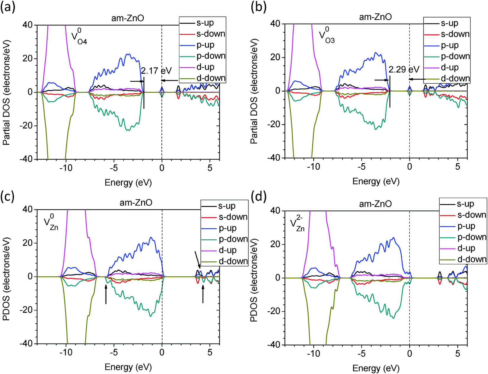 | ||
| Fig. 4 The calculated partial DOSs (PDOSs) of am-ZnO with VO4 (a) and VO3 (b) in neutral states. The PDOSs of am-ZnO with VZn in neutral (c) and −2 charge (d) states. | ||
Fig. 4(c) and (d) shows the two different charge states of VZn in am-ZnO. The neutral Zn vacancy (V0Zn) in am-ZnO indeed acts as an extra deep acceptor next to the CB edge (0.2 eV higher than the CBM), with contributions from the two different p-orbitals of the hole states localized on the adjacent O atoms. Similarly, V0Zn in WZ ZnO is located at the CB edge. For V−Zn in the am-ZnO system, the localized hole state is reported to be localized on only one of the adjacent O sites or delocalized over the system, depending on the calculation level and modeling of the self-energy of the electrons in the orbitals.63,71,79,84 V2−Zn in am-ZnO captured two electrons in the neutral state of the defect, acting as an acceptor-like trap.80 In Fig. 4(d), the two captured electrons are localized right up to the VBM with energy intervals of approximately 0.1 eV due to contributions from the components of the p- and partially filled d-orbitals of the adjacent Zn and O sites.
Fig. 5 shows the charge density of the above defects in am-ZnO in different charge states. The relaxations of adjacent Zn ions next to VO in am-ZnO are illustrated by arrows, indicating a strong Coulomb repulsive interaction of each nearby Zn ion when the localized electrons are ionized away (V2+O in am-ZnO). V0Zn in ZnO induces two localized hole states in the p-orbitals of two adjacent O sites in different spin-up and spin-down configurations, respectively. The charge density of V−Zn confirms that the single localized hole is present in the p state at only one of the adjacent O sites, which is consistent with the results of Clark et al.40 In the V2−Zn state of am-ZnO, two additional electrons fill not only the p-orbitals of the O sites but also the d-orbitals of the second nearest neighboring Zn sites; thus, the charge density of V2−Zn shows the co-existence of p- and d-orbitals of the localized states.
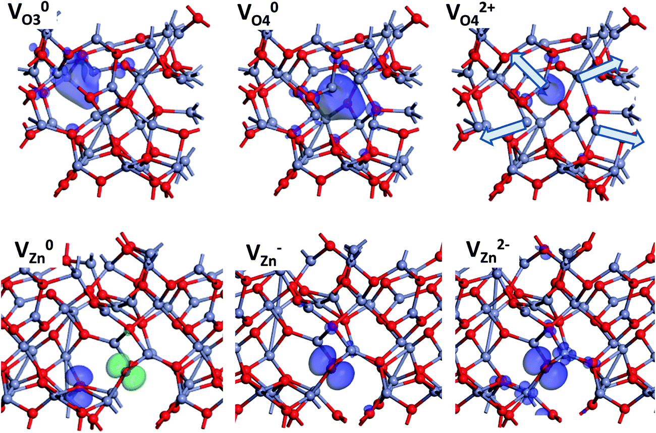 | ||
| Fig. 5 Charge density of the 3-fold and 4-fold coordinated oxygen vacancy (VO3 and VO4) for its neutral and 2+ charge states. The relaxation of Zn ions is indicated by arrows. Charge density of the Zn vacancy (VZn) for its neutral (with spin-up and spin-down), 1−, and 2− charge states. The charge density of V−Zn is a p-state localized on only one of the adjacent oxygen atoms (Zn = grey and O = red). | ||
2D monolayer ZnO system
As is well known, ZnO is a wide-band-gap semiconductor oxide with a direct gap of approximately 3.4 eV (at 300 K), and its monolayer can be used as a charge trapping layer in CMOS memory cells. Recently, many studies have shown that low-dimensional ZnO nanomaterials can be synthesized and present promising potential in renewable energy or electronics applications, for example, the near 0D quantum dot synthesized by Dutta et al.,87 the 1D nanowire synthesized by Hwang et al.,88 and the 2D nanolayer synthesized by Lau et al.89 The physicochemical trends of the 2D ZnO system have shown that 2D ZnO can be tuned to be both n- and p-type, presenting doping flexibility.89 Moreover, the formation stability of the ideal 2D monolayer ZnO system has been studied and predicted by first-principles calculations.90–93 Meanwhile, interfacial charge transfer between monolayer ZnO and graphene is a promising method for 2D electronic modulation with application in high-speed electronic response devices.As shown in Fig. 6(a) and (b), the band structure and density of states show tail states due to the absence of long-range crystal field interactions vertically along ZnO(0001), and the 3d levels are split into two peaks due to an evident difference in p–d coupling along and perpendicular to ZnO(0001). The band gap increased to 3.57 eV, in comparison to the bulk phase value of 3.44 eV, which was determined from our calculations. The start of the 3d level is 0.5 eV deeper than that in the bulk (i.e., −7.0 eV by calculation). The formation entropy of bulk ZnO is −3.70 eV, which is consistent with the experimentally reported value of −3.60 eV at 300 K. Fig. 1 and 2 give the basic electronic properties of bulk WZ and monolayer ZnO, respectively.
 | ||
| Fig. 6 (a) TDOS of the monolayer ZnO system with intrinsic neutral Zn vacancy (V0Zn). (b) Formation energy vs. Fermi energy within different charge states of 1−, 0, and 1+, for VZn in monolayer ZnO. (c) Localized orbitals electron and oxygen hole states near the valence and conduction band edges within charge states of 1−, 0, and 1+ (Zn = grey, O = red, spin-up hole state = pink, spin-down hole state = green, and spin-up and spin-down electrons = golden and blue). (d) Schematic diagram illustrating the decrease of energy as the symmetry is reduced from D3h to D2h, and the Dirac-cone levels pinned in the mid-gap of the host monolayer ZnO within the system of graphene/monolayer ZnO. | ||
The oxygen hole levels in metal oxides and wide-band-gap semiconductors have long been of interest, particularly those in ZnO,94,95 where the localized hole levels drive the Fermi level deeper in the gap. We investigated a single zinc vacancy (VZn), as this state can induce two holes localized at nearby O sites. However, this state cannot be clearly modeled by LDA/GGA calculations, as the homogeneous electron gas treats the two hole states as degenerate and delocalized around the VZn site. Our GGA+U calculation stabilizes the hole states and produces clear electron–hole interactions under different charge states, as shown in Fig. 6(a). This result has also been reported in our previous works.63,70,71,79,84Fig. 6(b) shows that neutral VZn has a negative effective correlation U (negative Ueff) value of −0.57 eV for the process of 2(V0Zn) → (V+Zn) + (V−Zn). Such exothermal reaction indicates that one of the O sites, which are the nearest neighbors of V0Zn, acted as an acceptor, capturing two electrons and easily overcoming the onsite Coulomb repulsive energy. The other two localized hole states were repulsive, while the electron acceptor sites moved towards the hole sites. This behavior induces a planar Jahn–Teller distortion effect, where the symmetry is reduced from D3h to D2h. The other two charge states, V+Zn and V−Zn, also show the same trend. The total energy of the system decreases during the structural relaxation. As seen in Fig. 6(c), the localized hole states have π-like orbitals near the CBM that are perpendicular to the (0001) plane in real space, showing pz-orbital character (with a1 symmetry). However, the electron acceptor site has a similar π-like orbital along the (0001) plane, which is a feature of the pxy-orbital. This interesting behavior gives the monolayer ZnO system with the existence of a single neutral VZn antiferromagnetic (AFM) features.
We also found that the hole and electron levels are not free-charge-carrier supply centers but are instead localized trap states. The intrinsic conductivity of monolayer ZnO may largely be restricted by such native defects. The EF was actually pinned near the midgap. If we interface the system with a graphene layer, the position of the Dirac cone (cone apex level) will be pinned near the midgap of ZnO, owing to subtle electron–hole interactions (illustrated in Fig. 6(d)). This behavior can be understood by considering two extreme points in the CBM and VBM of the ZnO–graphene hybrid system. The electrons of the ZnO host lattice are delocalized, but the holes are bound and localized in the CB, while in the VB, the electrons are bound and the holes are freely delocalized. The Dirac cone apex level denotes the 2D free electron gas (from the graphene system) without the effective mass and presents the largest mobility, where electrons at that level are constrained in the graphene system. This means that in such 2D hybrid systems, competing interactions in the Coulomb potential are counteracted or balanced at the midgap where the cone level is located.
Additionally, Jahn–Teller distortion occurs in monolayer ZnO with VZn because the asymmetry between the occupancy of the pxy and pz orbitals within the planar monolayer ZnO is larger than that in non-centrosymmetric bulk WZ ZnO. This asymmetry can also be found in ZnO but is negligible.95
Doping limit in amorphous, 2D, and AABB ZnO
We further examined the amorphous and 2D monolayer ZnO systems. As seen in Fig. 7(a) and (b), the amorphous system has a doping range that is similar to that of WZ ZnO between the p- and n-type doping limit, which are 1.23 eV and 1.56 eV for amorphous and WZ ZnO, respectively. Remarkably, the p-type doping limit in the O-rich chemical potential of am-ZnO shifted to the VB edge and overlapped with the EF below the VBM. In the O-poor limit, the p-type doping limit is approximately EV −0.26 eV (0.26 eV below the VBM), which is contributed by the positive doubly charged, 4-fold coordinated O vacancy (V2+O4) in am-ZnO. The only difference in the 3-fold coordinated O vacancy is in the formation energy at the neutral state in the O-poor limit, which is 1.36 eV and 0.80 eV for V0O4 and V0O3, respectively. Though V2+O3 is almost the same as V2+O4, V2+O3 shows a positive Ueff with a value of Ueff = +0.86 eV, indicating the possibility of detection by ESR measurement. V2+O4 has a relatively small negative Ueff of −0.13 eV, which is 20% of that of WZ ZnO. Thus, the amorphous structure not only possesses distorted Zn and O sites with randomly varied coordination but also reduces the Anderson-type effective spin correlation effect of multi-electrons at the same atomic site, leading to a reduced negative effective correlation energy (−Ueff) or even turning to the positive value. | ||
| Fig. 7 Summary of doping limits of amorphous ZnO (a and b), 2D ZnO (c and d) and AABB ZnO (e and f) determined by the native point defects in both O-poor and O-rich limits, denoted by green arrows. | ||
V2−Zn has an n-type doping limit of 3.02 eV and 1.45 eV in the O-poor and O-rich limit, respectively. Note that the n-type doping limit in the O-poor limit deviated from the CB edge, showing lower n-type conductivity achieved by extrinsic donor dopants, such as AlZn. This indicates that am-ZnO can potentially easily adopt a p-type dopant under the O-rich limit, while still showing n-type dopable behavior under the O-poor limit because the n-type boundary overlaps with the CB. Therefore, am-ZnO has a bi-polar doping capability depending on the chemical potential limit, but the dopable range is relatively small compared to that of WZ-ZnO, due to the n-type limit shifting away from the CB.
Another important system is 2D ZnO, which consists of pure 3-fold coordinated Zn and O sites with a honeycomb lattice. As seen in Fig. 7(c) and (d), the dopable range increased from 1.56 eV to 3.13 eV. The variation in the doping limit under different chemical potential limits is very similar to the behavior of WZ ZnO. The p-type limit begins at EV +2.01 eV and EV +0 eV in the O-poor and O-rich limit, respectively, as determined by V2+O. The n-type doping limit was determined by V2−Zn and was EV +5.14 eV and EV +3.13 eV in the O-poor and O-rich limit, respectively. Our calculations show the physicochemical trend that 2D ZnO can undergo p-type doping. Moreover, an experimental study showed that a similar system can undergo both n- and p-type doping for flexible modulation of the doping behavior.89
From Fig. 7(e) and (f), AABB-type stacking in ZnO shows a similar doping limitation as that in the WZ lattice. In the O-poor limit, the EF range without the spontaneous formation of native point defects spans from EV +2.45 eV to EV +4.10 eV. This range also overlaps with the CB, which is consistent with the conclusion that ZnO is an intrinsic n-type dopable solid system. In the O-rich limit, the dopable EF range spans from EV +0.13 eV to EV +1.78 eV. This range is closer to the VBM than that calculated for the WZ system. However, this range still shows that this system has less flexibility for p-type doping than the am-ZnO and 2D ZnO systems discussed above. Thus, modulation of the 3D lattice stacking in bulk ZnO does not substantially improve the range to achieve p-type doping.
In contrast, GaN has a wide doping range, although it is also a wide-band-gap semiconductor like ZnO. GaN can be easily doped by both n-type and p-type dopants over its wide band gap area, while ZnO possesses asymmetric doping features, except in the 2D ZnO system. Most structures, such as WZ, ZB and am-ZnO, present only good overlap with the CB edge in the O-poor chemical limit, corresponding to the intrinsic n-type behavior of ZnO, and the EF can be easily tuned by a donor dopant near the CB edge. However, the p-type limit shows that the EF cannot be easily shifted towards or overlap the VB edge; thus, p-type doping is rather difficult to achieve in ZnO, as ZnO possesses an asymmetric dopable range according to the different chemical potential limits (Table 1).
| Band gap | Formation enthalpy | V0O (O-poor) | V0Zn (O-rich) | |
|---|---|---|---|---|
| WZ | 3.444 | −3.667 | 0.975 | 3.164 |
| RS | 3.883 | −3.377 | 1.361 | 2.227 |
| Am | 3.250 | −3.133 | 1.364/0.804 | 3.536 |
| 2D | 3.570 | −3.061 | 0.810 | 2.909 |
Wide selection and dopable range for rare earth (RE) ions in the 2D ZnO system
ZnO is a transparent semiconducting oxide with a wide band gap of 3.4 eV and can accommodate a wide range of RE ion dopants to modulate the output luminescence. Based on the above calculations and discussions, we found that the 2D 3-fold symmetrically arranged ZnO layered structure can adopt a relatively wide dopable range compared to the 3D bulk ZnO system. Therefore, it is highly desirable to conduct a preliminary theoretical study on RE ion doping and the related electronic states and properties. In this study, we mainly considered the RE2+ doping level. This study gives not only a theoretical reference for modulating the output luminescence via UC energy transfer but also theoretical guidance for future applications of low-dimensional, RE ion-doped, persistent phosphor luminescence materials.We divided the RE elements doped in the ZnO system by their RE separation level: La, Ce, Pr, Nd, and Pm (radioactive) are the light RE elements; Sm, Eu, Gd, Tb, and Dy are the medium RE elements; and finally, Ho, Er, Tm Yb, and Lu are the heavy RE elements.
For the light RE elements, we first looked at the La-doped 2D ZnO system, as shown in Fig. 8(a). Substitution of the neutral La dopant at the Zn site (La0Zn) gives a localized electronic state with an s-orbital component near the CBM at EV +3.0 eV (EV denotes the position of the VBM). This accords with the fact that the 6s2 electrons in the valence orbitals of RE ions are the most easily ionized. The s-orbital electrons are donated into the system and aligned in a filled state below the CBM. Both the 5d and 4f states are above the CBM, and the CB in the system shows ferromagnetic (FM) spin alignment. The localized states are EV +6.3 eV and EV +7.2 eV, respectively. Doping with the singly positively charged species (La+Zn) induces AFM behavior, and EV +6.0 eV and EV +6.6 eV for the 5d and 4f empty states, respectively. Meanwhile, the top of the valence band of the ZnO host lattice is also slightly modified. For the doubly positively charged doping state (La2+Zn), the localized hole state remains at EV +0.3 eV above the VBM. The empty 5d and 4f levels produced by the La dopant slightly change to EV +6.3 eV and EV +6.9 eV, respectively. The top of the valence band is similar to that in the La0Zn system but with slight FM behavior.
 | ||
| Fig. 8 The projected partial density of states of light rare earth (RE) elements doped in 2D-ZnO layer structure (light RE: La, Ce, Pr, Nd, and Pm). (a) LaZn, (b) CeZn, (c) PrZn, (d) NdZn and (e) PmZn. | ||
In the Ce-doped 2D ZnO system (Fig. 8(b)) at the Ce0Zn doping state, the 6s2 electronic state occupies the EF level (EV +3.2 eV) below the CBM, and the 4f filled state is 0.2 eV below the EF, or EV +3.0 eV. The localized 4f empty states are at EV +6.2 eV in spin-up configuration and at EV +7.0 eV in spin-down configuration, showing FM spin alignment. The 5d empty states are nearly delocalized at EV +6.8 eV and EV +7.2 eV in the spin-up and spin-down configurations, respectively. For the Ce+Zn state, the 4f filled state is localized at EV +1.8 eV within the band gap of the ZnO host system and occupies the EF of the whole system, and the level of the s-orbital is 0.4 eV above this EF level. The 4f empty state in spin-up configuration is at EV +5.1 eV, and in the spin-down configuration is at EV +5.8 eV. The spin-up configuration of the 5d level is relatively more distinguishable and is found at EV +5.9 eV. In the Ce2+Zn state, the system shows AFM behavior in the 4f and 5d spin alignments. The 4f states are all empty and localized at EV +1.8 eV above the VBM, and the empty 5d levels are even higher at EV +5.0 eV, approximately 1.5 eV above the CBM.
In the Pr-doped ZnO system, the neutral doping state (Pr0Zn) shows a localized 4f filled state at 1 eV above the VBM (EV +1.0 eV) that is located near the midgap, as shown in Fig. 8(c). The EF is also aligned with the s-orbital level. In the CB region, the localized 4f empty states have four levels with two spin-up orientations at EV +5.7 eV and EV +6.2 eV, while the spin-down levels are at EV +7.4 eV and EV +8.4 eV. The localized 5d empty states remain at EV +6.5 eV and EV +6.8 eV. The Pr+Zn state of ZnO shows a localized 4f filled state 0.2 eV below the VBM (EV −0.2 eV). The 4f empty states with spin-up configuration remain at EV +4.5 eV and EV +5.2 eV, while the spin-down states are at EV +5.8 eV and EV +6.3 eV. In the Pr2+Zn state, the 4f empty states are well distributed within the band gap of the host ZnO system. The spin-up configuration of the empty 4f localized levels remains at EV +0.4 eV and EV +0.7 eV, while the spin-down levels are localized at EV +2.1 eV and EV +3.2 eV. All of the localized 5d empty states are located at higher levels than the 4f orbitals, which remain at EV +4.5 eV and EV +5.1 eV.
In the Nd-doped 2D ZnO system, as shown in Fig. 8(d), the neutral state (Nd0Zn) shows a localized 4f filled state at 4.0 eV below the VBM (EV −4.0 eV) that is buried within the valence band. As is known, the valence band mainly consists of O-2p orbitals of the ZnO system. The 4f empty states are 5.8 above the VBM (EV +5.8 eV) in the spin-up configuration and at EV +7.9 eV and EV +9.0 eV in the spin-down configuration. The 5d empty states remain at EV +6.3 eV and EV +7.0 eV. For the Nd+Zn state, all of the 4f levels are shifted to lower energies. The filled 4f orbitals are at EV −4.8 eV, while the empty 4f orbitals are at EV +4.9 eV in the spin-up state and at EV +7.1 eV and EV +8.2 eV in the spin-down state. The 5d levels are localized at EV +5.8 eV and EV +6.2 eV. In the 2+ charge state of NdZn doping (Nd2+Zn), a shallow hole state is localized at 0.2 eV above the VBM (EV +0.2 eV), occupying the p-orbitals of O sites. The localized 4f filled level remains at EV −4.8 eV below the VBM, which is almost unchanged from that of the 1+ state. The 4f empty states show a slight difference and are localized in the CB at EV +5.2 eV in the spin-up configuration and at EV +7.3 eV and EV +8.4 eV in the spin-down configuration. The 5d empty levels accordingly remain at EV +6.1 eV and EV +6.5 eV.
The element Pm is radioactive. Although it is unsafe to actualize Pm-doping in ZnO, we still investigated the electronic properties of its doping in the 2D ZnO layered system, as shown in Fig. 8(e). In the Pm0Zn state, the 4f filled state is localized at EV −5.3 eV below the VBM in the spin-up configuration. The corresponding empty states are localized at EV +5.8 eV in the spin-up configuration and at EV +8.6 eV and EV +9.8 eV in the spin-down configuration. The 5d-orbital levels overlap with the 4f empty states at EV +6.3 eV and EV +7.2 eV. In its 1+ charge state (Pm+Zn), the 4f filled level shifts to EV −6.3 eV. The 4f empty states are at EV +4.8 eV in the spin-up configuration and at EV +7.5 eV and EV +8.6 eV in the spin-down configuration. The 5d levels are localized at EV +5.7 eV and EV +6.2 eV. For the 2+ charge state (Pm2+Zn), the 4f filled level is at EV −6.1 eV. Similarly, the doping state produces a localized hole state at approximately 0.2 eV above the VBM, contributed by the p-orbitals. The 4f empty states remain at EV +5.1 eV in the spin-up configuration and at EV +7.8 eV and EV +8.9 eV in the spin-down configuration. The localized 5d levels shift to EV +6.0 eV and EV +6.6 eV.
For the medium RE elements, Sm doping shows a behavior that is different from that of the light RE elements (Fig. 9(a)). In the neutral state (Sm0Zn), the 4f filled orbitals show a wider energetic range spanning from EV −4.0 eV to EV −6.0 eV, which overlaps with the O-2p orbitals. The empty states of the 4f orbitals remain at EV +9.6 eV and EV +10.6 eV in the spin-down configuration and are at EV +5.5 eV in the spin-up configuration. The 5d orbitals of Sm0Zn remain at EV +6.2 eV and EV +7.5 eV. Sm+Zn doping gives 4f filled states localized below the VB, in contrast to the neutral state. The two peaks remain at EV −5.3 eV and EV −6.0 eV. The empty states of the 4f orbitals are located at EV +4.6 eV in the spin-up configuration and at EV +8.2 eV and EV +9.5 eV in the spin-down configuration. The 5d orbitals are intermediate between the 4f empty states and are localized at EV +5.5 eV and EV +6.4 eV. For Sm2+Zn doping in the ZnO system, the 4f filled state is localized in the range of EV −4.8 eV to EV −6.5 eV. The shallow hole state is localized at 0.2 eV above the VBM in the spin-down configuration. The 4f empty state is 4.9 eV above the VBM in the spin-up configuration, while the spin-down states remain at 8.6 eV and 9.9 eV above the VBM. The spin-up and spin-down states of the 5d orbital are located at 5.8 eV and 6.8 eV above the VBM, respectively.
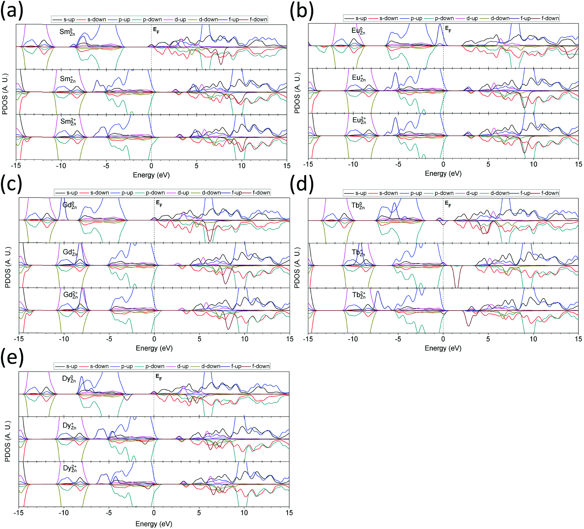 | ||
| Fig. 9 The projected partial density of states of medium rare earth (RE) elements doped in 2D-ZnO layer structure (medium RE: Sm, Eu, Gd, Tb, and Dy). (a) SmZn, (b) EuZn, (c) GdZn, (d) TbZn and (e) DyZn. | ||
In Eu-doped ZnO, shown in Fig. 9(b), the 5d–4f level transition leads to red emission through dipole energy transfer. In the neutral state (Eu0Zn), the 4f filled state shifts higher than the VB of ZnO, indicating that the 4f occupied orbital levels are energetically higher than the 2p orbitals of the O sites in the host materials, which are at EV +0.5 eV. In the singly positively charged state (Eu+Zn), the 4f filled states are below the VBM with a slight overlap, remaining at EV −5.3 eV and EV −6.2 eV. In the doubly positively charged state (Eu2+Zn), the 4f filled states are almost unchanged, where the empty states remain at EV +2.8 eV and the lowest 5d level remains at EV +5.3 eV. The energetic interval between the 4f empty state and the 5d state ranges from EV +3.2 eV to EV +5.2 eV, which affords red emission at 610 nm due to electronic de-excitation from 4f65d1 to 4f7.
With increased electronic occupation of the 4f orbitals, the 4f filled state of Gd further lowers and begins to overlap with the t2g component of the 3d10 orbitals of the Zn sites, as shown in Fig. 9(c). Meanwhile, due to the repulsive Coulomb potential, the t2g level of the 3d10 orbital shifts to a lower level compared to that in the undoped ZnO system. In this doping system, Gd0Zn contributes to the 4f filled state at EV −7.2 eV below the VBM, while only one 4f empty state is present at EV +8.2 eV above the VBM. The 5d levels occupy positions in the CB at EV +6.2 eV and EV +7.7 eV, showing FM behavior. In the Gd+Zn state, the 4f filled level overlaps with and is buried into the 3d10 orbitals of the Zn sites. This behavior arises because the positive charge state weakens the shielding effects of the valence shell of the Gd sites due to the reduced 6s2 environment, thus leading to a stronger repulsive interaction between the Gd-4f and O-2p orbitals and reaching EV −8.2 eV. The 5d empty state is localized within the ZnO band gap at EV +2.6 eV, and another two levels are located at EV +5.3 eV and EV +6.8 eV, overlapping with the CB of ZnO. The 4f empty state is found to be EV +7.9 eV above the VBM. In the Gd2+Zn state, the behavior of the 4f filled state is similar to that of the singly positively charged state, but the level is raised by 0.4 eV to EV −7.8 eV. Similarly, a localized shallow hole state results from the p-orbitals of the O sites of ZnO at 0.2 eV above the VBM. The localized 5d level in the band gap shifts to a higher energy of EV +2.9 eV, and the other two levels remain at EV +5.6 eV and EV +7.2 eV in the CBM. Meanwhile, the 4f empty state is also 0.3 eV higher (EV +8.2 eV) than that in the Gd+Zn state.
The Tb-doping ZnO system (Fig. 9(d)) shows a different behavior from the Gd-doped system discussed above, especially in the 4f positions of both the filled and empty states. In the neutral doping state, Tb0Zn in ZnO leads to a 4f filled state localized within the valence band of ZnO contributed by the O-2p orbitals, which is EV −3.3 eV below the VBM. However, this state does not contribute to the electronic transitions via energy transfer because parity selection forbids p–f transitions. Furthermore, other 5d and 4f filled states are also found to be localized within the band gap of ZnO at EV +1.7 eV and EV +2.2 eV in the spin-up and spin-down configuration, respectively. The 4f empty states overlap with the CB at EV +6.5 eV and EV +7.0 eV, both in the spin-down configuration. The 5d empty states remain high at EV +7.7 eV, EV +8.3 eV and EV +9.8 eV. In the Tb+Zn doping state, the 4f filled state shifts lower to EV −9.3 eV and overlaps with the 3d10 orbitals of the Zn sites. The EF level is pinned at the VBM with a localized 5d-orbital contributed by the Tb site. The 4f empty state is localized near the midgap with an energy of EV +1.5 eV. This behavior is completely different from that of the other medium RE elements but similar to that of the Ce-doped system. The 5d states are located at EV +5.1 eV and EV +7.0 eV in the CB. In the Tb2+Zn doping state, the 4f filled states are intermediate between the 3d10 and 2p orbitals, with twin peaks at EV −6.2 eV and EV −7.2 eV in the spin-up configuration. The EF is also pinned near the VBM in the range of EV to EV +0.05 by two 4f orbital levels, one filled and the other empty. The filled 4f state remains at the VBM, and the empty 4f state is hybridized with the neighboring O-2p orbitals, contributing a shallow hole level localized near the VBM. Therefore, Tb2+Zn in ZnO may be a good shallow acceptor. The empty states of the 4f orbitals remain near the CBM, with levels of EV +2.8 eV and EV +3.6 eV in spin-down alignment. The 5d levels are located at EV +5.2 eV and EV +6.6 eV.
In the Dy-doped system, as shown in Fig. 9(e), the 4f filled states are widely spread over the valence band and band gap, which is consistent with our previous work on the CaS system.84 In the neutral state (Dy0Zn), the lowest two 4f filled states overlap with the bottom of the VB at EV −4.2 eV and EV −5.2 eV. The third 4f filled state occupies the VBM at 3.0 eV below the EF level. The 5d filled level partially occupies the EF level, while the empty state is located at EV +6.2 eV. Meanwhile, the 4f empty states remain at EV +7.0 eV and EV +7.7 eV. For the Dy+Zn state, the lower three 4f filled states partially overlap with the O-2p orbitals at the bottom of the VB and remain at intermediate levels between the O-2p and Zn-3d orbitals at EV −4.5 eV, EV −5.6 eV and EV −6.2 eV, all in the spin-up configuration. The highest occupied 4f orbital level is in the VB range at EV −1.0 eV below the VBM in the spin-down configuration. The 5d levels remain in the gap at EV +2.8 eV and in the CB at EV +5.8 eV and EV +6.7 eV. The 4f empty states are also in the CB at EV +6.2 eV and EV +7.2 eV in the spin-down configuration. For the Dy2+Zn doping state, the 4f filled levels are slightly different from those in the 1+ charge state, which are EV −0.7 eV, EV −4.2 eV, EV −5.3 eV and EV −5.9 eV below the VBM. A shallow hole state is localized on the p-orbital of the O sites at 0.3 eV above the VBM. The 5d level is localized at EV +3.2 eV below the CBM. The higher energy levels are located at EV +6.2 eV and EV +7.1 eV in the CB. The 4f empty levels remain at EV +6.5 eV and EV +7.6 eV in the spin-down configuration.
We next examine the doping of heavy RE elements in ZnO, beginning with Ho (Fig. 10(a)). All the 4f filled states show the physical trend of lower energy levels resulting from increased 4f occupations. In the neutral state (Ho0Zn), the 4f filled states are located below the VBM, with one in the VB at EV −3.0 eV and two between the Zn-3d and O-2p orbitals at EV −5.3 eV and EV −6.4 eV. The 4f empty state is localized at EV +7.0 eV between the two localized 5d empty states, which are located at EV +6.9 eV and EV +7.8 eV. In the Ho+Zn doping state, the 4f filled states are localized at the lower energy levels of EV −4.2 eV, EV −6.5 eV, and EV −7.6 eV. The 4f-emtpy states remain at EV +5.6 eV and EV +6.2 eV. The 5d empty states are localized at EV +6.0 eV and EV +6.8 eV. In the Ho2+Zn doping state, the 4f filled states are shifted to a slightly higher energy range and are located at EV −3.9 eV, EV −6.1 eV, and EV −7.3 eV. The 4f empty states remain at EV +6.0 eV and EV +6.6 eV. The 5d orbitals are localized as empty states at EV +6.5 eV and EV +7.1 eV.
 | ||
| Fig. 10 The projected partial density of states of heavy rare earth (RE) elements doped in 2D-ZnO layer structure (heavy RE: Ho, Er, Tm, Yb, and Lu). (a) HoZn, (b) ErZn, (c) TmZn, (d) YbZn and (e) LuZn. | ||
Er doping in ZnO provides interesting results, as shown in Fig. 10(b). In the neutral doping state (Er0Zn), the 4f filled states show similar behavior to those in the Ho-doped system. The filled levels are localized at EV −1.3 eV, EV −2.5 eV, and EV −3.0 eV. For the empty states in the CB of ZnO, the 4f empty state is localized at EV +8.8 eV in the CB, while the 5d states remain at EV +6.8 eV and EV +7.5 eV. For the Er+Zn doping state, the 4f filled states are shifted down to EV −4.4 eV, EV −6.0 eV, and EV −7.1 eV. The 4f empty state is localized at EV +7.6 eV. The 5d levels remain at EV +6.0 eV and EV +6.5 eV. For the Er2+Zn doping state, the 4f filled states are even lower than the 3d10 level of Zn in the ZnO system and are localized at EV −10.0 eV, EV −12.4 eV, and EV −13.6 eV. The 4f empty states are well localized within the band gap and range from EV +0.5 eV and EV +2.4 eV. The 5d states are also localized within the band gap at EV +0.4 eV above the VBM. Another three 5d states remain at EV +3.6 eV, EV +4.4 eV, and EV +5.6 eV. This doping state (Er2+Zn) may actualize NIR emission at a wavelength of approximately 654 nm (i.e., photon energy of 1.9 eV). This energy transfer is primarily accomplished by the two localized d states within the band gap. As is known, the d–d transition is parity disallowed. However, the noncentrosymmetric local lattice of the RE dopant will relax the selection rule for electronic transitions. Fig. 10(b) shows the substantial p–d orbital overlap within the band gap at EV +0.4 eV above the VBM. At the same time, the ZnO lattice system possesses an inherent noncentrosymmetric atomic arrangement. Thus, electronic transitions under external photoirradiation, such as UV light, will occur resulting in higher level d orbitals at EV +3.6 eV. Upon overcoming the small energy barrier, the excited electrons can flip to a spin-down configuration (or the spin direction of the excited electrons can be reversed). Then, a triplet electronic de-excitation occurs between the higher energetic 5d level and the lower energy level of the 4f empty state. The direct minimum energetic interval of such de-excitation ranges from 1.7 eV to 1.9 eV, which is in good agreement with the experimentally suggested potential of the 654 nm NIR output emission.
The Tm-doped ZnO system, shown in Fig. 10(c), has no localized states within the band gap. In the neutral doping state (Tm0Zn), the 4f filled states largely overlap with the O-2p band (VB). The states are localized at EV −3.4 eV, EV −4.0 eV, EV −4.5 eV, and EV −5.7 eV. The 5d states are localized at EV +7.0 eV and EV +7.4 eV. The 4f empty state is localized at EV +7.3 eV. In the Tm+Zn state, the 4f filled states are localized below the VBM at EV −5.2 eV, EV −5.6 eV, and EV −6.9 eV in the spin-up configuration and at EV −3.6 eV, EV −4.3 eV, and EV −4.8 eV in the spin-down configuration. The 4f empty states remain at EV +6.2 eV, and the 5d states are localized at EV +6.3 eV and EV +6.6 eV. For the Tm2+Zn doping state, the localized states of the 4f and 5d orbitals are similar to those in the +1 charged state. The 4f filled states are localized at EV −3.4 eV, EV −4.2 eV, and EV −4.6 eV in the spin-down configuration and at EV −4.8 eV, EV −5.3 eV and EV −6.4 eV in the spin-up configuration. The shallow hole state is contributed by the distorted O sites occupying 2p orbitals at 0.2 eV above the VBM. The 4f empty state remains at EV +6.5 eV, and the 5d levels remain at EV +6.6 eV and EV +7.0 eV.
In Yb-doped ZnO (Fig. 10(d)), the 4f filled states are widely distributed within the valence band, which consists of O-2p orbitals, as seen in the neutral doping state (Yb0Zn). The CB shows FM spin alignment, and the EF is pinned at the CBM, which is contributed by the s-orbitals of the Zn sites. The 4f empty state is localized at EV +5.0 eV, and the 5d levels are located at EV +7.1 eV and EV +7.4 eV. In the 1+ charge state (Yb+Zn), the 4f filled states are more localized than those in the neutral doping state and overlap with the O-2p orbitals. The 4f filled orbitals remain at EV −2.2 eV and EV −3.3 eV in the spin-down configuration and at EV −3.9 eV, EV −4.6 eV, and EV −5.6 eV in the spin-up configuration. The 5d orbital levels are also localized in the gap at EV +2.8 eV, as well as at higher levels at EV +6.5 eV and EV +6.6 eV. The 4f empty state remains at EV +3.9 eV higher than the CBM. For the Yb2+Zn doping state, the 4f filled levels move to higher positions at EV −2.0 eV and EV −3.0 eV in the spin-down configuration and at EV −3.4 eV, EV −4.4 eV, and EV −5.2 eV in the spin-up configuration. The shallow hole state is 0.3 eV higher than the VBM, occupying the O-2p orbitals. The 4f empty state remains at EV +4.2 eV, overlapping with the CB.
For the Lu-doped ZnO system (shown in Fig. 10(e)), the neutral doping state (Lu0Zn) produces a 4f filled state that is strongly localized near the bottom of the VB of ZnO at EV −5.6 eV. Meanwhile, no localized 4f empty states are found in the ZnO system due to the 4f14 valence configuration of the Lu doping state. The 5d levels are located at EV +7.3 eV and EV +7.4 eV. The 4f filled state is lower in the Lu+Zn doping state and is located at EV −6.8 eV. The 5d levels give two localized states at EV +2.8 eV below the CBM, while another two states are found in the CB at EV +6.7 eV. For the Lu2+Zn doping state, the 4f filled state shifts to EV −6.6 eV. The 5d localized states in the gap are also shifted to EV +3.2 eV below the VBM, and another two states remain at EV +6.9 eV.
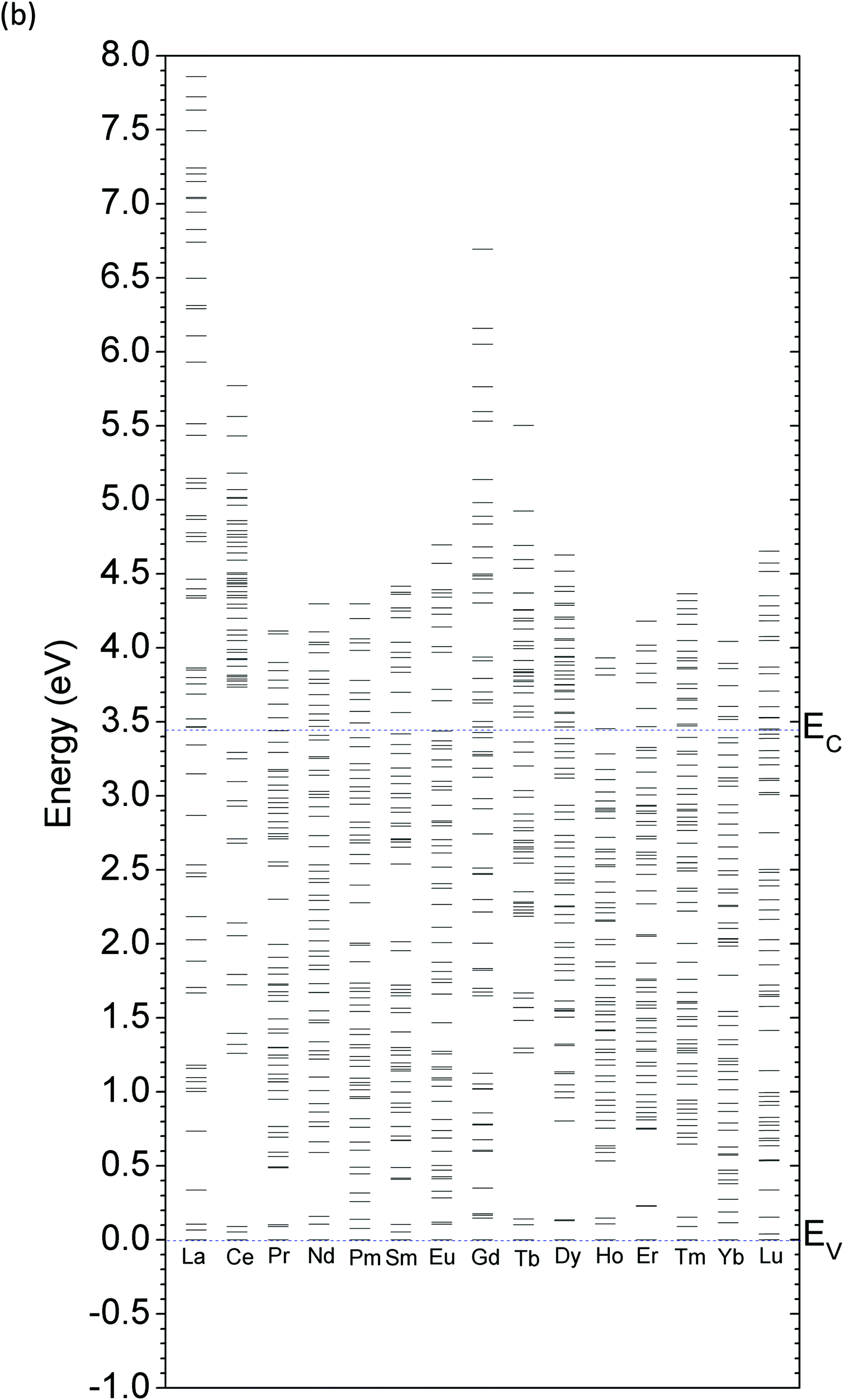
Thermodynamic transition levels of RE ions in the 2D ZnO system
The stability of the valence state of the doped RE ions in relation to the EF position within the band gap area is significant and can be determined by the TTLs, which is an important set of energy levels for measuring the zero-phonon line widths related to the CBM. As indicated in Fig. 11, most of the lanthanide elements in the REZn-doped systems provide rather shallow donor levels close to the CBM or within the CB range at the (0/+) transition. However, the transition level for the (+/2+) state is a deep donor level, which hardly provides the mobile electrons necessary to ionize electrons with large energy barriers into the CB (EC in Fig. 11). Most of the lanthanide substitutional dopants show positive Ueff features and can be detected on the surface of the sample using the ESR technique. | ||
| Fig. 11 Thermodynamic transition levels (TTL) of RE ions doped in the 2D-ZnO system by the charge state of 0, 1+, and 2+ for REZn (RE = La,…,Lu). | ||
The CeZn dopant is a relatively typical case in that its (+/2+) level is not as deep as that of other elements, while TbZn has a negative Ueff of −0.1 eV with a deep (0/2+) transition level. This behavior clearly shows that the TbZn dopant is not a donor source that provides freely mobile electrons in the ZnO lattice. EuZn doping also gives deep donor levels. As shown by the blue line in Fig. 11, the (0/+) and (+/2+) transition levels remain at EV +2.50 eV and EV +1.72 eV, respectively. These deep levels can only trap electrons at the EuZn site and may not ionize the electrons due to the large energy barrier below the CBM. Meanwhile, the single-particle calculation, shown in Fig. 9(b), indicates that Eu2+Zn may not be a red-emission center due to the 4f65d1–4f7 dipole transition, as the (0/+) level lies between the optical transitions and acts as an energy-depleting quench state.
More unusually, ErZn is found to be an extraordinary dopant with two contrasting (0/+) and (+/2+) TTLs. Er+ in the 2D ZnO system is stable and energetically favorable throughout the entire band gap area with variations in the EF. The (0/+) level is very shallow and aligns with the bottom of the CBM. Moreover, the TTL of the (+/2+) transition is found to be 0.76 eV below the VBM (or EV −0.76 eV, EV denotes the VBM), as shown in red in Fig. 11. As is known, the VB is the region in which bound valence electrons or delocalized energy transitions into free holes. This indicates that the (+/2+) transition produces free holes, and thus, Er2+ doped in the 2D ZnO system acts as a shallow acceptor center for capturing electrons or releasing free holes. This transition behavior may account for the experimentally reported enhanced NIR emission at 1540 nm induced by Er-doped ZnO nanomaterials.96,97
Excited states and relative oscillator strengths
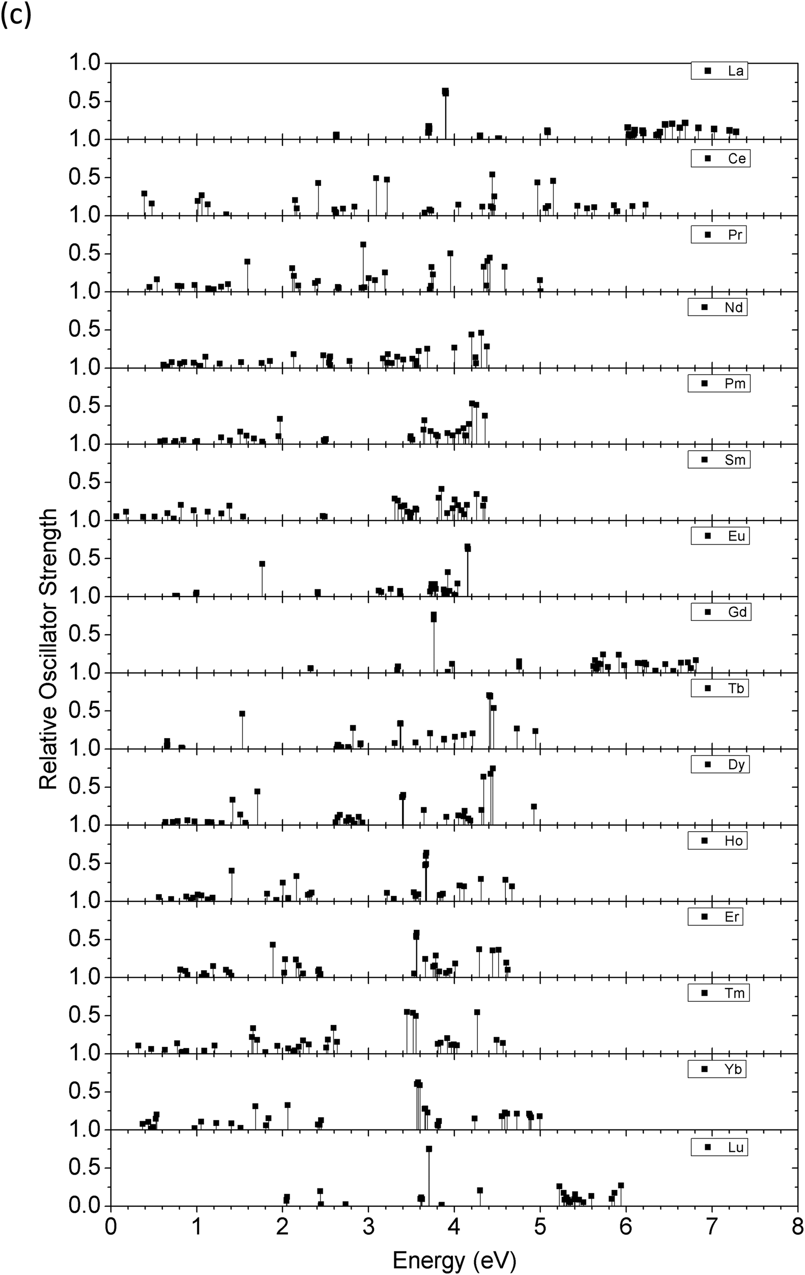
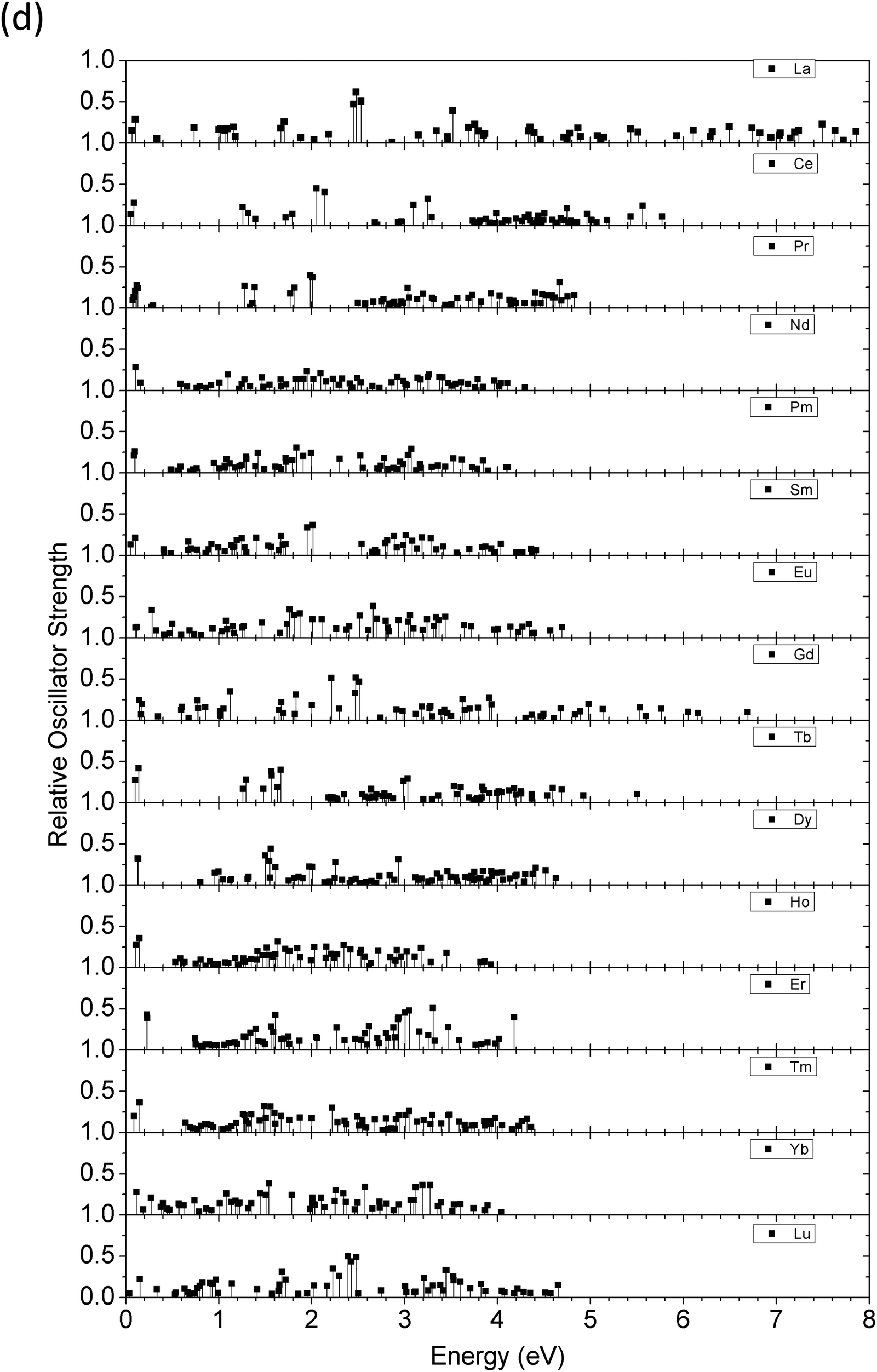
The excited states in ZnO doped with different divalent lanthanide ions (Ln2+, from La to Lu) were examined by a series of TD-DFT calculations, as shown in Fig. 12(a). These excitation energies correspond to the locations of the absorption peaks in the optical spectrum of a material and are more accurate than Kohn–Sham excitation energies. Some of the de-excitation paths between different energy levels correspond to the emission peaks from the output luminescence spectrum. The calculations were performed using the Tamm–Dankoff approximation.98 This method allows us to calculate the full set of optical properties with the support of the excitation energies and the corresponding transition probabilities. This study is also applicable to low-dimensional ZnO systems, as extra effects such as boundary effects, quantum-confinement effects, and different coordination-induced mixed-valence effects are necessarily taken into account.
 | ||
| Fig. 12 (a) Excited state levels for Ln2+ doping ions in ZnO. (b) Excited state levels for Ln3+ doping ions in ZnO. (c) The oscillator strength for each corresponding excited state of the Ln2+ doping ion. (d) The oscillator strength for each corresponding excited state of the Ln3+ doping ion. (e) The calculated oscillator strengths for Eu2+ and Eu3+ doping in ZnO are shown for comparison (G.S. denotes the ground state level located at 0 eV). | ||
Fig. 12(b) shows the excited state energy levels of trivalent lanthanide ions doped within the bulk ZnO host lattice. In contrast to the divalent ion-doped systems, the excited state energy levels are mostly distributed within the band gap area, especially in the lower energy range (<2.0 eV). This behavior indicates that Ln3+ ions have a much wider absorption window in the NIR excitation range than Ln2+ ions, as most of the Ln2+ excited state levels are near the CBM of the host ZnO with excitation energy near the band gap of ZnO (∼3.4 eV), as shown in Fig. 12(a).
Notably, Dorenbos et al. examined divalent and trivalent states of lanthanide elements doped in a crystal host (e.g., ZnO) and determined the minimum energy levels of the excited states.99–102 This examination of energy levels provides a significant starting point for further examination of energy transfer between different lanthanide ions, especially in the case of co-doping.
Meanwhile, it is helpful to consider the work-function or position relative to the vacuum level of a multi-faceted, low-dimensional ZnO nanomaterial system exposed to vacuum. This model is more realistic for the study of UC luminescence energy transfer in nanoparticles or nanocrystals. The calculations in this study are based on the bulk system, since the energy transfer mechanism and photoelectronic dynamics related to intrinsic defects or extrinsic dopants are still not very clear. Thus, we first examine the bulk system and then plan to extend our computational approach to other low-dimensional ZnO systems in the following studies.
Valence states of Ln ions doped in ZnO
We also considered Ln ions with mixed valences doped in ZnO. It is synthetically possible to produce mixed valence states of Ln ions between Ln2+ and Ln3+. These states may have different transition behaviors between excited state energy levels compared to the single-valence Ln2+ or Ln3+ ionic states. Here, we introduce that the excited state energy levels computed by TD-DFT together with the oscillator strength can be used to distinguish the different contributions to luminescence from the excited state energy level transitions. The relative oscillator strength determines the intensity of the absorption and emission by an external excitation source. Meanwhile, the relative oscillator strength illustrates the probability of transitions for the excited electrons and the kinetic rate constant for transitions among the different levels.Following the above discussion, we extracted the optical matrix elements from the calculations and converted them into relative oscillator strengths (transition probabilities) to discuss the probabilities of energy transfer as well as the lifetime of excited electrons at the specific level. The relative oscillator strength for each excited energy level is demonstrated in Fig. 12(c) and (d) for both Ln2+ and Ln3+ in the bulk ZnO lattice. In some cases, these excited state energy levels are dominated by contributions from the Russell–Saunders term 2S+1LJ, and the presentation of ladder-like energy levels is similar to the work of Dieke103 or Carnall et al.104 However, in most cases, the crystal-field splitting components, which contribute 4fN fine levels, are evident and rather dense in the energetic intervals,105 as shown in Fig. 12(a) and (b), which is in agreement with the work of Morrison et al.106 Here, in the wavefunctions, we account for all the effects of the energetic differences of the valence electrons with different behaviors. The physicochemical trend of the energy excitations of the electrons follows a similar trend as seen in the work of Carnall et al.104 Some deviations can be attributed to the bonding in ZnO, which is not a fully ionic crystal, such as LaF3, and contains partially covalent bonding features.
As shown in Fig. 12(e), Eu-doped ZnO can output red emission with a wavelength of approximately 650 nm (or 1.9 eV photon energy). In our calculated excited state, approximately 1.80 eV is necessary for the excited electron to de-excite back to the ground state. However, intermediate low energy states at approximately 1.0 eV may act as energy depletion paths to reduce the intensity of the emission, even though the oscillator strength is as small as 0.01. Meanwhile, as our thermodynamic transition levels illustrated, the deep transition levels of Eu-doped ZnO are unlikely to maintain the Eu2+ charge state in the energetic range of optical transitions near the midgap. Therefore, Eu2+Zn in the ZnO system may not be a highly efficient NIR/red luminescence center within the wavelength range of the first biological window. This corresponds to the experimental report that stated that the existence of Eu3+ in ZnO is actually responsible for the red luminescence.107,108 Meanwhile, the higher energy emission at 590 nm (2.1 eV), which was reported experimentally,35 that neighbors the Eu-intrinsic de-excitation at 615–650 nm is rather low and could be viewed as having zero oscillator strength, as shown in Fig. 12(e). Theoretically, both Eu2+ and Eu3+ can account for the observed red emission in ZnO, showing a similar trend as a recent experimental report.109 The probability analysis (oscillator strengths) of the divalent and trivalent states of Eu shows that two different energy transfer mechanisms can lead to red luminescence. Eu2+ shows two de-excitations from higher lying excited states back to the lower 5D0 level, followed by the second transition of 5D0 back to 7F0. For Eu3+, the electrons at two different excited states are de-excited back to the ground state, as shown in Fig. 12(e).
How can we further distinguish the real valence state of Eu ions doped in the ZnO system? Using TD-DFT calculations, we confirm that the transitions of Eu excitation levels in ZnO can be distinguished through differences in the luminescence intensity. According to the experimental observation by Hao et al.,35 longer wavelength emissions are always more intense in Eu-doped ZnO systems. As shown in Fig. 12(e), Eu2+ has a higher probability for energy transfer at larger energetic intervals. Thus, the divalent state of Eu does not act as the dominant red-emission center. Meanwhile, the mechanism for emission at 600 nm is unlikely to be the sole de-excitation from UC among the excited states. Indeed, red emission is supported by inter-defect-level transitions among the zero-phonon lines (with negative Ueff), leading to enhanced luminescence.51
Er doped in ZnO has been experimentally reported to generate NIR output luminescence at approximately 1540 nm (0.8 eV photon energy).110 In the Er2+ excited levels shown in Fig. 12(a), de-excitation from the first excited state back to the ground state (0 eV) may correspond to the luminescence energetic output with an interval of 0.81 eV (1530 nm wavelength). For the Er3+ excited states, the output may result from a transition from the second excited state back to the first excited state with an interval of 0.52 eV, which is slightly larger than the Er2+ emission wavelength. However, in the medium energetic scale, Er-doped ZnO outputs green emission, showing twin peaks from 525 nm to 560 nm.110 As shown in Fig. 12(a) and (b), Er2+ and Er3+ both contribute to energy transitions, with Er3+ showing a slightly higher oscillator strength. Therefore, luminescence in ZnO due to Er doping probably has a mixed valence state between 2+ and 3+ or potentially exhibits a valence state transition resulting from different external excitations, such as different injection currents or voltages via the electroluminescence (EL) technique.110
Er doping in wide-band-gap, group III–V semiconductors has been studied at low temperature, and emission at 1540 nm has been reported to result from transitions from the first excited spin–orbit state 4I13/2 to the 4I15/2 ground state of Er3+ (4f11). However, so far, there is no conclusive evidence of the lattice site of luminescent Er ions in a specific valence state.111 The (Er,Tm) co-doping of ZnO has also shown that emission at 1540 nm can be observed by Er and Tm individually, which indicates that the energy scale allows for intrinsic transitions of Tm ions doped in the ZnO lattice.112 As seen in Fig. 12(c) and (d), Tm2+ ions lead to very small energy splitting between the spin–orbit transition from 3F4 to 3H6, while Tm3+ ions undergo a transition with similar energy and a relatively high oscillator strength. For emission in the shorter wavelength range, the Tm-doped ZnO thin film can achieve the observed blue (480 nm) and red (800 nm) emissions via the electroluminescence (EL) technique, using a higher injection current and voltage.110 As shown in Fig. 12(c), there are two distinctly high oscillator strengths below 3.0 eV at approximately 1.61 eV and 2.60 eV. Therefore, Tm3+ in ZnO is responsible for the long-wavelength NIR emissions at 1540 nm and 1800 nm,112 while Tm2+ in ZnO can account for the emissions at 480 nm and 800 nm generated by the electroluminescence (EL) technique.110
Energy transport and modulation
We summarized the oscillator strength and the corresponding excited state energy levels of all 15 lanthanide ions in the 2+ and 3+ charge states, as shown in Fig. 13(a) and (b), respectively. In the Ln2+ doping state (Fig. 13(a)), energy transitions at the CBM edge absorption or higher (∼3.4 eV or >3.4 eV) predominate medium and heavy lanthanide ions. The light lanthanide elements have excited state energy transition levels within the band gap with lower oscillator strength compared to the medium or heavy lanthanides.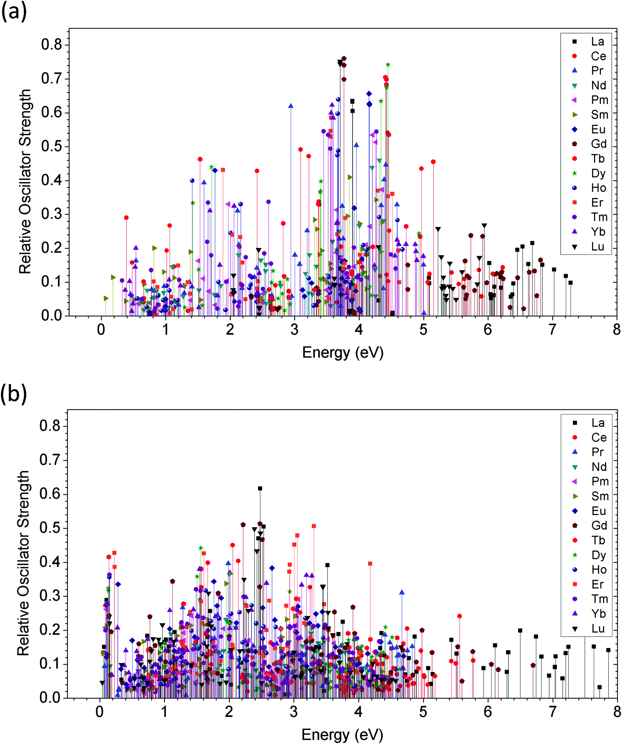

 | ||
| Fig. 13 (a) The relative oscillator strength for each corresponding excited state is shown by the 15 lanthanide doping ions within the bulk ZnO lattice. The levels of divalent ions and trivalent ions are shown in (a) and (b), respectively. The summary of the relationship between oscillator strength and excited state energy level is shown in 3-dimensions (3D) with Ln2+ (c) and Ln3+ (d). The Smith-charts illustrate a range of 15 lanthanide dopant ions in ZnO for modulating the output emission luminescence properties, where the Ln2+ ions are shown in (e) and Ln3+ are shown in (f). | ||
However, the situation is clearly different for the Ln3+ doping state (Fig. 13(b)). The oscillator strengths of all lanthanide ions are reduced, and the excited state energy levels are shifted to below 3.0 eV. This phenomenon is very similar to a famous concept in biology called the removal of apical dominance. This concept is usually observed in living plants, in which the apex of the plant has a rather strong tendency to grow, resulting in inhibited development of the lower branches. This originates from unbalanced plant food absorption, which is stronger at the top apex than in the branches. Continuous energy harvesting induces transportation paths for growth auxins (or phytohormones), which is the main cause of inhibition. Manually removing the apex will stop energy transport to the top and shift it to the lower branches so that the living plant can achieve wider plant growth. Analogous to energy transport and conversion in Ln-doped UCNPs, Ln3+ ions, as the sensitizing dopant, reduce the energy barrier for excited state absorption, showing wider energy transfer channels that are evenly distributed within 3.0 eV, which is lower than the CB edge absorption in Ln2+-doped ZnO. Meanwhile, each energy level has a stronger oscillator strength, indicating a larger probability for excitation and energy transport between the inter-levels. This phenomenon for trivalent Ln doping, in physicochemical and biological terms, follows the removal of apical dominance concept, leading to more flexible energy transfer within the biological window.
Further details are shown in Fig. 13(c) and (d) in a 3D view. The higher energy transitions from Ln2+ to Ln3+ are not suppressed by forbidden transitions or real quenching effects induced by different trap levels. Instead, the inhibition results from competition among the various kinetic reaction rate constants of the lanthanide dopant ions. Yan et al. provided a similar discussion of the rate constant competition and transfer by studying the UC luminescence of a NaYF4@CaF2(Er,Yb) core@shell system.113,114
Finally, to design an optimal transmission channel for energy transfer among sensitizer and activator ions, as well as energy transport through the lattice, the oscillator strength and excited state energy levels must be comprehensively considered. Proper transfer and transport require not only a large probability (oscillator strength) of transition between excited state levels but also a wide and even distribution of these levels that largely overlaps with the intrinsic band structure of the host. Meanwhile, the conventional view of 4f-dominated transitions among excited states is no longer universally accepted to interpret different energy transfers of UC luminescence, which may restrict the future synthesis of novel nanoparticles with easily modulated output luminescence. Actually, d–f hybrid transitions of the lanthanide doping ions within various systems can contribute different charge-transfer-induced energy migrations between the excited states of different ions,115 which is potentially useful to support energy transfer for self-sensitization, such as that for a rather wide-band-gap host lattice at 654 nm (1.89 eV photon energy).116
To establish a correlation between the excited energy levels and the corresponding oscillator strengths, we summarized these parameters in a Smith chart to understand the overarching relationships. The horizontal direction gives the excited energy levels, while the vertical direction shows the oscillator strength. We approximated the lifetime and cross-relaxation into a phase difference via an exponential decay function to give an overall graphical view of the potential high-efficiency energy transfer in UC luminescence materials composed of lanthanide-doped ZnO.
In addition, the Smith chart in Fig. 13(e) illustrates that heavy lanthanide elements usually dominate the energy transmission channel at high energy, medium lanthanide elements mostly occupy the middle range of the optical fundamental gap, and light lanthanide elements are widely spread over the optical band gap, as well as over the partial CB range.
However, as shown in Fig. 13(f), following the removal of apical dominance concept, Ln3+ shows wider distributed energy transfer channels within 3.0 eV, contributing a more flexible biological window for in vivo imaging or other related optoelectronic devices.
Lifetime and decay time
The emission time for luminescence materials can be divided into two ranges depending on the length and mechanism: fluorescence and phosphorescence. Persistent luminescence is an optical phenomenon attributed to phosphorescence persisting for several seconds to hours or even days.The lifetime τ is an important parameter for describing the fluorescence resulting from inter-level transitions between excited states. For emission, τ ∝ 1/(ω3D2), where ω is the photon frequency (i.e., photon energy is ℏω) and D is the dipole moment. In another description following the Lorentz local field under the vacuum cavity model framework, the lifetime is correlated to the oscillator strength: τ ∼ (1/f)[9nλ0(n2 + 2)2], where f is approximated by the electric-dipole transition, λ0 is the emission wavelength and n is the refraction index of the luminescence sample.117
However, the situation is different for persistent luminescence (phosphorescence). The lifetime τ for the fluorescent is no longer effectively described the persistent luminescence. As Leverenz summarized,118,119 excited electrons are trapped by intrinsic defects or extrinsic impurities in the host, and most of these trap depths are evidently distant from the delocalized states near the CB edge. Therefore, the luminescence time is described by the exponential decay function I = I0![[thin space (1/6-em)]](https://www.rsc.org/images/entities/char_2009.gif) exp(−at), which is independent of the luminescence temperature, via the power law I = I0t−n, but dependent on the phosphor temperature. Our recent work was consistent with the Leverenz model in that energy transfer in persistent luminescence is likely independent of the temperature but is strongly correlated with electron-lattice coupling in the defect states.51 Currently, no universal analytic theoretical equations for the decay time exist; however, the decay time can be expressed by an effective multi-center emission approximation with consideration of the thermal effects as follows:
exp(−at), which is independent of the luminescence temperature, via the power law I = I0t−n, but dependent on the phosphor temperature. Our recent work was consistent with the Leverenz model in that energy transfer in persistent luminescence is likely independent of the temperature but is strongly correlated with electron-lattice coupling in the defect states.51 Currently, no universal analytic theoretical equations for the decay time exist; however, the decay time can be expressed by an effective multi-center emission approximation with consideration of the thermal effects as follows:
| I(t) = I01exp[−v1texp(−ΔE1/kBT)] + I02exp[−v2texp(−ΔE2/kBT)] + ⋯ + I0Nexp[−vNtexp(−ΔEN/kBT)], | (2) |
In this work, as shown in Fig. 8–10, the calculated single-particle levels determine the trap depth of each lanthanide dopant, which describes its contribution to the persistent luminescence of ZnO. Meanwhile, these localized electron and hole states also reduce the energy barrier for bound electrons to transfer from the VBM to the CBM directly from the host lattice. If we choose a lanthanide element as the first dopant to act as a luminescence center (i.e., activator), then a suitable secondary dopant must be determined to extend the lifetime.
As shown in Fig. 8, among the light lanthanide elements, Ce and Pr are suitable candidates for extending the persistent luminescence lifetime (or decay time) because Ce and Pr have relatively low electron trap levels, which are low-lying in the optical band gap. As noted in eqn (2), the deeper the trap depth, the longer the decay time of persistent luminescence. Among the medium lanthanide elements, as shown in Fig. 9, Eu, Tb, and Dy are suitable secondary dopants to prolong the decay time via extending the trap depth to even deeper positions, particularly the dopant Dy. Previous studies have confirmed that Dy is a suitable secondary dopant for the temporal extension of persistent luminescence.84,120,121 Among the heavy lanthanide elements, as shown in Fig. 10, no suitable candidates provide electronic trap levels far enough away from the CBM. Thus, among all the lanthanide elements, Dy is the best secondary dopant for the persistent luminescence of ZnO nanomaterials. Note that this deduction is only valid based on the trap-depth model by Leverenz. Further theoretical analysis of the decay time of persistent luminescence will be explored in future work.
Summary
The doping limits in various ZnO structures were determined by their native point defect formation energies. Chemical trends of the doping limits of ZnO were shown by comparing the formation energy and the EF in terms of doping pinning limit energies. Furthermore, the doping limits and corrected electronic properties were examined for an amorphous solid ZnO material. We found that the am-ZnO system is p-type dopable with acceptor dopants, since its p-type pinning energy overlaps with the VB edge. However, p-type doping is achieved at the cost of lower electronic affinities of various Zn- or O-sites, indicating a potential loss of the n-type behavior of ZnO. The 2D ZnO system expands the doping limit range from the VB to the CB edge, indicating that 2D ZnO is a promising low-dimensional nanomaterial. This material not only lowers the coordinate numbers of the Zn and O sites, which lowers the electron affinity, but also shifts the charge neutrality level towards the lower part of the band gap close to the VB edge.To further our examination of energy transfer in UC luminescence by RE ion doping, the excited state levels were extensively studied for all 15 lanthanide (Ln) elements in both the Ln2+ and Ln3+ ionic charge state. We also considered the probability of mixed valences of the Ln dopant ions occurring in ZnO and analyzed the relative oscillator strengths to discuss the transition probabilities for energy transfer by excited electrons at the specific level. We found that at the Ln2+ charge state, heavy lanthanide elements usually dominate the energy transmission channel at high energy, medium lanthanide elements mostly occupy the middle range of the optical fundamental gap, and light lanthanide elements are widely spread over the optical band gap as well as over the partial CB range. However, at the Ln3+ charge state, following the removal of apical dominance concept, Ln3+ has wider distributed energy transfer channels within 3.0 eV, which contributes a more flexible biological window for in vivo imaging or other related optoelectronic devices.
Acknowledgements
This work is supported by the Natural Science Foundation of China (NSFC) for the Young Scientist grant (Grant No. NSFC 11504309), the initial start-up grant support from the Department General Research Fund (Dept. GRF) from ABCT at Hong Kong Polytechnic University, and the Early Career Scheme (ECS) Fund (Grant No. PolyU 253026/16P) from the Research Grant Council (RGC) in Hong Kong.References
- Ü. Özgür, Y. I. Alivov, C. Liu, A. Teke, M. A. Reshchikov, S. Doğan, V. Avrutin, S.-J. Cho and H. Morkoç, J. Appl. Phys., 2005, 98, 041301 CrossRef.
- K. Hiruma, M. Yazawa, T. Katsuyama, K. Ogawa, K. Haraguchi, M. Koguchi and H. Kakibayashi, J. Appl. Phys., 1995, 77, 447 CrossRef CAS.
- J. Hu, T. W. Odom and C. M. Lieber, Acc. Chem. Res., 1999, 32, 435 CrossRef CAS.
- Z. W. Pan, Z. R. Dai and Z. L. Wang, Science, 2001, 291, 1947 CrossRef CAS PubMed.
- M. H. Huang, S. Mao, H. Feick, H. Yan, Y. Wu, H. Kind, E. Weber, R. Russo and P. Yang, Science, 2001, 292, 1897 CrossRef CAS PubMed.
- M. Law, L. E. Greene, J. C. Johnson, R. Saykally and P. Yang, Nat. Mater., 2005, 4, 455 CrossRef CAS PubMed.
- J. J. Cole, X. Wang, R. J. Knuesel and H. O. Jacobs, Nano Lett., 2008, 8, 1477 CrossRef CAS PubMed.
- H. Cao, J. Y. Xu, D. Z. Zhang, S. H. Chang, S. T. Ho, E. W. Seelig, X. Liu and R. P. H. Chang, Phys. Rev. Lett., 2000, 84, 5584 CrossRef CAS PubMed.
- H. Cao, J. Y. Xu, E. W. Seelig and R. P. H. Chang, Appl. Phys. Lett., 2000, 76, 2997 CrossRef CAS.
- H.-M. Xiong, Adv. Mater., 2013, 25, 5329 CrossRef CAS PubMed.
- C. Zhang, F. Zhang, T. Xia, N. Kumar, J.-i. Hahm, J. Liu, Z. L. Wang and J. Xu, Opt. Express, 2009, 17, 7893 CrossRef CAS PubMed.
- J. E. Stehr, S. L. Chen, N. K. Reddy, C. W. Tu, W. M. Chen and I. A. Buyanova, Adv. Funct. Mater., 2014, 24, 3760 CrossRef CAS.
- F. Auzel, Chem. Rev., 2004, 104, 139 CrossRef CAS PubMed.
- F. van de Rijke, H. Zijlmans, S. Li, T. Vail, A. K. Raap, R. S. Niedbala and H. J. Tanke, Nat. Biotechnol., 2001, 19, 273 CrossRef CAS PubMed.
- S. F. Lim, R. Riehn, W. S. Ryu, N. Khanarian, C.-k. Tung, D. Tank and R. H. Austin, Nano Lett., 2006, 6, 169 CrossRef CAS PubMed.
- M. Nyk, R. Kumar, T. Y. Ohulchanskyy, E. J. Bergey and P. N. Prasad, Nano Lett., 2008, 8, 3834 CrossRef CAS PubMed.
- B. E. Cohen, Nature, 2010, 467, 407 CrossRef CAS PubMed.
- F. Wang, et al. , Nature, 2010, 463, 1061 CrossRef CAS PubMed.
- D. A. Parthenopoulos and P. M. Rentzepis, Science, 1989, 245, 843 CAS.
- E. Downing, L. Hesselink, J. Ralston and R. Macfarlane, Science, 1996, 273, 1185 CAS.
- F. Wang, R. Deng, J. Wang, Q. Wang, Y. Han, H. Zhu, X. Chen and X. Liu, Nat. Mater., 2011, 10, 968 CrossRef CAS PubMed.
- A. M. Ibarra-Ruiz, D. C. Rodríguez Burbano and J. A. Capobianco, Advances in Physics: X, 2016, 1, 194 CrossRef.
- S. Gai, C. Li, P. Yang and J. Lin, Chem. Rev., 2014, 114, 2343 CrossRef CAS PubMed.
- N. M. Idris, M. K. G. Jayakumar, A. Bansal and Y. Zhang, Chem. Soc. Rev., 2015, 44, 1449 RSC.
- T. Saeed and P. O'Brien, Thin Solid Films, 1995, 271, 35 CrossRef CAS.
- L. E. Greene, M. Law, J. Goldberger, F. Kim, J. C. Johnson, Y. Zhang, R. J. Saykally and P. Yang, Angew. Chem., Int. Ed., 2003, 42, 3031 CrossRef CAS PubMed.
- M. Kokotov, A. Biller and G. Hodes, Chem. Mater., 2008, 20, 4542 CrossRef CAS.
- R. R. Gadde and H. A. Laitinen, Anal. Chem., 1974, 46, 2022 CrossRef CAS.
- J. Zhang, L. Sun, H. Pan, C. Liao and C. Yan, New J. Chem., 2002, 26, 33 RSC.
- J. Zhang, L. Sun, C. Liao and C. Yan, Chem. Commun., 2002, 262 RSC.
- J. Zhang, L. Sun, J. Yin, H. Su, C. Liao and C. Yan, Chem. Mater., 2002, 14, 4172 CrossRef CAS.
- J. Zhang, L.-D. Sun, X.-C. Jiang, C.-S. Liao and C.-H. Yan, Cryst. Growth Des., 2004, 4, 309 CAS.
- D.-F. Zhang, L.-D. Sun, J.-L. Yin, C.-H. Yan and R.-M. Wang, J. Phys. Chem. B, 2005, 109, 8786 CrossRef CAS PubMed.
- D.-F. Zhang, L.-D. Sun, J. Zhang, Z.-G. Yan and C.-H. Yan, Cryst. Growth Des., 2008, 8, 3609 CAS.
- D. Yue, W. Lu, L. Jin, C. Li, W. Luo, M. Wang, Z. Wang and J. Hao, Nanoscale, 2014, 6, 13795 RSC.
- Z.-P. Zhang, et al. , Nanoscale, 2016, 8, 15744 RSC.
- S. B. Zhang, S.-H. Wei and A. Zunger, J. Appl. Phys., 1998, 83, 3192 CrossRef CAS.
- S. B. Zhang, S. H. Wei and A. Zunger, Phys. Rev. B: Condens. Matter Mater. Phys., 2001, 63, 075205 CrossRef.
- J. Robertson and S. J. Clark, Phys. Rev. B: Condens. Matter Mater. Phys., 2011, 83, 075205 CrossRef.
- S. J. Clark, J. Robertson, S. Lany and A. Zunger, Phys. Rev. B: Condens. Matter Mater. Phys., 2010, 81, 115311 CrossRef.
- A. F. Kohan, G. Ceder, D. Morgan and C. G. Van de Walle, Phys. Rev. B: Condens. Matter Mater. Phys., 2000, 61, 15019 CrossRef CAS.
- A. Janotti and C. G. Van de Walle, Phys. Rev. B: Condens. Matter Mater. Phys., 2007, 76, 165202 CrossRef.
- C. G. Van de Walle, Phys. Rev. Lett., 2000, 85, 1012 CrossRef CAS PubMed.
- A. Janotti and C. G. Van de Walle, Nat. Mater., 2007, 6, 44 CrossRef CAS PubMed.
- S. J. Clark and J. Robertson, Phys. Rev. B: Condens. Matter Mater. Phys., 2010, 82, 085208 CrossRef.
- J. M. Khoshman and M. E. Kordesch, Thin Solid Films, 2007, 515, 7393 CrossRef CAS.
- S. Lany and A. Zunger, Phys. Rev. Lett., 2004, 93, 156404 CrossRef PubMed.
- S. Lany and A. Zunger, Phys. Rev. B: Condens. Matter Mater. Phys., 2005, 72, 035215 CrossRef.
- B. Huang, Phys. Chem. Chem. Phys., 2016, 18, 13564 RSC.
- B. Huang, Phys. Chem. Chem. Phys., 2016, 18, 25946 RSC.
- B. Huang and M. Sun, Phys. Chem. Chem. Phys., 2017, 19, 9457 RSC.
- D. V. Lang and R. A. Logan, Phys. Rev. Lett., 1977, 39, 635 CrossRef CAS.
- R. M. Rubinger, J. C. Bezerra, E. F. Chagas, J. C. González, W. N. Rodrigues, G. M. Ribeiro, M. V. B. Moreira and A. G. de Oliveira, J. Appl. Phys., 1998, 84, 3764 CrossRef CAS.
- E. R. Viana, J. C. González, G. M. Ribeiro and A. G. de Oliveira, J. Phys. Chem. C, 2013, 117, 7844 CAS.
- H. J. Queisser and D. E. Theodorou, Phys. Rev. B: Condens. Matter Mater. Phys., 1986, 33, 4027 CrossRef CAS.
- H. J. Queisser, Phys. Rev. Lett., 1985, 54, 234 CrossRef CAS PubMed.
- J. Clark Stewart, D. Segall Matthew, J. Pickard Chris, J. Hasnip Phil, I. J. Probert Matt, K. Refson and C. Payne Mike, Z. Kristallogr., 2005, vol. 220, p. 567 Search PubMed.
- L. Kleinman and D. M. Bylander, Phys. Rev. Lett., 1982, 48, 1425 CrossRef CAS.
- S. G. Louie, S. Froyen and M. L. Cohen, Phys. Rev. B: Condens. Matter Mater. Phys., 1982, 26, 1738 CrossRef CAS.
- I. Grinberg, N. J. Ramer and A. M. Rappe, Phys. Rev. B: Condens. Matter Mater. Phys., 2000, 62, 2311 CrossRef CAS.
- A. M. Rappe, K. M. Rabe, E. Kaxiras and J. D. Joannopoulos, Phys. Rev. B: Condens. Matter Mater. Phys., 1990, 41, 1227 CrossRef.
- N. Marzari, D. Vanderbilt and M. C. Payne, Phys. Rev. Lett., 1997, 79, 1337 CrossRef CAS.
- B. Huang, R. Gillen and J. Robertson, J. Phys. Chem. C, 2014, 118, 24248 CAS.
- M. I. J. Probert and M. C. Payne, Phys. Rev. B: Condens. Matter Mater. Phys., 2003, 67, 075204 CrossRef.
- I. A. Vladimir, F. Aryasetiawan and A. I. Lichtenstein, J. Phys.: Condens. Matter, 1997, 9, 767 CrossRef.
- S. Lany and A. Zunger, Phys. Rev. B: Condens. Matter Mater. Phys., 2009, 80, 085202 CrossRef.
- S. Lany and A. Zunger, Phys. Rev. B: Condens. Matter Mater. Phys., 2010, 81, 205209 CrossRef.
- B. J. Morgan and G. W. Watson, J. Phys. Chem. C, 2010, 114, 2321 CAS.
- P. R. L. Keating, D. O. Scanlon, B. J. Morgan, N. M. Galea and G. W. Watson, J. Phys. Chem. C, 2011, 116, 2443 Search PubMed.
- B. Huang, Philos. Mag., 2014, 94, 3052 CrossRef CAS.
- B. Huang, J. Comput. Chem., 2016, 37, 825 CrossRef CAS PubMed.
- B. Huang, Phys. Chem. Chem. Phys., 2017, 19, 8008 RSC.
- S. Lany and A. Zunger, Phys. Rev. B: Condens. Matter Mater. Phys., 2008, 78, 235104 CrossRef.
- D. B. Laks, C. G. Van de Walle, G. F. Neumark, P. E. Blöchl and S. T. Pantelides, Phys. Rev. B: Condens. Matter Mater. Phys., 1992, 45, 10965 CrossRef CAS.
- S.-H. Wei, Comput. Mater. Sci., 2004, 30, 337 CrossRef CAS.
- G. Makov and M. C. Payne, Phys. Rev. B: Condens. Matter Mater. Phys., 1995, 51, 4014 CrossRef CAS.
- B. Huang, Solid State Commun., 2016, 237–238, 34 CrossRef CAS.
- F. Oba, A. Togo, I. Tanaka, J. Paier and G. Kresse, Phys. Rev. B: Condens. Matter Mater. Phys., 2008, 77, 245202 CrossRef.
- B. Huang, Solid State Commun., 2016, 230, 49 CrossRef CAS.
- F. Tuomisto, V. Ranki, K. Saarinen and D. C. Look, Phys. Rev. Lett., 2003, 91, 205502 CrossRef CAS PubMed.
- D. C. Look, J. W. Hemsky and J. R. Sizelove, Phys. Rev. Lett., 1999, 82, 2552 CrossRef CAS.
- J. Anderson and G. V. d. W. Chris, Rep. Prog. Phys., 2009, 72, 126501 CrossRef.
- S. Lany and A. Zunger, Phys. Rev. B: Condens. Matter Mater. Phys., 2010, 81, 113201 CrossRef.
- B. Huang, Inorg. Chem., 2015, 54, 11423 CrossRef CAS PubMed.
- B. Parthapratim, D. N. Tafen, F. Inam, C. Bin and D. A. Drabold, J. Phys.: Condens. Matter, 2009, 21, 084207 CrossRef PubMed.
- A. Roy, Y.-T. Cheng and M. L. Falk, J. Phys. Chem. C, 2016, 120, 2529 CAS.
- M. Dutta, S. Sarkar, T. Ghosh and D. Basak, J. Phys. Chem. C, 2012, 116, 20127 CAS.
- J. O. Hwang, D. H. Lee, J. Y. Kim, T. H. Han, B. H. Kim, M. Park, K. No and S. O. Kim, J. Mater. Chem., 2011, 21, 3432 RSC.
- Y. Y. Hui, G. a. Tai, Z. Sun, Z. Xu, N. Wang, F. Yan and S. P. Lau, Nanoscale, 2012, 4, 3118 RSC.
- Q. Yao, Y. Liu, R. Lu, C. Xiao, K. Deng and E. Kan, RSC Adv., 2014, 4, 17478 RSC.
- W. Hu, Z. Li and J. Yang, J. Chem. Phys., 2013, 138, 124706 CrossRef PubMed.
- W. Geng, X. Zhao, H. Liu and X. Yao, J. Phys. Chem. C, 2013, 117, 10536 CAS.
- W. Geng, X. Zhao, W. Zan, H. Liu and X. Yao, Phys. Chem. Chem. Phys., 2014, 16, 3542 RSC.
- S. Lany and A. Zunger, Phys. Rev. B: Condens. Matter Mater. Phys., 2009, 80, 085202 CrossRef.
- S. Lany and A. Zunger, Phys. Rev. B: Condens. Matter Mater. Phys., 2010, 81, 205209 CrossRef.
- F. Xiao, R. Chen, Y. Q. Shen, Z. L. Dong, H. H. Wang, Q. Y. Zhang and H. D. Sun, J. Phys. Chem. C, 2012, 116, 13458 CAS.
- J.-W. Lo, W.-C. Lien, C.-A. Lin and J.-H. He, ACS Appl. Mater. Interfaces, 2011, 3, 1009 CAS.
- S. Hirata and M. Head-Gordon, Chem. Phys. Lett., 1999, 314, 291 CrossRef CAS.
- P. Dorenbos, J. Lumin., 2004, 108, 301 CrossRef CAS.
- P. Dorenbos, Chem. Mater., 2005, 17, 6452 CrossRef CAS.
- P. Dorenbos, Phys. Rev. B: Condens. Matter Mater. Phys., 2012, 85, 165107 CrossRef.
- P. Dorenbos and E. van der Kolk, SPIE Proc., 2007, 647313 CrossRef.
- G. H. Dieke, H. M. Crosswhite and H. Crosswhite, Spectra and energy levels of rare earth ions in crystals, Interscience Publishers, New York, 1968 Search PubMed.
- W. T. Carnall, G. L. Goodman, K. Rajnak and R. S. Rana, J. Chem. Phys., 1989, 90, 3443 CrossRef CAS.
- P. Tanner, in Lanthanide Luminescence, ed. P. Hänninen and H. Härmä, Springer Berlin Heidelberg, 2011, vol. 7, p. 183 Search PubMed.
- C. A. Morrison and R. P. Leavitt, J. Chem. Phys., 1979, 71, 2366 CrossRef CAS.
- D. Wang, G. Xing, M. Gao, L. Yang, J. Yang and T. Wu, J. Phys. Chem. C, 2011, 115, 22729 CAS.
- Q. Yu, T. Ai, L. Jiang, Y. Zhang, C. Li and X. Yuan, RSC Adv., 2014, 4, 53946 RSC.
- H. Akazawa and H. Shinojima, J. Appl. Phys., 2016, 120, 123101 CrossRef.
- Y. Yang, Y. Li, C. Wang, C. Zhu, C. Lv, X. Ma and D. Yang, Adv. Opt. Mater., 2014, 2, 240 CrossRef.
- H. Ennen, J. Schneider, G. Pomrenke and A. Axmann, Appl. Phys. Lett., 1983, 43, 943 CrossRef CAS.
- Y. Pu, F. Xu, Z. Jiang, Z. Ma, F. Lu and D. Chen, Appl. Phys. Lett., 2012, 101, 191903 CrossRef.
- Y.-F. Wang, L.-D. Sun, J.-W. Xiao, W. Feng, J.-C. Zhou, J. Shen and C.-H. Yan, Chem. – Eur. J., 2012, 18, 5558 CrossRef CAS PubMed.
- H. Dong, L.-D. Sun and C.-H. Yan, Chem. Soc. Rev., 2015, 44, 1608 RSC.
- S. J. A. Pope, B. J. Coe, S. Faulkner, E. V. Bichenkova, X. Yu and K. T. Douglas, J. Am. Chem. Soc., 2004, 126, 9490 CrossRef CAS PubMed.
- Q. Chen, X. Xie, B. Huang, L. Liang, S. Han, Z. Yi, Y. Wang, Y. Li, D. Fan, L. Huang and X. Liu, Angew. Chem., Int. Ed., 2017 DOI:10.1002/anie.201703012R1.
- Y. Liu, W. Luo, R. Li, G. Liu, M. R. Antonio and X. Chen, J. Phys. Chem. C, 2008, 112, 686 CAS.
- H. W. Leverenz, Science, 1949, 109, 183 CAS.
- H. W. Leverenz, Science, 1967, 157, 414 Search PubMed.
- D. C. Rodriguez Burbano, E. M. Rodriguez, P. Dorenbos, M. Bettinelli and J. A. Capobianco, J. Mater. Chem. C, 2014, 2, 228 RSC.
- D. C. Rodríguez Burbano, S. K. Sharma, P. Dorenbos, B. Viana and J. A. Capobianco, Adv. Opt. Mater., 2015, 3, 551 CrossRef.
| This journal is © the Owner Societies 2017 |