
 Open Access Article
 This Open Access Article is licensed under a
 Creative Commons Attribution 3.0 Unported Licence
Erbium ion implantation into diamond – measurement and modelling of the crystal structure†
Jakub
Cajzl
*ab,
Pavla
Nekvindová
a,
Anna
Macková
cd,
Petr
Malinský
cd,
David
Sedmidubský
a,
Michal
Hušák
a,
Zdeněk
Remeš
e,
Marián
Varga
e,
Alexander
Kromka
e,
Roman
Böttger
f and
Jiří
Oswald
e
aDepartment of Inorganic Chemistry, University of Chemistry and Technology, Technická 5, 166 28 Prague, Czech Republic. E-mail: cajzlj@vscht.cz
bInstitute of Photonics and Electronics, Czech Academy of Sciences, v.v.i., Chaberská 57, 182 51 Prague, Czech Republic
cNuclear Physics Institute, Czech Academy of Sciences, v.v.i., 250 68 Řež, Czech Republic
dDepartment of Physics, J.E. Purkinje University, České mládeže 8, 400 96 Ústí nad Labem, Czech Republic
eInstitute of Physics, Czech Academy of Sciences, v.v.i., Cukrovarnická 10/112, 162 00 Prague, Czech Republic
fHelmholtz-Zentrum Dresden-Rossendorf, Institute of Ion Beam Physics and Materials Research, Bautzner Landstraße 400, 01328 Dresden, Germany
First published on 26th January 2017
Abstract
Diamond is proposed as an extraordinary material usable in interdisciplinary fields, especially in optics and photonics. In this contribution we focus on the doping of diamond with erbium as an optically active centre. In the theoretical part of the study based on DFT simulations we have developed two Er-doped diamond structural models with 0 to 4 carbon vacancies in the vicinity of the Er atom and performed geometry optimizations by the calculation of cohesive energies and defect formation energies. The theoretical results showed an excellent agreement between the calculated and experimental cohesive energies for the parent diamond. The highest values of cohesive energies and the lowest values of defect formation energies were obtained for models with erbium in the substitutional carbon position with 1 or 3 vacancies in the vicinity of the erbium atom. From the geometry optimization the structural model with 1 vacancy had an octahedral symmetry whereas the model with 3 vacancies had a coordination of 10 forming a trigonal structure with a hexagonal ring. In the experimental part, erbium doped diamond crystal samples were prepared by ion implantation of Er+ ions using ion implantation fluences ranging from 1 × 10¹⁴ ions per cm2 to 5 × 10¹⁵ ions per cm2. The experimental results revealed a high degree of diamond structural damage after the ion implantation process reaching up to 69% of disordered atoms in the samples. The prepared Er-doped diamond samples annealed at the temperatures of 400, 600 and 800 °C in a vacuum revealed clear luminescence, where the 〈110〉 cut sample has approximately 6–7 times higher luminescence intensity than the 〈001〉 cut sample with the same ion implantation fluence. The reported results are the first demonstration of the Er luminescence in the single crystal diamond structure for the near-infrared spectral region.
1. Introduction
Diamond exhibits outstanding physical and chemical properties such as extremely high chemical and thermal resistance, and the highest hardness and thermal conductivity among all materials. Moreover, diamond is also biocompatible due to its carbon nature.1 Thanks to these properties, diamond is intensively studied for use in electronics, photonics and integrated quantum photonics. In electronics, diamond is mostly studied for its use as p- and n-type semiconductors. For these purposes, it has been doped with various dopants to create a p-type diamond (doping with boron2,3) or n-type diamond (doping with nitrogen, phosphorus or sulphur4).In the photonics field, micro- or nanocrystalline diamond (MCD or NCD) thin films grown on silicon or SiO2 have been used for special High Index Contrast (HIC) waveguides.5 The estimated relative refractive index difference Δn reaches a high value of about 30% for the glass/NCD. This high value of refractive index difference makes diamond HIC waveguides suitable for photonic waveguiding structures with a high density of integration.6,7 However, the high degree of optical attenuation mainly due to the scattering of light on grain boundaries could limit the real applications of NCD waveguides.8
Optically active impurities in diamond are called colour centres. Nowadays, colour centres in diamond are attracting growing attention owing to their highly promising application in quantum information processing where they can serve as ultra bright, highly polarized, and narrow-band single-photon emitters.9 The highly explored field of integrated quantum photonics makes use of nitrogen-vacancy (NV) centres in diamond; the most important among them are negatively charged nitrogen-vacancy (NV−) centres. The NVs in diamond are used due to their spin properties as quantum bits (also called ‘qubits’) – NV centres can store, transfer and process qubits at room temperature.10–12 Besides nitrogen-vacancy centres in diamond, other colour centres created by doping with Si,13 Ni,14 Cr15 or C16 have been identified as diamond-based single-photon emitters. All the structural defects mentioned above exhibit emission at wavelengths shorter than approx. 800 nm. The photophysical properties of most colour centre defects have been summarized in ref. 17. Concerning the near infrared region of about 900–2000 nm only a few non-defined colour centres exist. Some of the centres were created by diamond single crystal annealing18 or by CVD with nanoparticles of diamond and Ni.19 Recently the effect of the diamond microstructure on the photophysical properties of colour centres has also been studied in detail.20,21
Lanthanides are vital elements in lighting and imaging technologies and future quantum memory applications owing to their narrow spectral energy transitions. Diamond doping with lanthanides has been published rarely so far.22 However, the theoretical and experimental study of Eu-doping into diamond thin films using electrostatically assembled europium(III) chelate molecules combined with the CVD technique gave evidence that the successful diamond doping with lanthanides is possible.23 In that study the luminescence of Eu had the maximum at about 620 nm.
Erbium is one of the most frequently used elements in photonics due to its strong narrow emission in the third telecommunication window. To our knowledge erbium doping of bulk diamond has not been experimentally done yet. The doping of diamond with erbium ions could be the solution for the compensation of optical losses in NCD waveguides in the NIR spectral region around 1.5 μm.
Electron density is the key quantity determining the total and cohesive energies, the crystal field potentials, interatomic forces, and a number of related physical and chemical quantities. The DFT (Density Functional Theory) approach based on quantum mechanical calculations of electron density is one of the most frequently used techniques for the simulation of solid state structures. Moreover, the electronic and magnetic properties of materials can be calculated using this approach. In the last decade the theoretical modeling studies of halogens,24 transition metals,25 boron26 or oxygen,27 in diamond have been performed using DFT. Usually the optimized structures as well as the electronic band structures and defect forming energies have been reported and discussed. For the simulation of europium in diamond, it has been found that the most stable configuration is the six-fold coordination shell of europium with single carbon vacancy.23
Our study focuses on the doping of the diamond structure with erbium ions. The theoretical study of erbium positions in the Er:diamond single-crystal structure with and without vacancies was done. The doping of diamond with erbium ions was done by the ion implantation technique. Ion implantation is a well-known doping technique with one of the highest versatilities of the preparation conditions for the creation of colour centres in diamond. This is because the ion implantation makes it easy to control the depth of the implanted region and the concentration of the implanted ions. However, depending on the applied ion implantation energy and fluence, the method can cause high material damage to targets. Nevertheless, there are some possibilities to recover the diamond structure by post-implantation annealing.28 In our experiments various fluences of erbium ions were thus used to compare the different degree of structural damage caused by ion implantation. The experimental results were combined with the theoretical study.
2. Experimental
2.1 DFT simulations
Investigation of the structural properties of erbium in the single-crystal diamond structure as well as identification of the most favourable positions of erbium in the diamond structure was done using a theoretical structural modelling approach based on a Density Functional Theory (DFT) ab initio calculation method (generalized gradient approximation) with Vanderbilt-type ultrasoft pseudopotentials. The calculations were carried out on crystal supercells using periodic boundary conditions for the crystal structures. The CASTEP29 package was used to perform structure geometry optimizations and to obtain the accurate values of the total energies of the respective supercell structural models. The results were obtained as static (0 K) and atomic positions are relaxed according to the calculated forces on each atom.We explored two different Er-doped diamond structural models and performed geometry optimizations with the calculations of total energies of the pertinent structures. Moreover we performed additional calculations by introducing 1 to 4 carbon vacancies incorporated in the vicinity of the erbium atom. The initial structural models – taken as the input for the geometry optimization calculations – differed in Er positions within the structure for the determination of the most favourable structure arrangement. Fig. 1 depicts the investigated structural models of Er:diamond with erbium in (a) the interstitial position of a tetrahedral void and (b) the substitutional position of carbon. Geometry optimization calculations were done with 3 × 3 × 3 supercell models (based on the non-primitive diamond cubic unit cell consisting of 8 atoms), yielding the total number of atoms of 216 for the parent undoped diamond. In the Er:diamond models with various numbers of vacancies, the same 3 × 3 × 3 diamond supercell base was used, where one atom of erbium was involved per total number of 212 to 217 atoms for the respective models. The size of the main unit (3 × 3 × 3) was chosen according to the most commonly used experimental bulk concentration of erbium, which is about 0.5 at%, i.e. for 217 atoms (model depicted in Fig. 1a), and we obtained an erbium concentration of:
 | (1) |
 | ||
| Fig. 1 The structural models of Er:diamond with the erbium ion (a) in the interstitial position of a tetrahedral void and (b) in the substitutional position of carbon. The structural models were 3 × 3 × 3 supercells. | ||
The calculations were spin-polarized using ultrasoft pseudopotentials, the BFGS (Broyden–Fletcher–Goldfarb–Shanno) algorithm for geometry optimizations, and the exchange functional type GGA-RPBE (Generalized Gradient Approximation-Revised Perdew–Burke–Ernzerhof) (revised with corrections for dispersion effects). The GGA-RPBE exchange functional was chosen according to the results of our test calculations with the parent diamond structure and comparison of the calculated cohesive energies with the experimental value. The following functionals were investigated and compared: PW91 (Perdew–Wang 91 (1991)), PBE (Perdew–Burke–Ernzerhof (1996)), RPBE, PBE-sol (Perdew–Burke–Ernzerhof for solids (2008)), and WC (Wu-Cohen (2006)).
The energy cutoffs and k-point mesh densities were chosen according to the convergence tests for the appropriate settings for accurate results to be found. The plane-wave cutoff energy was set to 360 eV (CASTEP ‘Ultrafine’ setting) and the k-point set of the Monkhorst–Pack grid 1 × 1 × 1 (one irreducible k-point) corresponding to the k-spacing of 0.0935 Å−1 (the used supercells were very large in real space, so that the Brillouin zone was small and no k-point sampling was therefore required). Geometry optimizations were performed with the convergence criteria of an energy change of 10−5 eV per atom, a maximum force of 3 × 10⁻² eV Å−1, a maximum stress of 5 × 10⁻² GPa and a maximum atom displacement of 10−3 Å.
Charge analysis in the calculations was done using three analysis methods: charge equilibration (QEq), Mulliken and Hirshfeld. The QEq method is based on the equilibration of atomic electrostatic potentials with respect to a local charge distribution.30 Mulliken charges and bond populations are calculated according to the formalism described by Segall et al.31,32 Population analysis of the resulting projected states was performed using the Mulliken formalism.33 Hirshfeld charges34 are defined relative to the deformation density representing a difference between the molecular and unrelaxed atomic charge densities.
2.2 Doping of diamond with erbium
The Er:diamond samples were prepared from single-crystal diamond wafers with the Z〈001〉 and X〈110〉 crystallographic orientations (fabricated by Element Six Technologies Ltd, UK). The dimensions of the samples were 3 × 3 × 0.3 mm. Thoroughly pre-cleaned wafers were implanted with 190 keV energy Er+ ions (7° off-axis to avoid channeling) with fluences of 1.0 × 10¹⁴, 1.0 × 10¹⁵ and 5.0 × 10¹⁵ ions per cm2. The ion implantation was performed on a 200 kV ion implanter in the Helmholtz-Zentrum, Dresden-Rossendorf, Germany. The beam was scanned through an aperture of typical dimensions 1 × 1 cm2, resulting in a beam current density of typically 0.25 μA per cm2 on the target. The prepared Er:diamond samples were annealed after the ion implantation in a vacuum (10−4 mbar) for 1 hour at 3 different temperatures (400, 600 and 800 °C).2.3 Materials characterization
The prepared samples of Er:diamond were characterized primarily in terms of the structural changes connected with the erbium incorporation in the parent diamond structure by the ion implantation process. The erbium concentration depth profiles were determined by Rutherford Backscattering Spectroscopy (RBS). The analysis was performed on a Tandetron 4130 MC accelerator using a 2.0 MeV He+ ion beam. The collected data were evaluated and transformed into concentration-depth profiles using GISA 3.9935 and SIMNRA 6.0636 codes, utilizing the cross-sectional data from IBANDL.37 Using the experimental set-up of RBS analysis, it was possible to achieve the typical depth resolution better than 10 nm and the lowest detected concentration of Er was about 0.005 at%. The structural modification of the single crystal diamond structure after the ion implantation process was examined by the RBS/channeling measurement using a 2 MeV He+ ion beam.The Raman spectra of the prepared samples were acquired using a DXR Raman Microscope spectrometer (Thermo Scientific) equipped with a confocal Olympus microscope. The excitation source used was a solid-state Nd:YAG laser (wavelength 532 nm, maximum power 10 mW). Measurement conditions were: 2–8 mW power, 10 accumulations of 10 second scans, grating with 900 lines per mm and aperture of 25 μm pinhole. As detector a multichannel thermoelectrically cooled CCD camera was used. 50-times magnification provided a measurement spot-size of ∼1 μm2.
The photoluminescence spectra of investigated samples were collected in the range of 1440–1650 nm at room temperature. A semiconductor laser POL 4300 emitting at 980 nm was used for the excitation. The luminescence radiation was detected using a two-step-cooled Ge detector J16 (Teledyne Judson Technologies). To scoop specific wavelengths, a double monochromator SDL-1 (LOMO) was used.
3. Results
3.1 The theoretical structural modelling of Er:diamond
| Structure | Calculated cohesive energy ECohesive [eV per atom] | Relative change from experimental ECohesive [%] |
|---|---|---|
| Diamond (Experimental value)39 | 7.58 | 0.0 |
| Diamond (PW91) | 7.92 | 4.5 |
| Diamond (PBE) | 7.95 | 4.8 |
| Diamond (RPBE) | 7.50 | −1.0 |
| Diamond (PBE-sol) | 8.62 | 13.7 |
| Diamond (WC) | 8.41 | 11.0 |
Cohesive energies were calculated according to eqn (2),38,40 where ECohesive is the cohesive energy per atom of the simulated structure, n is the number of all atoms in the calculated structure, ni is the number of atoms of one type (e.g. in our case, i was 1 for carbon and 2 for erbium element types), Eat,i is similarly the atomic energy of an atom of one type (e.g. Eat,C and Eat,Er in our case), k is the number of atom types, and ETotal is the calculated total energy of the structure after the geometry optimization.
 | (2) |
In order to evaluate the cohesive energies of the structures, it was necessary to calculate the total energies of the corresponding isolated atoms in the structures (using the same exchange functionals and calculation quality settings). For the calculation of the carbon atom, we used a 10 × 10 × 10 Å cube with a single carbon atom in the centre giving enough space around the atom for it to be considered as an isolated atom. For the erbium atom, we used a slightly larger cube of 15 × 15 × 15 Å to ensure the isolation of an atom as well. The total energies of −147.501 eV and −5225.094 eV were obtained for the isolated carbon and erbium atom, respectively.
Defect formation energies for the neutral Er defects in diamond supercell models were calculated according to eqn (3),41,42 where ETotal[X0] is the total energy of the supercell with the neutral defect X, ETotal[bulk] is the total energy of the bulk parent supercell, ni are the number of atoms of one type (like in eqn (1)) that have been removed from or added to the structure in order to create a defective supercell (ni is positive for added atoms and negative for removed atoms), and μi are the chemical potentials of the corresponding removed or added atoms.
 | (3) |
For the selected Er:diamond supercell models the defect formation energies of the charged Er defects were also calculated. The equation for the calculation of defect formation energies of the charged defects in crystal supercell models was obtained by adding 2 extra elements in the equation for neutral defects (see eqn (3)) that account for the charge incorporation in the defective supercell. The calculation of defect formation energies of charged Er defects in diamond was performed according to eqn (4),40–42 where ETotal[Xq] is the total energy of the supercell with the charged defect X, ETotal[bulk], ni and μi are the same as in eqn (3), q is the charge of the defect, Δμe is the shift of the Fermi energy level with respect to the parent bulk valence band maximum EVBM, ΔV is the term used for the alignment of the reference potential of the bulk and defect supercell, and Eqcorr is the finite-size supercell correction. In our case we were not analysing the effects of ΔV and Eqcorr because of the very low concentration of Er defects (1 atom of Er in the supercell) and the relatively large dimensions of the supercell. Sometimes the term q(EVBM + Δμe) is being defined as the q(μe) which is the Fermi level μe multiplied by the charge q, i.e. the thermodynamic work required to add one electron to the body (Fermi level μe) multiplied by the charge q (which refers to the number of electrons added or removed). Since the calculations are done at static positions (0 K), the Fermi level equals Fermi energy. In the calculations the chemical potential for carbon μC was taken from the calculated energy of the undoped diamond supercell as the supercell energy divided by the number of atoms in the supercell. The chemical potential of erbium μEr was calculated from the total energy of metallic erbium (with a hexagonal structure, space group no. 194) divided by the number of erbium atoms.
 | (4) |
The calculated cohesive energies of the Er:diamond structures with various numbers of carbon vacancies (in the vicinity of Er atom) together with the calculated defect formation energies are summarized in Table 2 – here Erint is the erbium in the interstitial position and Ersub is the erbium in the substitutional position of carbon. The models with erbium in the interstitial position of the tetrahedral void had overall lower cohesive energies and higher defect formation energies in comparison with erbium in the substitutional carbon position, making this position less favourable for erbium defects. The highest calculated cohesive energies and lowest defect formation energies were obtained for models with erbium in the substitutional carbon position with 1 or 3 vacancies (in the vicinity of the erbium atom).
| Structure | Calculated cohesive energy [eV per atom] | Relative energy change from experimental ECohesive [%] | Defect formation energy [eV] |
|---|---|---|---|
| Diamond (Experimental value)39 | 7.58 | 0.0 | — |
| Erint:diamond (0 vacancies) | 7.340 | −3.2 | 30.14 |
| Erint:diamond (1 vacancy) | 7.377 | −2.7 | 14.54 |
| Erint:diamond (2 vacancies) | 7.333 | −3.3 | 16.71 |
| Erint:diamond (3 vacancies) | 7.290 | −3.8 | 18.39 |
| Erint:diamond (4 vacancies) | 7.234 | −4.6 | 23.00 |
| Ersub:diamond (0 vacancies) | 7.400 | −2.4 | 17.03 |
| Ersub:diamond (1 vacancy) | 7.425 | −2.0 | 11.40 |
| Ersub:diamond (2 vacancies) | 7.421 | −2.1 | 12.22 |
| Ersub:diamond (3 vacancies) | 7.428 | −2.0 | 10.74 |
| Ersub:diamond (4 vacancies) | 7.407 | −2.3 | 15.02 |
The defect formation energies of charged Er-defects for the most favourable Er:diamond supercells are summarized in Table 3. For the calculation of different charged states only the most probable values of charge states of erbium in solids were chosen, i.e. 0 (neutral), +1, +2 and +3. From the results it turned out that for the given Er concentration (approx. 0.5 at%) the defect formation energies decrease with the higher charge state of Er.
| Charge | One vacancy | Three vacancies |
|---|---|---|
| Defect formation energy [eV] | Defect formation energy [eV] | |
| 0 | 11.40 | 10.74 |
| +1 | 6.764 | 7.678 |
| +2 | 3.815 | 4.306 |
| +3 | 0.983 | 1.263 |
 | ||
| Fig. 2 The models of the Er:diamond structure after the geometry optimization for the erbium ion in (a) interstitial tetrahedral position and (b) substitutional carbon position. The structure images are XY view perpendicular to the Z-axis. In the pictures up to 4 carbon neighbouring layers can be seen in the vicinity of the Er atom. | ||
Concerning the geometry optimization of the models of Er:diamond in both interstitial and substitutional positions with up to four vacancies in the vicinity of the Er atom, the calculations showed interesting phenomena. When the Er atom was in the interstitial tetrahedral position with one or more vacancies in the Er atom vicinity, the Er atom moved in the direction of – or almost completely to – the substitutional carbon vacancy position. This was observed despite the fact that the radii of the carbon vacancy (Vcarbon) and the tetrahedral diamond vacancy (Vtetrahedral) are similar in diameter – with the diamond tetrahedral vacancy being just approximately 1 pm larger than carbon in tetrahedral coordination (see Table 4). After the geometry optimization, the Er atom was almost entirely in the substitutional carbon position. Here it is worth mentioning that the relaxed structure of Er in the interstitial position with one vacancy almost equals the structure with Er in the substitutional position with no vacancy (if the convergence criteria are very strict, the calculation time would be very long and the two structures would equal each other completely). However, the relaxed interstitial structures with more than one vacancy are no longer matching the substitutional structures because of the difference in the vacancy carbon positions for the substitutional and the interstitial positions. So from this analysis it turned out that Er is willing to occupy the substitutional position rather than the interstitial one despite the almost identical size of Vtetrahedral and Vcarbon.
For the supercell models with the highest cohesive energies (lowest defect formation energies) – i.e. erbium in the substitutional carbon position with 0 to 4 vacancies – the nearest neighbours of the Er atom were investigated. The results are summarized in Table 5 with the notion of the coordination number, structure type and bond lengths. From the results it can be seen that the higher number of vacancies in the vicinity of erbium is causing a higher coordination number of erbium, i.e. for 0 to 4 vacancies the coordination numbers were from 4 up to 12, respectively. The average Er–C bond lengths were approx. 200 to 260 pm. The structure images for the two most favourable structural models are shown in Fig. 3 for (a and b) one carbon vacancy and (c and d) three carbon vacancies, respectively. The Er coordination in the supercell model with one carbon vacancy was found to be octahedral (coordination 6) with the bond lengths of around 213 pm. For the supercell model with three vacancies the Er coordination was 10. The structure of the coordination X exhibited a trigonal symmetry and is as follows: around the Er atom was a hexagonal ring with the longest bonds of 262 pm, under (above) the ring were three atoms in trigonal arrangement with the bond lengths of around 228 pm and above (under) the ring was one atom with the shortest bond length of 222 pm. The coordination number 10 for erbium was already published in the literature, e.g. the ErIII–erythritol complex47 which has an irregular ErO10 coordination geometry where the Er3+ cation is chelated by three nitrate anions (forming a hexagonal circle or ring), one erythritol molecule (forming a trigonal arrangement of O-atoms under/above the hexagonal ring), and one ethanol molecule (being a single top under/above the hexagonal ring). Other similar Er complexes with coordination 10 were published as well in e.g.ref. 48 and 49.
| Number of vacancies | Coordination number (bonding) | Structure type | Bond lengths |
|---|---|---|---|
| 0 | 4 (ML4) | Tetrahedron | 4 × 199 pm |
| 1 | 6 (ML6) | Octahedron | 6 × 213 pm |
| 2 | 6 (ML6) | Trigonal prism | 6 × 222–224 pm |
| 3 | 10 (ML10) | “Trigonal structure with hexagonal ring” | 1 × 222 pm, 3 × 228 pm, 6 × 260–264 pm |
| 4 | 12 (ML12) | Cuboctahedron | 12 × 260–263 pm |
 | ||
| Fig. 3 The nearest neighbours of the erbium atom in the substitutional position in the diamond structure supercells after the geometry optimization and the resulting coordination structures of erbium with carbon atoms, for (a and b) one carbon vacancy and (c and d) three carbon vacancies, respectively. Atoms highlighted with cyan colour in the Er neighbouring clusters (a and c) show the nearest carbon atoms to erbium that are forming the coordination structures (b and d). In the coordination structure images (b and d) the same bond colours represent the same bond lengths; (b) red = 213.1 pm and blue = 212.9 pm, and (d) red = 261.8 pm, blue = 227.7 pm, and green = 221.8 pm. | ||
The band structure can provide useful information to explain some physical properties of a material, so its theoretical calculation is important. For a parent diamond structure and the most stable Er:diamond structure (with Er in the substitutional position with 3 vacancies in the vicinity) the calculations of the partial density of states (PDOS) for all the orbitals (s, p, d, and f) as well as the band structure analysis (including the band gap energy) were performed. The results are depicted in Fig. 4. It can be seen from the graphs that the total density of states (DOS) of the parent diamond only consists of s and p states of the carbon atoms. In the second case of the Er:diamond structure also the f orbitals belonging to the incorporated erbium atom can be seen near the Fermi level.
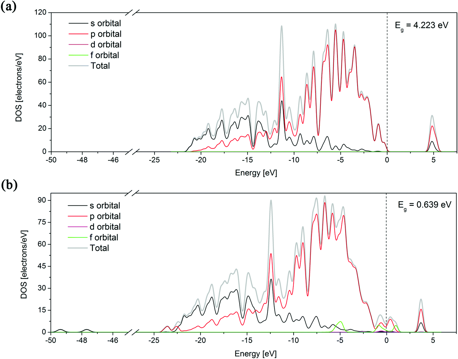 | ||
| Fig. 4 Total and partial density of states for (a) parent diamond structure and (b) the most stable Er:diamond structure with Er in the substitutional position with 3 vacancies in the vicinity. The calculated band gap (Eg) values for the given structure are shown in the right-top corner of the graphs. The dotted vertical line corresponds to the Fermi level (placed at the zero level). | ||
Charge analysis was done using three charge analysis formalisms: Mulliken, Hirshfeld and QEq (for a description see Section 2.1). The calculations were done for the Er-defect in the substitutional position in the diamond structure with various numbers of vacancies and are summarized in Table 6. The charge values are stated in the elementary charge e (approx. 1.6021766208 × 10⁻¹⁹ C50). In the Mulliken charge analysis the trend is that with the increasing number of vacancies the calculated charge decreases from about +3.7 e to +2.58 e. In the Hirshfeld charge analysis the charge was around +0.3 e, having the lowest value for the 2 vacancies of +0.29 e, the highest value for the 3 vacancies of +0.39 e, and for 0, 1, and 4 vacancies a value of +0.32 e. The difference is very high between the two approaches. If one considers the charge neutrality condition for the resulting Er-doped diamond, the carbon atoms in the vicinity of the Er atom with the charge of around +3 from Mulliken analysis would have the total charge of approx. −3 which is a fairly high value for a covalently bonded structure like diamond with all carbon atoms having zero charge. Therefore the value of around +0.3 to +0.4 from Hirshfeld analysis seems to be more reasonable for the real system with the Er defect. The charge equilibration method gave the charge values of around +0.88 e and almost did not change for the different models with various numbers of vacancies. This is probably caused by the fact that the charge equilibration method is mainly used for the molecules and with the very large systems it could not account for the small changes in the vicinity of one atom.
| Structure | Mulliken [e] | Hirshfeld [e] | QEq [e] |
|---|---|---|---|
| Ersub:diamond (0 vacancies) | 3.72 | 0.32 | 0.884026 |
| Ersub:diamond (1 vacancy) | 3.38 | 0.32 | 0.884140 |
| Ersub:diamond (2 vacancies) | 3.04 | 0.29 | 0.884228 |
| Ersub:diamond (3 vacancies) | 2.86 | 0.39 | 0.884224 |
| Ersub:diamond (4 vacancies) | 2.58 | 0.32 | 0.884217 |
3.2 The experimental results of Er:diamond
Three samples of Er-doped single-crystal diamond were prepared and analysed. An overview specifying the conditions of ion implantation is provided in Table 7. For the erbium concentration depth profile determination, the RBS method was used. In Fig. 5a the erbium concentration depth profiles are depicted for the Er:diamond samples prepared by using the ion implantation fluences of 1.0 × 10¹⁴ ions per cm2, 1.0 × 10¹⁵ ions per cm2 and 5.0 × 10¹⁵ ions per cm2. The ion projected range Rp was derived as the mean value of erbium depth profiles determined by RBS and was supposed to obey a Gaussian distribution, while ΔRp was determined by evaluating the profile standard deviation. These values were extracted from the experimental Er-concentration depth profiles and were compared with the predictions given by SRIM simulations, which are summarized in Table 7. The relative concentrations of the disordered atoms ND/N were calculated from the area of the deeper-lying disordered peak (see Fig. 6) using the well-known procedure described in ref. 43. The parameters ND/N were deduced from eqn (5), including the region broader than the surface peak to cover the whole Er implanted layer. The damage accumulation is mainly pronounced in the subsurface region at a channel of about 200 (see Fig. 6) in the aligned spectra (the aligned spectrum is obtained by recording back-scattered ions under the condition that the ion beam is aligned along the main axis of the crystallographic orientation). Thus the average relative disorder density in the estimated layer is lower than that in the subsurface layer where the almost fully disordered structure appeared. | (5) |
| Cut (sample no.) | Ion implantation conditions | R p [nm] | ΔRp [nm] | N D/N [%] | χ D [%] |
|---|---|---|---|---|---|
| SRIM | Er+, 190 keV | 45 | 15 | — | — |
| Parent diamond | — | — | — | — | 13 |
| Z (I-277) | Er+, 190 keV, 1.0 × 10¹⁴ ions per cm2 | 44 | 9 | 46 | 53 |
| Z (I-278) | Er+, 190 keV, 1.0 × 10¹⁵ ions per cm2 | 41 | 12 | 49 | 56 |
| Z (I-279) | Er+, 190 keV, 5.0 × 10¹⁵ ions per cm2 | 44 | 12 | 69 | 73 |
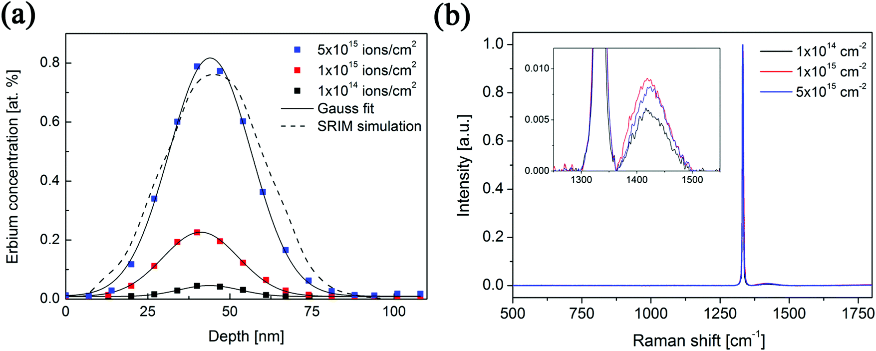 | ||
| Fig. 5 (a) The erbium concentration depth profiles of the prepared Z-cut samples of Er:diamond using different ion implantation fluences. (b) Normalized Raman spectra of the implanted diamond samples. The zoomed spectral region for the non-diamond-based band is shown in the inset. | ||
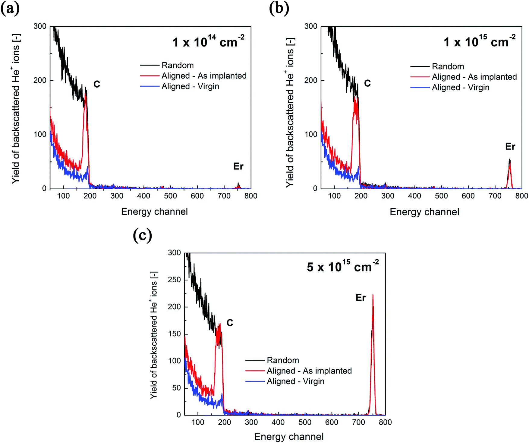 | ||
| Fig. 6 The measured RBS/channelling spectra of Er:diamond samples doped with the ion implantation fluences of (a) 1.0 × 10¹⁴ ions per cm2, (b) 1.0 × 10¹⁵ ions per cm2 and (c) 5.0 × 10¹⁵ ions per cm2. | ||
As expected, the erbium concentrations in the surface layers were increasing according to the increasing ion implantation fluences used. The highest erbium concentrations in the samples of about 0.045 at%, 0.225 at% and 0.800 at% were attained, respectively, for the increasing ion implantation fluences (1.0 × 10¹⁴ ions per cm2, 1.0 × 10¹⁵ ions per cm2 and 5.0 × 10¹⁵ ions per cm2). The mean values of erbium concentration depth distributions in the as-implanted samples were detected at a depth of 41–44 nm below the surface and were in a good agreement with the SRIM simulation.
Fig. 5b compares the Raman spectra of the prepared samples measured in the range of 500–1800 cm−1. Depth analysis by means of Raman spectroscopy is limited by the penetration depth of the laser light in the solid and thus depends on both its wavelength and on the extinction coefficient of the material under investigation. It means that Raman spectroscopy should be both the surface probing technique for analysing graphite and the bulk probing technique for analysing diamond.52 For example, resolving a thin glassy carbon layer on top of the perfect crystalline diamond film is limited, and similarly a low amount of diamond crystals embedded in a non-diamond carbon matrix is hardly resolvable.53 On the other hand, small amounts of graphitic material are easily detected in a diamond matrix due to the higher Raman scattering cross-section of graphite.52 The single-crystal diamond structure has a single peak at 1332 cm−1. The observed broad band at approx. 1400–1450 cm−1 (see the inset in Fig. 5b) can be attributed to the damaged surface layer of implanted diamond samples, i.e. represents either trans-polyacetylene chains at diamond grain boundaries or disordered sp2 bonded carbon within the damaged diamond sub-surface.54 The higher ion implantation fluence resulted in the higher intensity of this band at around 1425 cm−1.
The RBS/channeling measurements showed that the relative numbers of disordered atoms ND/N were about 46%, 49% and 69% for ion implantation fluences of 1.0 × 10¹⁴ ions per cm2, 1.0 × 10¹⁵ ions per cm2 and 5.0 × 10¹⁵ ions per cm2, respectively (see Table 7). Because of the high yields of backscattered ions in the aligned spectra along the chosen crystallographic axes, the RBS/channeling method is very sensitive to the number of structural disordered atoms; therefore, the structural changes in the implanted samples were examined using this method. The measured random and aligned spectra of all three samples are shown in Fig. 6. It follows from these measurements that the density of the disordered atoms – i.e. ND/N – is approximately 50–70% for the samples doped with increasing ion implantation fluence. The fractions of the implanted erbium ions entering substitutional positions after the ion implantation were determined from the change in the area of the erbium depth profiles. At the ion implantation fluences used, no significant preferential substitutional position was observed after ion implantation. It means that a negligible amount of about 5–10% of erbium ions was found in substitutional positions while other erbium atoms were in interstitial positions. Fine scans were carried out, but due to the high degree of structural damage it was impossible to determine the erbium positions in the structure. This effect was expected, as the preferential positioning of the dopant in the highly disordered structure is in fact impossible.
The measured luminescence spectra of X and Z cut Er:diamond samples non-annealed and annealed at the temperatures of 600 °C and 800 °C in a vacuum are shown in Fig. 7. The X cut was doped with the fluence of 1.0 × 10¹⁵ ions per cm2 and the Z cut was doped with the fluences of 1.0 × 10¹⁴ ions per cm2, 1.0 × 10¹⁵ ions per cm2 and 5.0 × 10¹⁵ ions per cm2. All the shown spectra were baseline-corrected to the standard sample and it is therefore able to compare the luminescence intensities of different samples in the spectra. From the luminescence spectra it can be seen that all the samples revealed two main luminescence bands at around 1503 and 1535 nm, whereas the X cut also had two additional luminescence bands at around 1561 and 1585 nm. All the observed luminescence bands correspond to the 4I11/2 → 4I15/2 electronic transitions of Er ions. The luminescence intensities of the Z cut samples were overall very low as compared to the X cut, i.e. the X cut had approximately 6–7 times higher luminescence intensity than Z cut samples. The highest-intensity luminescence in the Z cut was achieved for the lowest used ion implantation fluence of 1.0 × 10¹⁴ ions per cm2 annealed at 800 °C. Measurements of the luminescence spectra of the non-annealed and 400 °C annealed samples showed practically no measurable luminescence for both X and Z cuts. Annealing of the X cut in a vacuum caused a substantial increase of the luminescence intensity – after the annealing at 400 °C no measurable luminescence was achieved, however after the annealing at 600 °C a substantial increase in luminescence was achieved with 4 pronounced luminescence peaks and the annealing at 800 °C only slightly increased (ca. 20–30%) the luminescence intensity while causing no further change to the spectra.
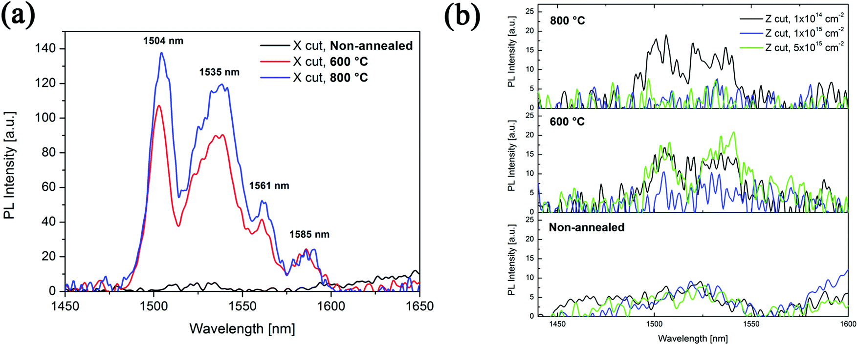 | ||
| Fig. 7 The measured luminescence spectra of Er-doped diamond samples non-annealed and annealed at 600 °C and 800 °C for (a) X cut doped with the fluence of 1.0 × 10¹⁵ ions per cm2 and (b) Z cut doped with the fluences of 1.0 × 10¹⁴ ions per cm2, 1.0 × 10¹⁵ ions per cm2 and 5.0 × 10¹⁵ ions per cm2. | ||
The theoretical and experimental results can be summarized as follows:
(1) According to the theoretical model erbium in the diamond structure occupies substitutional positions rather than interstitial ones. The incorporation of erbium into the diamond structure does not invoke any serious structural changes or broken bonds according to the calculations. The main reason why the substitutional carbon position is more preferred than the interstitial position can be seen when looking on the geometry optimization steps for both structural models where the ability to the relaxation of the structure is a key issue. The interstitial tetrahedral vacancy position has almost no degree of freedom to relax – all the carbon atoms around the vacancy are covalently bonded. On the other hand, when the carbon vacancy is formed, there are several carbon atoms in its vicinity that are just partly bonded (to 3 other carbon atoms) in the diamond structure and therefore are able to move with certain degrees of freedom making more space for the Er atom when incorporated. Therefore, as a result of the model, the structure is more stable if one to three vacant positions are formed in the surroundings of erbium and erbium is displaced in the octahedral vacancy.
(2) Experimental results showed that using the ion implantation doping method it is possible to enrich diamond with erbium with the concentrations from 800 to 8000 ppm. 800 ppm is a value that is mostly found in the materials currently used in photonic amplifying devices (e.g. in the glass fibres there is usually about 500 ppm of erbium, i.e. 0.05 at%). This amount, which does not dramatically increase the optical losses, can be achieved using the ion implantation fluence of 1 × 10¹⁴ ions per cm2. However, the diamond structure is strongly damaged in the ion implantation spot of incidence, it means that 46 to 60 percent of carbon atoms are shifted from their original positions. From this amount only 5 to 10 percent of erbium atoms are situated in the substitutional positions. We found a significantly higher structural damage in the samples implanted by 1 × 10¹⁵ ions per cm2 as compared with the fluence of 1 × 10¹⁴ ions per cm2. This fact was also confirmed by Raman spectroscopy measurements. According to the luminescence measurement it turned out that the post-implantation annealing has a beneficial effect on the luminescence, where after the annealing at the temperature of 800 °C a substantial increase of the luminescence intensity was achieved for the X cut of Er doped diamond samples.
4. Discussion
In the theoretical model, the calculated values of cohesive energies were compared with the experimental ones for pure diamond yielding a very good agreement. The calculation of the band gap of pure diamond is in a good agreement with the previous study of doping of oxygen in diamond25 indicating the good choice of the used DFT functional. Concerning the diamond doping, all the published results obtained by the DFT models dealing with positions of various elements in the diamond structure implicate that the vast majority of used dopants are located in the substitutional carbon sites.23–27 From this point of view it is not surprising that our model involving a large set of atoms predicts the preferential substitutional carbon position for erbium atoms. The only similar study of the doping of lanthanide atoms in the diamond structure was done by the group of A. Magyar et al.23 simulating europium atoms in diamond with a variable number of carbon vacancies and finding the most stable configuration which turned out to be Eu in the substitutional position with one carbon vacancy in the Eu vicinity. This is in a good agreement with our results. The values of defect formation energies for Er in the substitutional position with 1–3 vacancies are comparable with the values calculated for europium. The lowest defect formation energies are around 11 eV for both lanthanides (Eu and Er). Moreover, from our theoretical results for the Er in the substitutional position the three vacancies are even more preferred than one vacancy. We also found that the interstitial position is less favourable than the substitutional carbon position, irrespective of the number of surrounding C-vacancies involved. Obviously the charge balance in the DFT model is rather uncertain. For erbium in the diamond structure with one or three vacancies in its neighbourhood the most probable charge of erbium was calculated to be +0.32 and +0.39, respectively, from the Hirshfeld analysis. This result also corresponds to the value reported in ref. 22, where the europium charge lies between 0 and +1. The details of the band structure around the Fermi level formed by Er-4f states were also analysed in this study. The width of the band gap of Er-doped diamond was lowered to 0.639 eV. A similar lowering was also observed for the Eu and O atoms in the diamond structure.23,25Ion implantation of various elements into the diamond structure has already been a subject of many studies, e.g. the incorporation of N, Si, Ni, Cr, C, Ce, Gd, He and others.2,22,55–57 In these studies various implantation fluences (1 × 10¹⁰–1 × 10¹⁷ ions per cm2) as well as a large range of ion implantation energies (30 keV–2.5 MeV) have been used. The main intention was to form less-defective structures containing a lower concentration of dopants. In our experiments we have intentionally chosen higher fluences, motivated by our previous experience with luminescence measurements of erbium implanted materials using different implantation fluences.58 It is known that in contrast to oxide materials the recovery of the diamond structure is a quite difficult process since the structure tends to amorphise. According to ref. 59 the critical defect density, after which the damaged structure cannot be recovered back to the original diamond structure, is 1 × 10²² vacancies per cm3 (using 52 eV for the displacement energy). It can be seen from the Raman spectra of our samples (Fig. 5b) that a fluence of 1 × 10¹⁴ ions per cm2 yielded a much lower amount of amorphous carbon (according to the broad peak at around 1400–1450 cm−1) in comparison with the other two higher fluences. We therefore suppose that partial healing of this damaged structure can be achieved. Higher fluences however would mean much more serious damage to the structure. Regarding the fact that erbium, being an f-element, is little influenced by the surrounding crystal field in the matrix material due to the shielding of f-orbitals by outer 5s and 5p orbitals, it is by far more important to avoid any non-radiative transitions (from e.g. clustering of atoms) and to have suitable oxidation states of the atoms in the erbium vicinity. This fact brings us to a conclusion that we can expect a reasonably high luminescence even though a part of the diamond sample might be amorphised. In contrast, the defects in the amorphised structure (such as grain boundaries in the NCD diamond) may be even beneficial for the separation of the erbium ions and consequently the higher measurable luminescence.
5. Conclusions
In the present study a theoretical modelling approach was applied to assess the point defect energies in the erbium doped single-crystal diamond structure and compared with the experimental results from the erbium ion implantation into the Z cut 〈001〉 of the single-crystal diamond. The calculated cohesive energy of the parent diamond structure was in a very good agreement with the experimental value, having a difference of approximately 1.0%. According to the theoretical modelling results it turned out that erbium is able to exist in both substitutional and interstitial diamond positions without serious parent-diamond structural changes or bond breakage. Comparing the cohesive and the defect formation energies of the respective structural models, it is found that a more probable erbium location in diamond is the substitutional site of carbon with one or three vacancies in the vicinity of erbium.The ion implantation process caused a substantial damage to the structure of the implanted layers involving up to 69% of atoms being disordered, which prevented the determination of the absolute erbium positions in the crystallographic structure. The prepared Er-doped diamond samples annealed at the temperatures of 400, 600 and 800 °C in a vacuum revealed clear luminescence, whereas the X cut 〈110〉 sample has approximately 6–7 times higher luminescence intensity than the Z cut 〈001〉 sample with the same ion implantation fluence. The reported results are to our knowledge the first demonstration of the Er luminescence in the single crystal diamond structure for the near-infrared spectral region.
Acknowledgements
We acknowledge the Czech Science Foundation project GA 14-05053S and financial support from specific university research (MSMT No. 20/2015). Some parts of the research were realised at the CANAM (Center of Accelerators and Nuclear Analytical Methods LM 2015056) infrastructure. This work was also supported by the MSMT project No. LD15003 (MV, AK) within the frame of the COST Action MP1403 “Nanoscale Quantum Optics”.References
- A. G. A. Grill, Diamond-like carbon coatings as biocompatible materials—an overview, Diamond Relat. Mater., 2003, 12, 166 CrossRef CAS.
- J. F. Prins, Implantation-doping of diamond with B+, C+, N+ and O+ ions using low temperature annealing, Diamond Relat. Mater., 2002, 11, 612 CrossRef CAS.
- N. Tsubouchi, M. Ogura and H. Kato, et al., p-type doping by B ion implantation into diamond at elevated temperatures, Diamond Relat. Mater., 2006, 15, 157 CrossRef CAS.
- R. Kalish, The search for donors in diamond, Diamond Relat. Mater., 2001, 10, 1749 CrossRef CAS.
- T. Sharda, T. Soga and T. Jimbo, Optical properties of nanocrystalline diamond films by prism coupling technique, J. Appl. Phys., 2003, 93, 101 CrossRef CAS.
- C. Manolatou, S. G. Johnson, S. H. Fan, P. R. Villeneuve, H. A. Haus and J. D. Joannopoulos, High-density integrated optics, J. Lightwave Technol., 1999, 17, 1682–1692 CrossRef.
- B. E. Little, J. S. Foresi, G. Steinmeyer, E. R. Thoen, S. T. Chu, H. A. Haus, E. P. Ippen, L. C. Kimerling and W. Greene, Ultra-compact Si–SiO2 microring resonator optical channel dropping filters, IEEE Photonics Technol. Lett., 1998, 10, 549–551 CrossRef.
- V. Prajzler, P. Nekvindova, M. Varga, J. Bruncko, Z. Remes and A. Kromka, Prism coupling technique for characterization of the high refractive index planar waveguides, J. Optoelectron. Adv. Mater., 2016, 18, 915–921 Search PubMed.
- I. Aharonovich and E. Neu, Diamond nanophotonics, Adv. Opt. Mater., 2014, 2(10), 911–928 CrossRef CAS.
- J. O. Orwa, A. D. Greentree and I. Aharonovich, et al., Fabrication of single optical centres in diamond—a review, J. Lumin., 2010, 130, 1646 CrossRef CAS.
- A. Gruber, A. Dräbenstedt, C. Tietz, L. Fleury, J. Wrachtrup and C. Von Borczyskowski, Scanning confocal optical microscopy and magnetic resonance on single defect centers, Science, 1997, 276(5321), 2012–2014 CrossRef CAS.
- A. Beveratos, S. Kühn, R. Brouri, T. Gacoin, J. P. Poizat and P. Grangier, Room temperature stable single-photon source, Eur. Phys. J. D, 2002, 18(2), 191–196 CAS.
- C. D. Clark, H. Kanda, I. Kiflawi and G. Sittas, Silicon defects in diamond, Phys. Rev. B: Condens. Matter Mater. Phys., 1995, 51(23), 16681 CrossRef CAS.
- T. Gaebel, I. Popa, A. Gruber, M. Domhan, F. Jelezko and J. Wrachtrup, New J. Phys., 2004, 6, 98–104 CrossRef.
- I. Aharonovich, S. Castelletto, D. A. Simpson, A. Stacey, J. McCallum, A. D. Greentree and S. Prawer, Two-level ultrabright single photon emission from diamond nanocrystals, Nano Lett., 2009, 9(9), 3191–3195 CrossRef CAS PubMed.
- C. P. Foy, M. C. do Carmo, G. Davies and E. C. Lightowlers, Uniaxial stress measurements on the 0.97 eV line in irradiated silicon, J. Phys. C: Solid State Phys., 1981, 14(1), L7 CrossRef CAS.
- I. Aharonovich, S. Castelletto, D. A Simpson, C. H. Su, A. D. Greentree and S. Prawer, Diamond-based single-photon emitters, Rep. Prog. Phys., 2011, 74(7), 076501 CrossRef.
- D. W. M. Lau, T. J. Karle, B. C. Johnson, B. C. Gibson, S. Tomljenovic-Hanic, A. D. Greentree and S. Prawer, Very bright, near-infrared single photon emitters in diamond, APL Mater., 2013, 1(3), 032120 CrossRef.
- S. Castelletto, A. Edmonds, T. Gaebel and J. Rabeau, Production of multiple diamond-based single-photon sources, IEEE J. Sel. Top. Quantum Electron., 2012, 18(6), 1792–1798 CrossRef CAS.
- I. I. Vlasov, O. Shenderova, S. Turner, O. I. Lebedev, A. A. Basov, I. Sildos and G. Van Tendeloo, Nitrogen and Luminescent Nitrogen-Vacancy Defects in Detonation Nanodiamond, Small, 2010, 6(5), 687–694 CrossRef CAS PubMed.
- E. Ōsawa, Recent progress and perspectives in single-digit nanodiamond, Diamond Relat. Mater., 2007, 16(12), 2018–2022 CrossRef.
- K. Bharuth-Ram, U. Vetter, H. Hofsäss, C. Ronning, M. Dietrich and Isolde Collaboration, Implantation sites of Ce and Gd in diamond, Nucl. Instrum. Methods Phys. Res., Sect. B, 2002, 190(1), 835–839 CrossRef CAS.
- A. Magyar, W. Hu and T. Shanley, et al., Synthesis of luminescent europium defects in diamond, Nat. Commun., 2014, 5, 3523 Search PubMed.
- C. X. Yan, Y. Dai and B. B. Huang, DFT study of halogen impurity in diamond, J. Phys. D: Appl. Phys., 2009, 42(14), 145407 CrossRef.
- M. Ullah, An investigation into the properties of nano crystalline diamond thin films grown by HFCVD system, PhD thesis, University Multan, Pakistan, 2013 Search PubMed.
- M. Ullah, E. Ahmed, F. Hussain, A. M. Rana and R. Raza, Electrical conductivity enhancement by boron-doping in diamond using first principle calculations, Appl. Surf. Sci., 2015, 334, 40–44 CrossRef CAS.
- M. Ullah, E. Ahmed, F. Hussain, A. M. Rana, R. Raza and H. Ullah, Electronic structure calculations of oxygen-doped diamond using DFT technique, Microelectron. Eng., 2015, 146, 26–31 CrossRef CAS.
- R. Kalish, A. Reznik, S. Prawer, D. Saada and J. Adler, Ion-Implantation-Induced Defects in Diamond and Their Annealing: Experiment and Simulation, Phys. Status Solidi A, 1999, 174(1), 83–99 CrossRef CAS.
- S. J. Clark, M. D. Segall, C. J. Pickard, P. J. Hasnip, M. J. Probert, K. Refson and M. C. Payne, First principles methods using CASTEP, Z. Kristallogr., 2005, 220(5–6), 567–570 CAS.
- A. K. Rappe and W. A. Goddard, Charge equilibration for molecular dynamics simulations, J. Phys. Chem., 1991, 95(8), 3358–3363 CrossRef CAS.
- B. Winkler, C. J. Pickard, M. D. Segall and V. Milman, Density functional study of charge ordering in Cs2Au(I)Au(III)Cl6 under pressure, Phys. Rev. B: Condens. Matter Mater. Phys., 2001, 63, 14103 CrossRef.
- M. D. Segall, R. Shah, C. J. Pickard and M. C. Payne, Population analysis of plane-wave electronic structure calculations of bulk materials, Phys. Rev. B: Condens. Matter Mater. Phys., 1996, 54, 16317–16320 CrossRef CAS.
- R. S. Mulliken, J. Chem. Phys., 1955, 23, 1833–1846 CrossRef CAS.
- F. L. Hirshfeld, Bonded-Atom Fragments for Describing Molecular Charge Densities, Theor. Chim. Acta, 1977, 44, 129–138 CrossRef CAS.
- J. Saarilahti and E. Rauhala, Interactive personal-computer data analysis of ion backscattering spectra, Nucl. Instrum. Methods Phys. Res., Sect. B, 1992, 64, 734 CrossRef.
- M. Mayer, SIMNRA version 6.06, Max-Planck-Institut fur Plasmaphysik, Garching, Germany, 2011, http://home.rzg.mpg.de/~mam/.
- IBANDL, http://www-nds.iaea.org/ibandl/GISA.
- H. Shin, S. Kang and J. Koo, et al., Cohesion Energetics of Carbon Allotropes: Quantum Monte Carlo Study, J. Chem. Phys., 2014, 114702 CrossRef PubMed.
- C. Kittel, Introduction to Solid State Physics, Wiley, 1996 Search PubMed.
- G. M. D. Nguimdoa and D. P. Joubert, A density functional (PBE, PBEsol, HSE06) study of the structural, electronic and optical properties of the ternary compounds AgAlX2 (X = S, Se, Te), Eur. Phys. J., 2015, 88, 113 CrossRef.
- H.-P. Komsa, T. Rantala and A. Pasquarello, Comparison between various finite-size supercell correction schemes for charged defect calculations, Physica B, 2012, 407, 3063–3067 CrossRef CAS.
- Y. Li, W. G. Schmidt and S. Sanna, Defect complexes in congruent LiNbO3 and their optical signatures, Phys. Rev. B: Condens. Matter Mater. Phys., 2015, 91, 174106 CrossRef.
- Y. Li, W. G. Schmidt and S. Sanna, Intrinsic LiNbO3 point defects from hybrid density functional calculations, Phys. Rev. B: Condens. Matter Mater. Phys., 2014, 89, 094111 CrossRef.
- R. D. Shannon, Revised Effective Ionic Radii and Systematic Studies of Interatomic Distances in Halides and Chalcogenides, Acta Crystallogr., Sect. A: Cryst. Phys., Diffr., Theor. Gen. Crystallogr., 1976, 32, 751–767 CrossRef.
- From tabulations and averages of C(sp3)–X distances in: F. H. Allen, O. Kennard, D. G. Watson, L. Brammer, A. G. Orpen and R. Taylor, J. Chem. Soc., Perkin Trans. 2, 1987, S1–S19, 10.1039/P298700000S1.
- D. N. Singh, Basic Concepts Of Inorganic Chemistry, Pearson, India, 2010, ISBN: 978-8131728109 Search PubMed.
- X.-H. Hua, J.-H. Xue, L.-M. Yang, Y.-Z. Xu and J.-G. Wua, Butane-1,2,3,4-tetraol-(κ3O1O2O3)(ethanol-κO)tris(nitrato-κ2OO′)erbium(III), Acta Crystallogr., Sect. E: Struct. Rep. Online, 2013, 69(5), 257–258 Search PubMed.
- B. Gyurcsik and L. Nagy, Carbohydrates as ligands: coordination equilibria and structure of the metal complexes, Coord. Chem. Rev., 2000, 203, 81–149 CrossRef CAS.
- L.-M. Yang, X.-H. Hua, J.-H. Xue, Q.-H. Pan, L. Yu, W.-H. Li, Y.-Z. Xu, G.-Z. Zhao, L.-M. Liu, K.-X. Liu, J.-E. Chen and J.-G. Wu, Interactions between Metal Ions and Carbohydrates. Spectroscopic Characterization and the Topology Coordination Behaviour of Erythritol with Trivalent Lanthanide Ions, Inorg. Chem., 2012, 51, 499–510 CrossRef CAS PubMed.
- “CODATA Value: elementary charge”, The NIST Reference on Constants, Units, and Uncertainty. US National Institute of Standards and Technology, June 2015, Retrieved 2016-12-10.
- J. R. Tesmer and M. A. Nastasi, Handbook of Modern Ion Beam Analysis, Materials Research Society, Michigan, 1995 Search PubMed.
- R. E. Clausing, L. L. Horton, J. C. Angus and P. Koidl, Diamond and Diamond-like Films and Coatings, Springer, USA, Boston, 1991 Search PubMed.
- M. Varga, T. Izak, V. Vretenar, H. Kozak, J. Holovsky, A. Artemenko, M. Hulman, V. Skakalova, D. S. Lee and A. Kromka, Diamond/carbon nanotube composites: Raman, FTIR and XPS spectroscopic studies, Carbon, 2017, 111, 54–61 CrossRef CAS.
- F. Klauser, D. Steinmüller-Nethl, R. Kaindl, E. Bertel and N. Memmel, Raman Studies of Nano- and Ultra-nanocrystalline Diamond Films Grown by Hot-Filament CVD, Chem. Vap. Deposition, 2010, 16, 127–135 CrossRef CAS.
- S. Castelletto, I. Aharonovich, B. C. Gibson, B. C. Johnson and S. Prawer, Imaging and quantum-efficiency measurement of chromium emitters in diamond, Phys. Rev. Lett., 2010, 105(21), 217403 CrossRef CAS PubMed.
- L. Himics, S. Toth, M. Veres, A. Toth and M. Koos, Effective implantation of light emitting centers by plasma immersion ion implantation and focused ion beam methods into nanosized diamond, Appl. Surf. Sci., 2015, 328, 577–582 CrossRef CAS.
- P. F. Lai, S. Prawer and L. A. Bursill, Recovery of diamond after irradiation at high energy and annealing, Diamond Relat. Mater., 2001, 10(1), 82–86 CrossRef CAS.
- P. Nekvindova, B. Svecova and J. Cajzl, et al., Erbium ion implantation into different crystallographic cuts of lithium niobate, Opt. Mater., 2011, 34, 652–659 CrossRef.
- C. Uzan-Saguy, C. Cytermann, R. Brener, V. Richter, M. Shaanan and R. Kalish, Damage threshold for ion-beam induced graphitization of diamond, Appl. Phys. Lett., 1995, 67(9), 1194–1196 CrossRef CAS.
Footnote |
| † Electronic supplementary information (ESI) available. See DOI: 10.1039/c6cp08851a |
| This journal is © the Owner Societies 2017 |