
 Open Access Article
 This Open Access Article is licensed under a
 Creative Commons Attribution 3.0 Unported Licence
Molecular and thin film properties of cobalt half-sandwich compounds for optoelectronic application†
Maxwell
Reinhardt‡
a,
Simon
Dalgleish‡
*bc,
Yoshiaki
Shuku
c,
Louisa
Reissig
c,
Michio M.
Matsushita
c,
Jason
Crain
d,
Kunio
Awaga
c and
Neil
Robertson
 *a
*a
aEaStCHEM School of Chemistry, University of Edinburgh, David Brewster Road, Edinburgh EH9 3FJ, UK. E-mail: neil.robertson@ed.ac.uk
bInstitute for Advanced Research, Nagoya University, Furo-cho, Chikusa-ku, 464-8601, Nagoya, Japan. E-mail: s.dalgleish@nagoya-u.jp
cDepartment of Chemistry and Research Center for Materials Science, Nagoya University, Furo-cho, Chikusa-ku, 464-8602 Nagoya, Japan
dSchool of Physics and Astronomy, University of Edinburgh, James Clerk Maxwell Building, Peter Guthrie Tait Road, Edinburgh, EH9 3FD, UK
First published on 10th February 2017
Abstract
The structure and electronic properties of a novel cobalt half sandwich complex of cyclopentadiene (Cp) and diaminonaphthalene (DAnap) [CpCo(DAnap)] are described and compared to the previously reported diaminobenzene derivative [CpCo(DAbnz)] in view of their potential for (opto)electronic device application. Both complexes show stable redox processes, tunable through the diaminoacene ligand, and show strong absorption in the visible region, with additional transitions stretching into the near infrared (NIR). CpCo(DAnap) crystallises with a particularly large unit cell (9301 Å3), comprising 32 molecules, with a gradual rotation over 8 molecules along the long c-axis. In the solid state the balance of the optical transitions in both complexes is reversed, with a suppression of the visible band and an enhancement of the NIR band, attributed to extensive intermolecular electronic interaction. In the case of CpCo(DAnap), highly crystalline thin films could be formed under physical vapor deposition, which show a photocurrent response stretching into the NIR, and p-type semiconductor behavior in field effect transistors with mobility values of the order 1 × 10⁻⁴ cm2 V−1 s−1. The device performance is understood through investigation of the morphology of the grown films.
Introduction
Within the field of organic electronics, transition metal complexes have shown exceptional performance as sensitizers in solar cells1 and as dopants in light emitting diodes,2 and their colligative properties have also shown promise in charge transport applications.3–5 The metal ion can be used to tune the energy levels of an existing ligand framework, such as for the phthalocyanines,6 to impart spin,7 or to affect the molecular or bulk structure through sterics and/or intermolecular interactions.8,9 Alternatively, the metal ion can be used to define the molecular geometry, and to induce new and intense transitions between metal and ligand orbitals.1,2,10 In some cases, the metal ion can also serve to extend the delocalization of the ligand framework over the metallocyclic ring, yielding a non-zero π-character to the M–L bonds. In such cases, distinct molecular orbitals are formed, broadly delocalized over the molecular skeleton, often with a greatly reduced HOMO/LUMO gap and, as such, these complexes have shown promise as stable low bandgap semiconductor materials.3–5The square planar [M(dithiolene)2] complexes (M = Ni, Pd, Pt, Au) serve as model examples of such systems,11,12 and have shown high charge carrier mobilities exceeding 0.1 cm2 V−1 s−1,5 as well as air-stable ambipolar operation,3 and have been employed as photoconductors for photodetector application due to their intense absorption stretching into the NIR.13,14 In addition, the (diimino) o-quinones have also been investigated as semiconductor materials, and Noro et al. have shown ambipolar operation from the Ni(o-diiminobenzosemiquinonate)2 complex, with mobility values > 10−2 cm2 V−1 s−1.4
While most studies have focused on homoleptic systems, heteroleptic complexes offer the possibility of fine tuning the material properties through electronic and/or structural effects. Among these, the half metallocenes (η5-Cp and Cp*) of Co and Ni dithiolenes have been studied in depth by Fourmigué et al.15–18 due to their interesting structural properties resulting from the out-of-plane aromatic η5-Cp(*), coupled with their magnetic properties (Ni),19–21 and the possibility for isostructural spin dilution (Co).22 Alongside the dithiolenes, the half metallocene derivatives of the diimino o-quinones with Co have also been synthesised, and Brill further investigated the structure and bonding within these complexes in the 1980s,23–27 but studies were not pursued much beyond their chemical and structural characterisation.28–31
This study builds on these initial investigations, and focuses on the structure and electronic properties of a novel cyclopentadienyl half-sandwich complex of Co with 2,3-diaminonaphthalene (DAnap), and its potential for (opto)electronic device application. The electronic properties of CpCo(DAnap) are compared through electrochemistry, electronic absorption spectroscopy and computational methods to the related 1,2-diamidobenzene (DAbnz) analogue, the structure of which has previously been reported by Rheingold et al.,25 and the device application of thin films of such complexes to photodetectors is explored. The two compounds that are discussed are shown in Scheme 1.
 | ||
| Scheme 1 Molecular structure of CpCo(DAbnz) and CpCo(DAnap). | ||
Experimental
Synthesis
All reagents were purchased from Sigma-Aldrich and were used without further purification, apart from 1,2-diaminobenzene, which was sublimed before use. The synthesis of CpCo(DAbnz) was derived from the method of Heck et al.29 using (η5C5H5)Co(CO)I230 as precursor. The synthetic procedure for both CpCo(DAbnz) and (η5C5H5)Co(CO)I2 are given in the ESI.†Molecular characterization
Mass spectrometry was carried out using an MS50 instrument. Elemental analyses were performed by Stephen Boyer at London Metropolitan University. Infrared spectroscopy measurements were performed using KBr disks on a JASCO FT/IR-410 spectrophotometer. 1H-NMR and 13C-NMR experiments were performed on a Bruker 500 MHz Fourier transform spectrometer. The solution electronic absorption spectra were recorded with a Jasco V-570 UV/Vis/NIR spectrophotometer in a 1 cm path length quartz cell. Diffuse reflectance spectra were obtained with an integrating sphere attachment, with samples prepared by dilution with barium sulfate (BaSO4) powder.Electrochemical experiments were performed using a standard three-electrode configuration with a μAutolab PGSTAT 30 Type III potentiostat with GPES 4.8 software, with Pt working and counter electrodes. The reference electrode was a double-junction cell of Ag/AgCl and the potentials were corrected vs. the Fc/Fc+ redox couple that occurs at E1/2 = 0.562 V and with ΔE = 110 mV for both compounds. Experiments were carried out with 0.1 M tetrabutylammonium tetrafluoroborate (TBABF4) in acetonitrile (MeCN) solvent. All solutions were degassed with nitrogen for 15 minutes before measurement.
Computational chemistry
Calculations were carried out using the GAUSSIAN 09 package,32 using resources provided by the EaStCHEM Research Computing Facility. Single-molecule gas-phase calculations were performed using initial geometries taken from the single-crystal structures. The B3LYP33,34 hybrid DFT functional, the BP8635,36 functional and the meta-GGA (general gradient approximation) TPSSTPSS37 functional were implemented. The 6-31G(d,p) basis set was used for all atoms apart from the Co atom, which used either an all-electron 6-311G(d,p) basis set or a non-relativistic ECP such as LANL2DZ38–40 or the Stuttgart–Dresden SDD.41 Solvent interactions were represented by using the polarizable continuum model (PCM) with MeCN as the solvent. Time-dependent calculations were run on solvent-optimized structures with the 6-31+G(d,p) basis sets augmented with diffuse functions. Isosurfaces (at 0.05 contour value) of the molecule orbitals were generated using the GAUSSIAN 09 cubegen utility and Arguslab software42 to generate the images that were subsequently rendered using POV-RAY.43 Simulated absorption spectra calculated from TD-DFT were generated using GaussSum 2.2 software44 by a convolution of the energy of the calculated transitions.X-ray crystallography
Single crystals of CpCo(DAnap) suitable for X-ray diffraction were grown by vacuum sublimation (190 °C, 0.2 Pa). Data were acquired with Mo-Kα radiation (λ = 0.71075 Å) on a Rigaku AFC10 Saturn-70 CCD diffractometer at 123 K. Data collection, cell refinement and data reduction were carried out using CrystalClear (version 2.0) software.45 The structure was solved using SIR9746 direct methods, giving the positions of all non-hydrogen atoms, and refined using SHELX47 software and the CrystalStructure (version 4.2.2) structure visualizer48 using a full-matrix least-squares refinement procedure on F2, with non-hydrogen atoms refined anisotropically, and hydrogen atoms placed at calculated positions. Full details of the structure refinement are given in Table S1, ESI.† Molecular graphics were constructed using Mercury49 software.Thin film fabrication
The substrates used for deposition were cleaned immediately before use by mild bath ultrasonication (45 W, 10 min. 0.5% Hellmanix III solution in deionised water, acetone, methanol), and further by UV/air plasma (Bioforce Nanosciences ProCleaner PLUS, 20 min). Where necessary, surface modification was performed immediately after cleaning. HMDS was deposited by heating the substrates in air to 100 °C in a covered Petri dish containing 100 μl HMDS, until all the volatiles had evaporated, and further annealing at 140 °C for 1 h. ODTS was deposited by spin coating, following the method of Ito and co-workers.50 Surface modification was confirmed by contact angle measurements, using a home-built goniometer.51Films of CpCo(DAbnz) and CpCo(DAnap) were fabricated under PVD (ULVAC) at a base pressure of <4 × 10⁻⁴ Pa, with resistance heating of a ceramic crucible to induce sublimation. The growth rate and estimated thickness was monitored using a quartz crystal microbalance (QCM). Solution coated dispersed films of CpCo(DAnap) were formed by spin coating a 2 wt% solution of PMMA in toluene, with different loadings of CpCo(DANap) onto quartz substrates at a rate of 3000 rpm for 60 seconds.
Thin-film absorption measurements on quartz substrates (10 mm × 10 mm) were measured using a Shimadzu UV-3100PC spectrophotometer in transmission mode, with the beam profile reduced using a perforated plate (∅ = 6.5 mm), and with substrates fixed normal to the incident beam. Thickness measurements of the deposited films, formed in an identical manner as for the devices, were performed using a stylus-type step profiler (Dektak 150, scan speed = 4 μm s−1, stylus force = 1 mg) on clean glass substrates. The stylus position was moved after touch-down, because the sample was visibly damaged during this process, but no damage was observed during the scan. At least 3 points were measured, and the results were averaged. The roughness (Ra) of all films was relatively large with Ra values of 10–20 nm, and Rz values of over 50 nm, leading to a relatively large associated error of the measurements. It should be noted, that no pinholes could be observed from these measurements.
The thin film XRD signals were recorded with Cu Kα radiation (40 kV, 30 mA) on a Rigaku Smartlab X-ray diffractometer operated in the 2θ/ω mode scanning the full range 3–80° (step 0.01° at 3° min−1), and at high resolution between 4–16° (step 0.01° at 0.25° min−1). Atomic force microscopy was measured using a Bruker Dimension FastScan AFM system with Fastscan-C Probes (scan area 2 × 2 μm, 0.1–0.3 Hz, 256 or 384 lines for samples; 0.5 × 0.5 μm, 1 Hz, 256 lines for bare substrates) in tapping mode. Images were analyzed using the Nanoscope Analysis software. When necessary the images were level corrected. The surface roughness was determined from at least 3 cross-sections.
Device testing
The substrates for photocurrent measurements were bottom contact interdigitated Pt electrodes on a quartz substrate, deposited by standard photolithographic techniques with S–D channel length of 5 μm (channel width of 32 cm). The wavelength-dependent photocurrent measurements were performed at a bias of 10 V using a tungsten/halogen light source (Spectral Products ASBN-W 100 L) transmitted through a monochromator (Digikröm CM110) covering the 400–1700 nm range, using a 2.4 mm grating in the visible range and a 1.2 mm grating in the NIR (resolution 20 nm) unless otherwise stated (see further Fig. S6, ESI†). The monochromated light power density was determined using a calibrated Si and Ge photodiode. The incident light was mechanically chopped (NF electronic instruments 5584A) at 65 Hz, and the light was focused through a pin-hole (∅ = 2 mm) onto the interdigitated region. The devices were connected to a transimpedance amplifier (Femto, DLPCA200), which was connected to a lock-in amplifier (NF 5610B/A) and an oscilloscope (Tektronix, TBS1052B). The wavelength dependence was recorded using a home-written lab-view program, which allows multiple scans in forward and reverse direction, and any time dependence of the waveform was accounted for by averaging the forward and reverse scans. The responsivity was calibrated from the peak to peak amplitude measured on the oscilloscope.The substrates for transistor measurements were of the bottom-contact, bottom-gate (BCBG) configuration, where the gate electrode was n-doped Si, separated from the S–D electrodes by a 300 nm layer of thermally-grown SiO2. The interdigitated S–D electrodes were made of Pt, deposited by standard photolithographic techniques, with S–D channel length of 10 μm and channel widths of 16 cm. The current–voltage characteristics were measured using a Keithley 2636A sourcemeter, controlled using Labtracer 2.0 software, and were carried out in darkness and under vacuum.
Results and discussion
The general synthetic route to the compounds was derived from the method of Heck,29 who described the synthesis of CpCo(DAbnz), among other chelates of 1,2-disubstituted benzene, by the combination of the ligand with an organometallic precursor in the presence of base. Both complexes were characterised by standard methods, and by X-ray diffraction (XRD) (Fig. S1 and Tables S1, S2, ESI†).Molecular structure and crystal packing
Despite the high solubility of CpCo(DAnap) in common organic solvents, crystals grown by solution methods were of insufficient quality for single crystal analysis. However, large block-shaped crystals could be grown by sublimation under vacuum, and were shown to be isostructural to those grown by solution methods, as measured by powder XRD.52 Crystallographic data and structure refinement details for CpCo(DAnap) are given in Table S1 (ESI†), as well as refinement details for powder samples of both CpCo(DAnap) and CpCo(DAbnz) (Table S2, ESI†). The molecular structure of CpCo(DAnap) is shown in Fig. 1a, and is consistent with that reported for CpCo(DAbnz),25 adopting a T-shaped geometry, with a planar metallocyclic core which is coplanar with the naphthalene ring. The short C–N bond distances (av. = 1.35 Å) suggest considerable π-character to these bonds, and the naphthalene ring shows a pattern of short-long C–C bonds, consistent with an o-naphthoquinone diimine structure. CpCo(DAnap) crystallises in the Pbca space group with an exceptionally large unit cell, containing 32 molecules, and shows an unusual packing behaviour (Fig. 1b), consisting of a racemic mixture of chiral molecular orientation along the c-axis, formed by CH–π interactions. The c-axis is especially long (45 Å) due to a gradual rotation of the molecules by approximately 1.0–7.4° with respect to the LS plane, as defined by the Co and DAnap ligand, resulting in a repeat unit of eight molecules in this direction. Within this perpetual undulation, the orientation of the molecules changes by 180° with respect to the Cp ring face every four molecules, when the angle between adjacent LS planes becomes approximately zero. These undulating chains are orientated to each other in the a-axis by a herringbone packing motif with respect to the LS plane at angles of 57.3 and 63.1° (Fig. 1c). The Herringbone packing is prominent in organic structures that display good charge-transfer properties.53,54 The unique orientation of molecules, with a lack of dimerisation within the unit cell, may translate to the observation of charge-transport properties (vide infra).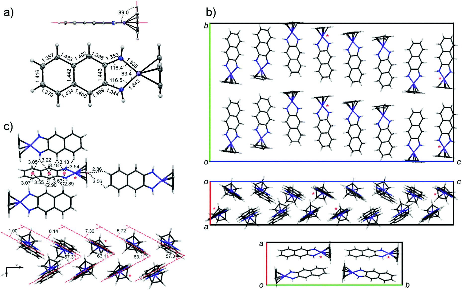 | ||
| Fig. 1 Crystal data for CpCo(DAnap), showing (a) molecular structure with bond lengths and angles; (b) unit cell structure along principle axes a (upper), (b) (middle) and (c) (lower); (c) interconnectivity of molecules. Distances and angles shown in (a) and (c) are for the molecules denoted by an asterisk in (b). | ||
The crystal structure of CpCo(DAbnz), reported by Rheingold et al.,25 (Fig. S2, ESI†) displays a similar interaction between individual molecules as in the structure of CpCo(DAnap), but with an angle closer to 80° between LS planes, and a crystal packing that is notably different, and less simple to define. In both cases, the structure seems to be dominated by CH–π interactions, rather than π–π interactions.
Electrochemistry
The redox activities of CpCo(DAbnz) and CpCo(DAnap) were analysed through both cyclic and differential pulse voltammetry. Cyclic voltammograms of the compounds each display one oxidation and one reduction process in the electrochemical range of −2.0 to 2.0 V vs. Ag/AgCl, seen in Fig. 2 with the measured values in Table S3 (ESI†). The oxidation process occurs at very similar half-wave potentials of −0.13 and −0.10 V for CpCo(DAbnz) and CpCo(DAnap), respectively. This process is electrochemically reversible for CpCo(DAbnz), whereas it is electrochemically irreversible for CpCo(DAnap). Close inspection of the oxidative scan in CpCo(DAnap) reveals a small second anodic process immediately following the first, which is more evident from DPV analysis, as shown in the inset of Fig. 2 (Table S4, ESI†), and is the likely cause of the irreversibility of the oxidation process. The first process could not be decoupled from the second, and thus appeared to be irreversible for all scan windows. | ||
| Fig. 2 Cyclic voltammograms of CpCo(DAbnz) and CpCo(DAnap) showing all processes within the electrochemical window; (inset) differential pulse voltammograms of CpCo(DAbnz) and CpCo(DAnap). | ||
The first reduction process is electrochemically reversible for both compounds, and occurs at more separated half-wave potentials of −1.83 and −1.52 V for CpCo(DAbnz) and CpCo(DAnap), respectively. These data suggest the LUMO orbital to have significant diaminoacene character. From the onset of the redox processes, it is possible to calculate the electrochemically determined energy gap,55 which often corresponds directly to the HOMO–LUMO gap. The energy of the HOMO band can be determined experimentally by referencing it to the E1/2 of ferrocene, using the method of D’Andrade et al.,56 where the HOMO energy is empirically given as EHOMO = (1.4 ± 0.1)·(qVCV) − (4.6 ± 0.08) eV (where q is the electron charge, and VCV is the oxidation potential, relative to Fc/Fc+).
Table 1 reports the electrochemically determined energy levels, where it can be seen that the HOMO levels of both complexes are largely similar, whereas the electrochemically determined gap (and thus the LUMO level) of CpCo(DAnap) is significantly lower than that of CpCo(DAbnz). In both cases, the relatively high HOMO level suggests good Ohmic contact with conventional electrode materials, such as gold or platinum.
| Complex | E CVHOMO (eV) | E DFTHOMO (eV) | E DFTHOMO (eV) | E CVgap (eV) | E Absgap (eV) |
|---|---|---|---|---|---|
| CpCo(DAbnz) | −4.42 | −4.39 | 1.45 | 1.55 | 1.43 |
| CpCo(DAnap) | −4.46 | −4.26 | 1.05 | 1.26 | 1.15 |
Electronic absorption spectra
The solution electronic absorption spectra of both compounds in acetonitrile display one intense absorption in the visible region [λmax = 523 and 560 nm, with ε = 24![[thin space (1/6-em)]](https://www.rsc.org/images/entities/char_2009.gif) 500 and 29820 mol−1 dm3 cm−1, for CpCo(DAbnz) and CpCo(DAnap), respectively], and one very weak NIR absorption [λpeak = 740 and 940 nm, with λonset = 867 and 1078 nm, for CpCo(DAbnz) and CpCo(DAnap), respectively], as seen in Fig. 3a (Table S5, ESI†). The NIR peak shows negative solvatochromism for CpCo(DAnap), where the absorption peak position is blueshifted with increasing solvent polarity, suggesting the transition to involve charge transfer, with the ground state having a larger dipole moment than the excited state (Fig. S3, ESI†). Both of the absorptions are redshifted in CpCo(DAnap) with respect to the same peaks in CpCo(DAbnz). Most notably, the NIR peak is redshifted by ca. 200 nm (2875.2 cm−1), presumably due to the increased conjugation in the diamidonaphthalene ligand of CpCo(DAnap). Both sets of peaks obey the Beer–Lambert law, indicating that the NIR peak is not due to aggregation effects.57 From the onset of the low energy absorption, the optical gap can be estimated at 1.43 and 1.15 eV for CpCo(DAbnz) and CpCo(DAnap) (Table 1), which is slightly smaller than the electrochemically determined gap, as is commonly observed due to the additional interfacial charge barrier in electrochemical measurements.58
500 and 29820 mol−1 dm3 cm−1, for CpCo(DAbnz) and CpCo(DAnap), respectively], and one very weak NIR absorption [λpeak = 740 and 940 nm, with λonset = 867 and 1078 nm, for CpCo(DAbnz) and CpCo(DAnap), respectively], as seen in Fig. 3a (Table S5, ESI†). The NIR peak shows negative solvatochromism for CpCo(DAnap), where the absorption peak position is blueshifted with increasing solvent polarity, suggesting the transition to involve charge transfer, with the ground state having a larger dipole moment than the excited state (Fig. S3, ESI†). Both of the absorptions are redshifted in CpCo(DAnap) with respect to the same peaks in CpCo(DAbnz). Most notably, the NIR peak is redshifted by ca. 200 nm (2875.2 cm−1), presumably due to the increased conjugation in the diamidonaphthalene ligand of CpCo(DAnap). Both sets of peaks obey the Beer–Lambert law, indicating that the NIR peak is not due to aggregation effects.57 From the onset of the low energy absorption, the optical gap can be estimated at 1.43 and 1.15 eV for CpCo(DAbnz) and CpCo(DAnap) (Table 1), which is slightly smaller than the electrochemically determined gap, as is commonly observed due to the additional interfacial charge barrier in electrochemical measurements.58
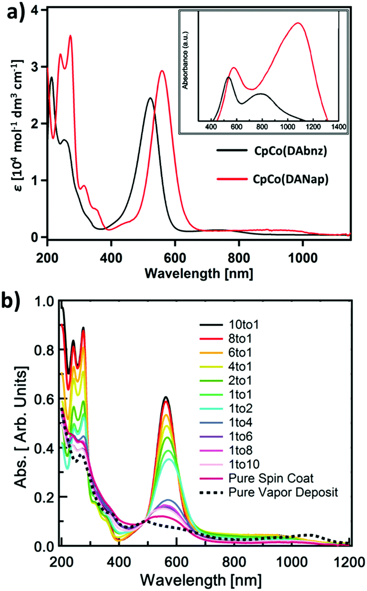 | ||
| Fig. 3 UV/Vis/NIR spectroscopy of (a) CpCo(DAbnz) and CpCo(DAnap) measured in absorption mode in acetonitrile solution and (inset) as diffuse reflection in BaSO4, and (b) thin films of CpCo(DAnap) dispersed at different loading in PMMA matrix (solid lines, PMMA:CpCoDAnap) compared to a vapour deposited film (broken line). | ||
The most interesting aspect of the electronic character of these compounds is revealed from the diffuse reflectance spectra in the solid state. The NIR absorptions, that are weak in the solution spectra, appear with equal or greater intensity to the visible peaks when measured in the solid state, as seen in the inset of Fig. 3a. The peak positions are redshifted from 740 nm to 780 nm in CpCo(DAbnz) and from 940 to 1082 nm in CpCo(DAnap), compared to the solution spectra (Table S5, ESI†). The relative enhancement of the NIR band is also observed in thin films of CpCo(DAnap) deposited by physical vapour deposition (PVD) (vide infra).
To investigate the origin of this phenomenon, dispersion studies of CpCo(DAnap) in a transparent host film of poly(methyl methacrylate) (PMMA) were performed at increasing loading to characterize the role of aggregation on the spectral change. Fig. 3b shows the spectral evolution as the loading of PMMA:CpCo(DAnap) varied from 10:1 to 1:10 in spin-coated films on quartz glass. For comparison, the spectra were normalized based on a common intercept of the solution and thin film spectra (cf. Fig. S13, ESI†). At low loading levels of CpCo(DAnap) (10:1, 8:1), the spectra are essentially a reproduction of that in solution. As the concentration of CpCo(DAnap) increases, the visible band diminishes, which is associated with a broadening and small red shift of the visible peak. Beyond 1:2 loading, the visible peak collapses to reveal an underlying shoulder on the blue edge of the visible peak, which is obscured in the solution spectra. While a small red shift of the NIR band can be observed in the spectra going from 1:10 → pure CpCo(DAnap), the dramatic enhancement in the NIR that is observed in the powder spectra is not observed in the solution coated films at any concentration (Fig. S4, ESI†). It therefore seems that the two changes from solution to solid-state, i.e. the collapse of the visible band (εfilm/εsol@λMAX(Vis) ≈ 15%) and the enhancement of the NIR band (εfilm/εsol@λMAX(NIR) ≈ 250%), are not coupled processes, and might reflect separate characteristics of short-range and long-range order in the films. Alternatively, differing crystallite morphology and film thickness between powder and film may also affect band intensities. In both cases however, electronic effects of intermolecular interactions are clearly shown.
DFT calculations
To shed more light on the nature of the transitions in these complexes, single-molecule gas-phase calculations were performed to determine the ground-state molecular geometry, as well as the position of the frontier orbitals of the molecules. A range of functionals, basis sets and electronic core potentials (ECPs) were tested. The BP8635,36 functional with the 6-31G(d,p) basis set for all ligand atoms and the nonrelativistic LANL2DZ38–40 ECP for Co gave the most accurate result in terms of geometric parameters and frontier orbital energies, when compared to experimental values (Tables S6 and S7, ESI†). Fig. 4 shows the energy levels and molecular orbital (MO) diagrams with percentage occupancies for the relevant frontier orbitals.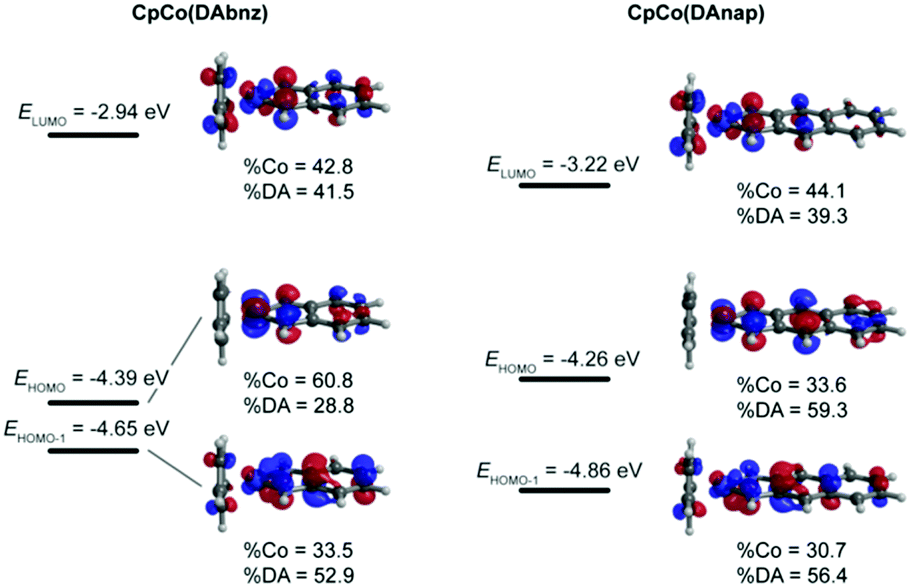 | ||
| Fig. 4 Frontier orbitals (contour cutoff = 0.05) and relative contributions for CpCo(DAbnz) (left) and CpCo(DAnap) (right) calculated by DFT with the BP86 functional, 6-31G(d,p) basis set for ligand atoms and LANL2DZ for Co atoms. | ||
The calculated energy levels for CpCo(DAbnz) are in excellent agreement with experimental data (within 30 meV), but for CpCo(DAnap) calculations performed at the same level of theory underestimate the HOMO energy by 200 meV, and the energy gap by 100 meV, compared to those determined from electrochemical and optical methods, respectively (Table 1). The frontier orbitals are delocalised in both compounds, primarily between the Co centre in DpCo(DAbnz), whereas it is more delocalized onto the diamido ligand in CpCo(DAnap), with a corresponding reduced HOMO–LUMO gap. This delocalisation is an ideal feature for charge transfer applications, as it promotes the potential orbital overlap between molecules, and also improves the stability of charge-transfer states in the solid-state due to lower reorganisation energies.59
The main transitions from time-dependent calculations are exhibited in Fig. S5 and Table S8 in the ESI.† The absorption in the visible region of the spectrum is predicted to be HOMO−1 → LUMO in nature, and the low-energy NIR absorption corresponds to the HOMO → LUMO transition. This assignment agrees with the MO diagrams that indicate that the HOMO−1 and LUMO are very similar in shape and location, thus leading to an intense transition between them. In contrast, the relatively low overlap of the HOMO and LUMO orbitals would account for the weak absorption in the NIR. The good qualitative reproduction of the absorption spectra for both complexes suggests accurate assignment of the electronic transitions, while the difference in the absolute values of the transitions (where the UV and visible peaks energies are overestimated and the NIR peaks are underestimated), might have its origins in solvation effects, as well as the difficulty in computational estimation of the energy of the virtual orbitals, especially in solvatochromic systems.60
Photodetector application
The availability of stable redox levels, delocalised over the molecular skeleton, and the tendency for the materials to interact electronically in the solid state suggests these materials to be potential targets for electronic applications. Furthermore, the presence of a low energy absorption in both complexes is observed in only a low proportion of metal complexes, and the strong and surprising enhancement of the NIR absorption in the solid state makes them interesting candidates for optoelectronic applications using NIR radiation. In order to demonstrate this broad potential, we have studied these as NIR photodetector materials as follows.Both materials readily sublime. However, for CpCo(DAbnz), sublimation under physical vapour deposition (PVD) failed to form adequately uniform thin films for analysis, likely due to the relatively high volatility of the compound, preventing it from depositing stably on the substrates under high vacuum. This was validated by the fluctuations observed in the deposition rate, as monitored by quartz crystal microbalance (QCM). In the case of CpCo(DAnap), highly crystalline thin films could be formed by PVD over a range of substrates. Therefore, efforts were focused on CpCo(DAnap).
In order to assess the photodetector performance of CpCo(DAnap), films of the complex were deposited at 0.2 Å s−1 over interdigitated Pt electrode arrays on quartz substrates (L = 5 μm, W = 32 cm) and subjected to a 10 V bias, and the wavelength dependent conductivity measured in response to monochromatic light over a wavelength range of 400–1700 nm (Fig. S6, ESI†). Initial studies on films of thicknesses <100 nm showed a high failure rate, and so films of 130 nm were targeted. Initially, devices were illuminated from bottom side to avoid potential filtering effects. However, the difference in responsivity depending on illumination direction was observed to be negligible.
In Fig. 5 the photocurrent response to illumination wavelength is plotted. The dominant band in the action spectrum was observed at 484 nm, with a responsivity ∼0.2 mA W−1, corresponding to an external quantum efficiency (EQE) of ∼5 × 10⁻²%. The wavelength of this band coincides with that of the shoulder of the visible peak in the solution spectra, while the main solution band is shown to be silent in the action spectrum. Although the main solution peak is suppressed in the thin-film absorption spectra, it is entirely absent in the photocurrent spectrum, suggesting the HOMO−1 → LUMO to yield a negligible contribution to the photocurrent response. In the NIR region of the action spectrum, an additional band is observed which coincides with the peak originating from HOMO → LUMO transition in the absorption spectrum. The responsivity of this process is rather weak. However, by increasing the light intensity (by using a larger slit) the process can be resolved more clearly. The maximum responsivity in the NIR was calculated to be ∼7 μA W−1 (EQE ∼9 × 10⁻⁴%) at 1040 nm under 10 V bias. Thus, although the responsivity in the visible region is comparable to other pristine organic semiconductors,61,62 the NIR responsivity is significantly lower than those of other transition metal complexes previously examined for NIR photodetector application.13 To further understand the photodetector device performance, the morphology and charge transport properties of CpCo(DANap) films were investigated in more detail.
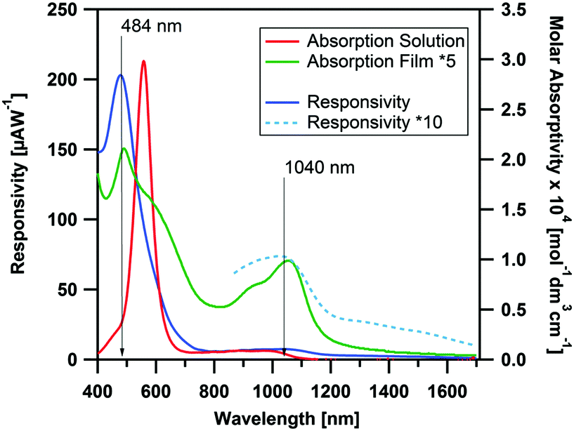 | ||
| Fig. 5 Action spectra of CpCo(DAnap) deposited on interdigitated electrode array (Pt, 5 μm gap at a bias of 10 V between 400–1700 nm), compared to the solution and thin film absorption spectra. | ||
Thin film characterization
The structure and morphology of thin films of CpCo(DAnap) were analysed by XRD, AFM and electronic absorption spectroscopy. Under XRD analysis, films deposited under a range of deposition rates and thicknesses showed two unique out-of-plane diffractions at 2θ = 6.86 and 13.72°, which correspond to d-spacings of ca. 12.9 and 6.5 Å (Fig. 6a and Fig. S7, ESI†). These peaks originate from the 0, 2, 0 and 0, 4, 0 planes in the single crystal, respectively, suggesting a uniaxial orientation, with the ac-axes lying parallel to the substrate. The peak intensity is shown to decrease with deposition rate, suggesting a decrease in the crystallinity of film as the deposition rate increased from 0.2 → 1.5 Å s−1. The peak widths (FWHM), which could be related to the crystallite domain size,63 showed little dependence on deposition rate. Atomic force microscopy (AFM) images of the films deposited at rates of 0.2, 0.7 and 1.5 Å s−1 showed the films to be highly crystalline, with flat rectangular particles of approximate dimensions 500 × 250 × 60 nm for each deposition rate (Fig. 6b–d). For such dimensions, the peak width becomes dominated by instrumental broadening,63 accounting for the similar FWHM values for the films. Comparing the AFM images at different growth rates, it can be seen that the morphology of the particles changes with deposition rate, with the most regular features formed at low deposition rates.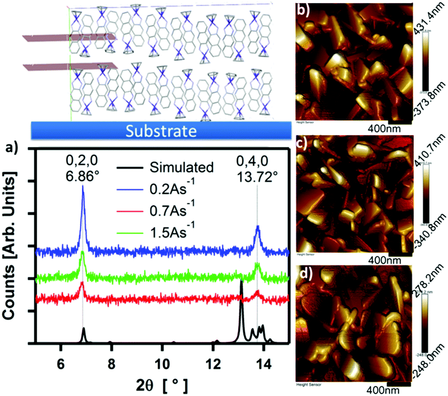 | ||
| Fig. 6 Rate-dependent thin film morphology, showing (a) XRD of a 100 nm film CpCo(DAnap) deposited on SiO2 substrates at rates of 0.2, 0.7 and 1.5 Å s−1, with simulated peaks corresponding to the lattice spacing of the 0,2,0 and 0,4,0 crystallographic planes which lie parallel to the substrate normal (as shown above); (b–d) AFM images of thin films of CpCo(DAnap) deposited at rates of (a) 0.2, (b) 0.7 and (c) 1.5 Å s−1 on SiO2 substrates. | ||
The effect of deposition rate on the charge transport properties of CpCo(DANap) was assessed in field effect transistors fabricated in a bottom contact, bottom gate (BCBG) configuration. CpCo(DAnap) was shown to operate as a p-type semiconductor, as expected from its energy levels. Device reproducibility was improved by surface treating the substrates with hexamethyldisilazane (HMDS) prior to active layer deposition (see ESI†). Fig. 7 shows the output characteristics for 130 nm films formed at different deposition rates. Films deposited at a rate of 0.2 Å s−1 showed a field effect mobility of μ = 1.0 × 10⁻⁴ cm2 V−1 s−1. Increasing the deposition rate of CpCo(DAnap) was shown to significantly deteriorate the mobility (Fig. S8 and Table S9, ESI†), suggesting that the more regular crystallites formed at lower deposition rates were beneficial for charge transport. AFM analysis (Fig. S9–S11, ESI†) reveal that in the early stages of growth, the material deposits as islands growing largely perpendicular to the substrate, before eventually coalescing as the film thickness increases.
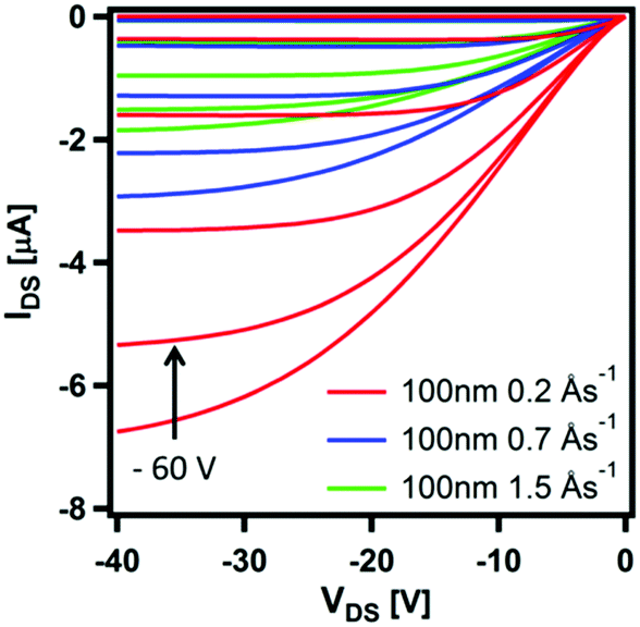 | ||
| Fig. 7 Transfer characteristics (VGS = 0 → −60 V, 10 V steps, VDS = −40 → 0 V, 1 V sweep) of thick films of CpCo(DAnap) deposited on HMDS-treated substrates at different deposition rates. | ||
Conclusions
Cobalt half sandwich complexes of cyclopentadiene and diaminoacenes are shown to have unusual electronic properties, tunable through the acene ligand which lies coplanar with the metallocyclic core. Of particular interest is the observation of NIR absorption in CpCo(DAbnz) and CpCo(DAnap) which originates from a HOMO → LUMO transition between orbitals delocalized, yet spatially separated, over the complex, and which is unexpectedly enhanced in the solid state due to extensive intermolecular interaction. This transition is shown to yield a photocurrent response for CpCo(DAnap) in a planar device architecture. Although the responsivity is relatively low compared to some other literature examples of transition metal complexes, this work provides a first example of NIR optoelectronic application of this family of complexes that could stimulate their further exploration.The mobility values of this material compare reasonably with other small organometallic complexes,3,4 and in order to exploit this class of material to the fullest in both FET and photodetector application, future efforts should be made to improve the morphology of the materials through the use of fabrication methods suited to highly crystalline materials,64 or modification of the molecular unit to suppress island growth, while maintaining the crystallinity and electronic communication between molecules.
Acknowledgements
We thank the EPSRC for funding. This work has made use of the resources provided by the EaStChem Research Computing Facility (http://www.eastchem.ac.uk/rcf), with help from Dr Patricia Richardson. M. R. would like to thank Dr Mark Senn for help with powder XRD refinement. We are grateful to the Ministry of Education, Culture, Sports and Technology (MEXT) of Japan for a Grant-in-Aid for Young Scientists to S. D. (16K17971) and L. R. (16K17853). L. R. would like to thank the JST-ERATO Itami Molecular Nanocarbon Project for use of AFM facilities. This work was additionally supported by the JSPS Core-to Core Program, A. Advanced Research Networks and by the Leverhulme Trust international network award.References
- M. Grätzel, J. Photochem. Photobiol., C, 2003, 4, 145–153 CrossRef.
- H. Xu, R. Chen, Q. Sun, W. Lai, Q. Su, W. Huang and X. Liu, Chem. Soc. Rev., 2014, 43, 3259–3302 RSC.
- T. D. Anthopoulos, G. C. Anyfantis, G. C. Papavassiliou and D. M. de Leeuw, Appl. Phys. Lett., 2007, 90, 122105 CrossRef.
- S. Noro, T. Takenobu, Y. Iwasa, H.-C. Chang, S. Kitagawa, T. Akutagawa and T. Nakamura, Adv. Mater., 2008, 20, 3399–3403 CrossRef CAS.
- L. Qu, Y. Guo, H. Luo, C. Zhong, G. Yu, Y. Liu and J. Qin, Chem. Commun., 2012, 48, 9965–9967 RSC.
- C. G. Claessens, U. Hahn and T. Torres, Chem. Rec., 2008, 8, 75–97 CrossRef CAS PubMed.
- J. Bartolomé, C. Monton and I. K. Schuller, in Molecular Magnets, ed. J. Bartolomé, F. Luisa and J. F. Fernández, Springer-Verlag Berlin Heidelberg, 2014, pp. 221–245 Search PubMed.
- J. D. Baran and J. A. Larsson, Phys. Chem. Chem. Phys., 2010, 12, 6179–6186 RSC.
- Y. Suzuki, M. Fujimori, H. Yoshikawa and K. Awaga, Chem. – Eur. J., 2004, 10, 5158–5164 CrossRef CAS PubMed.
- A. B. P. Lever, J. Chem. Educ., 1974, 51, 612–616 CrossRef CAS.
- G. N. Schrauzer and V. J. Mayweg, J. Am. Chem. Soc., 1962, 84, 3221 CrossRef CAS.
- Progress in Inorganic Chemistry, Dithiolene Chemistry: Synthesis, Properties, and Applications, ed. K. D. Karlin and E. I. Stiefel, Wiley-Interscience, New York, 2003 Search PubMed.
- M. C. Aragoni, M. Arca, M. Caironi, C. Denotti, F. A. Devillanova, E. Grigotti, F. Isaia, F. Laschi, V. Lippolis, D. Natali, L. Pala, M. Sampietro and P. Zanello, Chem. Commun., 2004, 1882–1883 RSC.
- S. Dalgleish, M. M. Matsushita, L. Hu, B. Li, H. Yoshikawa and K. Awaga, J. Am. Chem. Soc., 2012, 134, 12742–12750 CrossRef CAS PubMed.
- M. Fourmigué and V. Perrocheau, Acta Crystallogr., Sect. C: Cryst. Struct. Commun., 1997, 53, 1213–1215 Search PubMed.
- F. Guyon, D. Lucas, I. V. Jourdain, M. Fourmigué, Y. Mugnier and H. Cattey, Organometallics, 2001, 20, 2421–2424 CrossRef CAS.
- M. Nomura and M. Fourmigué, J. Organomet. Chem., 2007, 692, 2491–2499 CrossRef CAS.
- M. Nomura and M. Fourmigué, Inorg. Chem., 2008, 47, 1301–1312 CrossRef CAS PubMed.
- M. Nomura, T. Cauchy, M. Geoffroy, P. Adkine and M. Fourmigué, Inorg. Chem., 2006, 45, 8194–8204 CrossRef CAS PubMed.
- P. Grosshans, P. Adkine, H. Sidorenkova, M. Nomura, M. Fourmigué and M. Geoffroy, J. Phys. Chem. A, 2008, 112, 4067–4073 CrossRef CAS PubMed.
- M. Fourmigué, T. Cauchy and M. Nomura, CrystEngComm, 2009, 11, 1491–1501 RSC.
- M. Nomura, S. Kondo, S. Yamashita, E. Suzuki, Y. Toyota, G. V. Alea, G. C. Janairo, C. Fujita-Takayama, T. Sugiyama and M. Kajitani, J. Organomet. Chem., 2010, 695, 2366–2375 CrossRef CAS.
- E. J. Miller and T. B. Brill, Inorg. Chem., 1983, 22, 2392–2398 CrossRef CAS.
- E. J. Miller, T. B. Brill, A. L. Rheingold and W. C. Fultz, J. Am. Chem. Soc., 1983, 105, 7580–7584 CrossRef CAS.
- A. L. Rheingold, W. C. Fultz, T. B. Brill and S. J. Landon, J. Chem. Crystallogr., 1983, 13, 317–323 CrossRef CAS.
- E. J. Miller, A. L. Rheingold and T. B. Brill, J. Organomet. Chem., 1984, 273, 377–383 CrossRef CAS.
- E. J. Miller, S. J. Landon and T. B. Brill, Organometallics, 1985, 4, 533–538 CrossRef CAS.
- R. F. Heck, Inorg. Chem., 1965, 4, 855–857 CrossRef CAS.
- R. F. Heck, Inorg. Chem., 1968, 7, 1513–1516 CrossRef CAS.
- R. B. King, Inorg. Chem., 1966, 5, 82–87 CrossRef CAS.
- T. Joh, N. Hagihara and S. Murahashi, Bull. Chem. Soc. Jpn., 1967, 40, 661–664 CrossRef CAS.
- M. J. Frisch, G. W. Trucks, H. B. Schlegel, G. E. Scuseria, M. A. Robb, J. R. Cheeseman, G. Scalmani, V. Barone, B. Mennucci, G. A. Petersson, H. Nakatsuji, M. Caricato, X. Li, H. P. Hratchian, A. F. Izmaylov, J. Bloino, G. Zheng, J. L. Sonnenberg, M. Hada, M. Ehara, K. Toyota, R. Fukuda, J. Hasegawa, M. Ishida, T. Nakajima, Y. Honda, O. Kitao, H. Nakai, T. Vreven, J. A. Montgomery, J. E. Peralta, F. Ogliaro, M. Bearpark, J. J. Heyd, E. Brothers, K. N. Kudin, V. N. Staroverov, R. Kobayashi, J. Normand, K. Raghavachari, A. Rendell, J. C. Burant, S. S. Iyengar, J. Tomasi, M. Cossi, N. Rega, J. M. Millam, M. Klene, J. E. Knox, J. B. Cross, V. Bakken, C. Adamo, J. Jaramillo, R. Gomperts, R. E. Stratmann, O. Yazyev, A. J. Austin, R. Cammi, C. Pomelli, J. W. Ochterski, R. L. Martin, K. Morokuma, V. G. Zakrzewski, G. A. Voth, P. Salvador, J. J. Dannenberg, S. Dapprich, A. D. Daniels, O. Farkas, J. B. Foresman, J. V. Ortiz, J. Cioslowski and D. J. Fox, Gaussian 09, Revision B.01, Gaussian, Inc., Wallingford CT, 2009 Search PubMed.
- A. D. Becke, J. Chem. Phys., 1993, 98, 1372–1377 CrossRef CAS.
- C. Lee, W. Yang and R. G. Parr, Phys. Rev. B: Condens. Matter Mater. Phys., 1988, 37, 785–789 CrossRef CAS.
- A. D. Becke, J. Chem. Phys., 1993, 98, 5648–5652 CrossRef CAS.
- J. P. Perdew, Phys. Rev. B: Condens. Matter Mater. Phys., 1986, 33, 8822–8824 CrossRef.
- J. Tao, J. P. Perdew, V. N. Staroverov and G. E. Scuseria, Phys. Rev. Lett., 2003, 91, 146401 CrossRef PubMed.
- P. J. Hay and W. R. Wadt, J. Chem. Phys., 1985, 82, 270–283 CrossRef CAS.
- P. J. Hay and W. R. Wadt, J. Chem. Phys., 1985, 82, 299–310 CrossRef CAS.
- W. R. Wadt and P. J. Hay, J. Chem. Phys., 1985, 82, 284–298 CrossRef CAS.
- P. Fuentealba, H. Preuss, H. Stoll and L. Vonszentpaly, Chem. Phys. Lett., 1982, 89, 418–422 CrossRef CAS.
- M. A. Thompson, ArgusLab 4.0.1, Planaria Software, LLC, Seattle, WA, 2004 Search PubMed.
- Persistence of Vision, Persistence of Vision Pty. Ltd., Williamstown, Victoria, Austrailia, 2004 Search PubMed.
- N. M. O'Boyle, A. L. Tenderholt and M. M. Langer, J. Comput. Chem., 2008, 29, 839–845 CrossRef PubMed.
- R. Corporation, CrystalClear, Rigaku Corporation, Toyko, Japan, 2009 Search PubMed.
- A. Altomare, M. C. Burla, M. Camalli, G. L. Cascarano, C. Giacovazzo, A. Guagliardi, A. G. G. Moliterni, G. Polidori and R. Spagna, J. Appl. Crystallogr., 1999, 32, 115–119 CrossRef CAS.
- G. M. Sheldrick, Acta Crystallogr., 2008, A64, 112–122 CrossRef PubMed.
- R. Corporation, CrystalStructure, Rigaku Corporation, Toyko, Japan, 2010 Search PubMed.
- C. F. Macrae, I. J. Bruno, J. A. Chisholm, P. R. Edgington, P. McCabe, E. Pidcock, L. Rodriguez-Monge, R. Taylor, J. van de Streek and P. A. Wood, J. Appl. Crystallogr., 2008, 41, 466–470 CrossRef CAS.
- Y. Ito, A. A. Virkar, S. Mannsfeld, J. H. Oh, M. Toney, J. Locklin and Z. Bao, J. Am. Chem. Soc., 2009, 131, 9396–9404 CrossRef CAS PubMed.
- G. Lamour, A. Hamraoui, A. Buvailo, Y. Xing, S. Keuleyan, V. Prakash, A. Efekhari-Bafrooei and E. Borguet, J. Chem. Educ., 2010, 87, 1403–1407 CrossRef CAS.
- M. Reinhardt, Metal complexes containing non-innocent ligands for functional materials, Doctoral thesis, University of Edinburgh, UK, 2012 Search PubMed.
- S. C. B. Mannsfeld, A. Virkar, C. Reese, M. F. Toney and Z. Bao, Adv. Mater., 2009, 21, 2294–2298 CrossRef CAS.
- A. J. Lovinger, D. D. Davis, A. Dodabalapur and H. E. Katz, Chem. Mater., 1996, 8, 2836 CrossRef CAS.
- J. L. Brédas, R. Silbey, D. S. Boudreaux and R. R. Chance, J. Am. Chem. Soc., 1983, 105, 6555–6559 CrossRef.
- B. W. D'Andrande, S. Datta, S. R. Forrest, P. Djurovich, E. Polikarpov and M. E. Thompson, Org. Electron., 2005, 6, 11–20 CrossRef.
- R. F. Pasternack, P. R. Huber, P. Boyd, G. Engasser, L. Francesconi, E. Gibbs, P. Fasella, G. Cerio Venturo and L. D. Hinds, J. Am. Chem. Soc., 1972, 94, 4511–4517 CrossRef CAS PubMed.
- Electrochemical Methods: Fundamentals and Applications, ed. A. J. Bard and L. R. Faulkner, John Wiley & Sons, Inc., 2nd edn, 2001 Search PubMed.
- C. R. Newman, C. D. Frisbie, D. A. da Silva, J. L. Bredas, P. C. Ewbank and K. R. Mann, Chem. Mater., 2004, 16, 4436–4451 CrossRef CAS.
- S. Budzák, A. D. Laurent, C. Laurence, M. Medved and D. Jacqemin, J. Chem. Theory Comput., 2016, 12, 1919–1929 CrossRef PubMed.
- K. Petritsch and R. H. Friend, Synth. Met., 1999, 102, 976 CrossRef CAS.
- J. C. Ferrer, J. L. Alonso and S. F. de Ávila, Sensors, 2014, 14, 4484–4494 CrossRef PubMed.
- X-Ray Diffraction: A Practical Approach, ed. C. Suryanarayana and M. G. Norton, Plenum Press, New York, 1998 Search PubMed.
- F. G. del Pozo, S. Fabiano, R. Pfattner, S. Georgakopoulos, S. Galindo, X. Liu, S. Braun, M. Fahlman, J. Veciana, C. Rovira, X. Crispin, M. Berggren and M. Mas-Torrent, Adv. Funct. Mater., 2016, 26, 2379–2386 CrossRef CAS.
Footnotes |
| † Electronic supplementary information (ESI) available: Further details on (i) synthesis, (ii) molecular characterisation, (iii) thin film morphology, and (iv) device measurements. CCDC 1521229. For ESI and crystallographic data in CIF or other electronic format see DOI: 10.1039/c6cp08685c |
| ‡ These authors contributed equally to this work. |
| This journal is © the Owner Societies 2017 |