 Open Access Article
Thermal conductivity of epitaxially grown InP: experiment and simulation†
Juliana
Jaramillo-Fernandez
 *a,
Emigdio
Chavez-Angel
b,
Reza
Sanatinia‡
a,
Himanshu
Kataria§
a,
Srinivasan
Anand
a,
Sebastian
Lourdudoss
a and
Clivia M.
Sotomayor-Torres
abc
aDepartment of Material and Nano Physics, Royal Institute of Technology KTH, Kista, SE-16440, Sweden. E-mail: jjf@kth.se
bCatalan Institute of Nanoscience and Nanotechnology (ICN2), CSIC and The Barcelona Institute of Science and Technology, Campus UAB, Bellaterra, 08193 Barcelona, Spain
cICREA, Passeig Lluìs Companys 23, 08010 Barcelona, Spain
First published on 10th February 2017
Abstract
The integration of III–V optoelectronic devices on silicon is confronted with the challenge of heat dissipation for reliable and stable operation. A thorough understanding and characterization of thermal transport is paramount for improved designs of, for example, viable III–V light sources on silicon. In this work, the thermal conductivity of heteroepitaxial laterally overgrown InP layers on silicon is experimentally investigated using microRaman thermometry. By examining InP mesa-like structures grown from trenches defined by a SiO2 mask, we found that the thermal conductivity decreases by about one third, compared to the bulk thermal conductivity of InP, with decreasing width from 400 to 250 nm. The high thermal conductivity of InP grown from 400 nm trenches was attributed to the lower defect density as the InP microcrystal becomes thicker. In this case, the thermal transport is dominated by phonon–phonon interactions as in a low defect-density monocrystalline bulk material, whereas for thinner InP layers grown from narrower trenches, the heat transfer is dominated by phonon scattering at the extended defects and InP/SiO2 interface. In addition to the nominally undoped sample, sulfur-doped (1 × 1018 cm−3) InP grown on Si was also studied. For the narrower doped InP microcrystals, the thermal conductivity decreased by a factor of two compared to the bulk value. Sources of errors in the thermal conductivity measurements are discussed. The experimental temperature rise was successfully simulated by the heat diffusion equation using the FEM.
1 Introduction
Remarkable advances achieved in the field of silicon photonics in the past decade have paved the way for an integrated optoelectronic platform based on silicon. For example, improved manufacturing paths have enabled the fabrication of low-loss passive devices such as filters, waveguides, beam splitters and combiners, which are now standard available devices.1–4 However, the development of active devices and, in particular, the integration of efficient light sources remain an open engineering challenge as far as heat dissipation is concerned. The successful fabrication of such integrated devices holds the key to accomplishing the long-term dream of the photonics and electronics industries: a fully integrated III–V/Si platform.Hybrid integration of III–V semiconductor optoelectronic devices by wafer bonding has been successfully employed on several devices, such as silicon-based modulators, photodetectors, amplifiers and coherent light sources.5–8 However, monolithic approaches are preferred for long-term, large-scale and low-cost manufacturing of devices with enhanced yields. Yet, there are fundamental limitations to the direct growth of III–V active devices on Si, which involve the strong lattice mismatch and large difference in thermal expansion coefficients between III–V semiconductors and silicon substrates.9–13 These factors result in high density threading dislocations and planar defects such as stacking faults, which ultimately lead to material degradation and shortened device lifetimes. The interaction of phonons with crystallographic defects, interfaces between components and layer boundaries results in higher temperatures in localized volumes, especially when the dimensions of the system are scaled down to the micro and nanometric scales. Thus, the increased scattering events of heat carriers significantly reduce the thermal conductivity and give rise to important thermal issues, primarily stability.14,15 The ability to effectively dissipate heat is therefore a crucial limiting factor in integrated photonic circuit design, due to the fact that device functionality and performance strongly depend on the temperature. In particular, for semiconductor coherent light sources, the yield usually decreases above room temperature while the threshold current increases rapidly with temperature.
To date, few studies have addressed thermal effects in integrated III–V on silicon device-like structures and most of them focus on hybrid (wafer-bonded) devices. Sysak et al.16 analyzed a hybrid laser integration platform from a thermal perspective using thermal impedance measurements and finite element simulations. They conclude that the dominant factor influencing the device thermal impedance is the buried oxide layer, which accounts for about 50% of the total thermal resistance. Lei and co-workers proposed an AlN cladding layer as a possible solution for heat spreading in a hybrid III–V laser on silicon, based on a multiphysics electro-thermo-mechanical model.17,18 Recently, Lucci et al.19 theoretically investigated the thermal issues related to the monolithic or heterogeneous nature of a device. They suggest that monolithically integrated lasers dissipate heat towards the Si substrate more efficiently than their hybrid counterparts, arguing that misfit dislocations due to the III–V/Si heteroepitaxy do not impact significantly on the thermal properties of GaSb/AlSb/Si epitaxial layers in these lasers. Despite the increasing interest in thermal management in III–V semiconductor devices integrated on Si, direct thermal conductivity measurements of the building block components of device-like structures have not been reported so far and remain a challenging task. The main reason is the size of such structures, which is usually in the range of few micrometers. On this scale, traditional techniques used for bulk materials are no longer suitable to describe thermal transport.20 Accurate thermal conductivity determination is thus a pivotal step towards realistic thermal analysis in such structures. In this work, we report an experimental investigation of the thermal conductivity of heteroepitaxial laterally overgrown (ELOG) InP layers on silicon substrates. ELOG is one of the methods among several heteroepitaxial techniques used to grow III–V materials on Si.21–23 It uses a dielectric mask (SiO2 in our case) deposited on the buffer layer patterned with trenches through which the epilayers are grown. The buffer layer, called the seed layer, may contain a high dislocation density, on the order of 109 cm−2. The dielectric mask between the trenches acts as a filter for crystallographic defects, therefore resulting in near defect-free mask–epilayer interfaces, and thus high crystalline quality InP on Si. The dislocation density has been shown3 to be reduced to 6 × 106 cm−2. It can also offer the advantage of integrating the gain medium onto a SiO2/Si/SiO2 waveguide for a monolithic evanescently coupled silicon laser.24 Micro-Raman spectroscopy is used to measure the thermal conductivity of the ELOG InP microcrystals, as a contactless and non-destructive optical technique particularly well suited for studying the thermal properties of micrometric samples with irregular geometries. Since building blocks in functional devices are doped, we extend our study to a doped sample. A thorough analysis of errors in the measurement techniques is presented and the results are successfully simulated by the finite element method (FEM). Based on the experimental results, we analyze the interplay between the ELOG sample size and crystallographic defects on thermal transport for undoped and sulfur-doped InP microcrystals. The impact of our findings on coherent light source integration on Si is discussed.
2 Experimental
2.1 Sample preparation
High quality InP microcrystals were grown on Si by epitaxial lateral overgrowth. This approach for heterogeneous integration involves growing InP laterally from trenches in a mask deposited on a defective InP seed layer on a Si substrate. The patterned mask between the trenches acts as a filter for defects arising from differences in the lattice constants (8%) and thermal expansion coefficients (of about 50%) between InP and Si. In addition, if the trench width is half as much as the mask thickness, the so-called necking effect can filter the defects even in the grown region above the opening (Fig. 1).25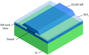 | ||
| Fig. 1 Schematic illustration of the investigated samples obtained by heteroepitaxial growth of InP on Si using the ELOG technique. | ||
The specimens were prepared according to the procedure for heteroepitaxial growth of InP on Si reported elsewhere.26,27 The samples consisted of high-quality epitaxial InP layers grown through trench openings patterned on a 600 nm thick SiO2 mask. The mask was deposited, prior to the epitaxial growth, on a highly defective InP seed layer grown on a Si substrate to accommodate the severely lattice mismatched materials. The width of these openings was varied from 250 to 400 nm to study its influence on crystal growth and the filtering of planar defects and dislocations. In order to have a better understanding of thermal conductivity in device-like structures, we investigated both undoped and sulfur-doped (∼1 × 1018 cm−3) samples. Furthermore, the SiO2 layer was removed by wet etching from the first set of samples in order to evaluate its influence on thermal diffusion.
2.2 Thermal conductivity measurements using the Raman shift method
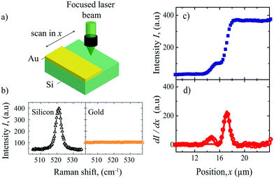
The thermal conductivity of InP microcrystals was measured by the Raman shift method. In standard Raman thermometry experiments, continuous visible light is partially absorbed by a semi-opaque sample, resulting in non-homogenous heating of the probed volume. The analyzed volume is given by V = 4πr2ρ, where r is the radius of the Gaussian focused beam and ρ is the penetration depth of light in the solid.By gradually increasing the excitation power, the power absorbed at the surface increases, inducing a localized non-homogeneous temperature rise. Simultaneously, the light that interacts with the studied sample undergoes Raman scattering, giving rise to a spectrum where the Raman frequencies of optical phonons are red-shifted due to the thermal expansion of the lattice. Owing to the variations in the equilibrium position of the atomic species, the anharmonicity of the bonds results in a variation of the interatomic forces and therefore in the shift of the phonon frequencies.28,29 The resulting temperature-dependent peak positions are then recorded as a function of the absorbed power and compared to a calibration curve that allows the estimation of the weighted average temperature rise in the probed volume. The calibration curve is obtained by externally heating the sample and registering the corresponding vibrational frequencies of the optical phonon modes. A schematic of the set-up used in the backscattering geometry to carry out the thermal conductivity measurements is shown in Fig. 2. An argon ion laser with a wavelength of 532 nm was simultaneously used as a heat source and a temperature measuring probe. The laser light was focused onto the sample surface by a 50× objective with a numerical aperture of NA = 0.55. In Raman thermometry, the main sources of uncertainty on the measured thermal conductivity arise from the uncertainties on the laser beam radius and the power absorbed at the sample surface. These parameters were therefore carefully measured. The radius of the nearly-Gaussian spot was obtained by recording the intensity of the first-order Si Raman peak while scanning the beam across the edge of a gold film deposited on a Si substrate (Fig. 3a).
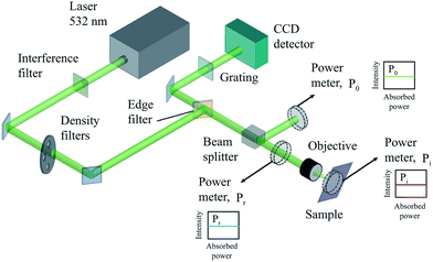 | ||
| Fig. 2 Schematic of the Raman scattering measurement set-up with a built-in array of power meters used for thermal measurements and power absorption characterization. | ||
The intensity of the Si peak was gradually attenuated until it completely disappeared when the spot fully reached the metallic area (Fig. 3b and c). A Gaussian function of the form I·exp(−x2/r2) was used to fit the slope of the intensity I versus position x plot (Fig. 3d), and thus a radius of r = 0.85 μm was determined. From the absorption coefficient of InP at the excitation wavelength of 532 nm (α = 1.01 × 10⁷ m−1), the light penetration depth was estimated to be ρ = 98.7 nm. Since Raman thermometry also requires the accurate determination of the absorbed power at the sample surface, we carried out in situ reflectance and absorbance measurements for various laser powers. The reflectance R, was obtained by measuring the incident Pi and reflected powers Pr, using commercial power meters and considering that R = Pr/Pi. Given the considerable thickness of the InP microcrystals, which varied from 1.5 to 15 μm depending on the trench width, the transmittance was neglected and the absorbance was estimated using the expression A = 1 − R. The inbuilt power meter set-up used for the absorbed power characterization is shown in Fig. 2 in dashed lines. The measured reflectance and absorbance of an InP microcrystal grown on Si through a 250 nm trench are shown in Fig. 4 as an example. The obtained experimental data at 532 nm do not vary within the measured range of absorbed power and match well with the reference values previously reported by Aspnes et al.30 Using the measured absorbance, we estimated that the power absorbed at the sample surface varied from about 3 to 15 mW when the incident laser power increased from about 6 to 22 mW.
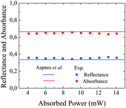 | ||
| Fig. 4 Experimental reflectance and absorbance of an InP microcrystal grown on Si in a 250 nm trench opening on the SiO2 mask. The continuous lines represent the data reported by Aspnes et al.30 for single crystalline InP at 532 nm. | ||
In general, the phonon Raman scattering spectra of zinc blende materials exhibit two peaks corresponding to the longitudinal optical (LO) and transversal optical (TO) phonons with the wave vector k = 0. In bulk InP, the first-order TO and LO Raman peaks have frequencies of 303.7 cm−1 and 345.0 cm−1, respectively.31 To correlate the phonon frequency shifts with the sample temperature rise, we characterized the dependence of the LO Raman shift on the temperature. The sample was placed in a cryostat evacuated to a base pressure of 1 × 10⁻³ mbar. Good thermal contact between the studied specimens and the metallic heating stage was ensured by using silver paint. The linear dependence of the LO frequency on the temperature was obtained in the range from 293 to 363 K and is shown in Fig. 5. For an externally induced temperature rise of 70 K in the microcrystals, a change in the LO frequencies of about 1.2 cm−1 was measured. From the linear fit to the experimental data in Fig. 5, the temperature coefficient of the LO phonon frequency shift was determined as dΔω/dT = −0.0171 cm−1 K−1, which is in good agreement with the specific temperature dependence of the LO mode of dΔω/dT = −0.0168 cm−1 K−1, reported by Irmer and coworkers32 for single-crystalline bulk InP (filled squares in Fig. 5). In addition, we studied a bulk monocrystalline (100) InP substrate to validate the method, which yielded a linear temperature coefficient of dΔω/dT = −0.0165 cm−1 K−1, which is also in good agreement with the previously reported value.
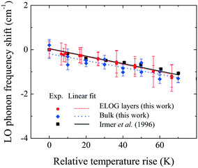 | ||
| Fig. 5 Linear dependence of the InP LO peak position on temperature. The red dots refer to the microcrystals, the blue diamonds to the bulk sample and the black squares to the work of Irmer et al.32 | ||
2.3 Numerical simulation
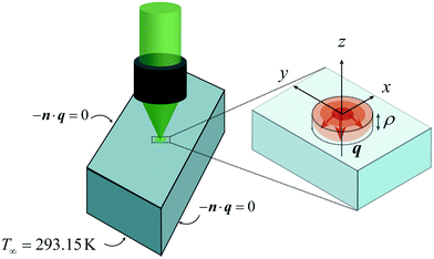
The thermal conductivity of InP microcrystals was obtained by solving the steady-state heat conduction equation for volumetric Gaussian thermal excitation and comparing it to the experimental data. For micrometric samples, an approximate analytical solution is often employed assuming the specimen as a semi-infinite medium with strong absorption at the surface.33–35 Yet, owing to variations in the dimensions of our samples during growth, the microcrystals could not be considered as semi-infinite volumes, particularly when the width of the ELOG InP layers, b, was comparable to the laser spot diameter (2r ≥ b). To account for these effects in the temperature distribution, we solved the three-dimensional (3D) stationary problem of a Raman thermometry experiment by numerical analysis based on the FEM. The physical formulation was developed in Cartesian coordinates such that the x–y plane was defined on the surface of the microcrystal and the incident laser beam was oriented along the z-direction.Assuming that the laser excitation has a Gaussian profile, the volumetric thermal source Q0(x,y) can be written according to the Beer–Lambert law:
 | (1) |
| Q0(x,y) = −∇·(κ∇T) | (2) |
The computation of the boundary fluxes involved solving a system of linear equations derived for each volume element. By using the superposition principle, the temperature field was obtained from these nodal heat fluxes. Knowing the exact dimensions of the InP crystals is of crucial importance for the accurate calculation of the temperature profile via numerical methods. Therefore, the lateral dimensions of each microcrystal were measured by scanning electron microscopy (ZEISS GEMINI ULTRA 55), and the thickness was obtained by optical profilometry (Veeco Wyko NT9300). The measured geometry parameters were used as individual geometrical inputs for the numerical model.
3 Results and discussion
3.1 InP microcrystals: morphology and crystalline quality
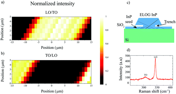
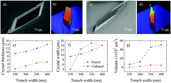
Raman scattering provides a very quick and simple way to determinate the crystalline quality of the material. Typically, the Raman signal is very sensitive to strain,36 sample composition, doping, structural defects,37 crystallographic orientations,38 and pseudo-phases,39 among others. According to Raman selection rules applicable to III–V semiconductors with a zinc blende structure, the TO phonon mode is symmetry-forbidden in (100)-oriented surfaces. In this case, only a sharp and intense LO peak can be observed in the Raman measurements obtained in the backscattering geometry. In general, this peak is used as an indication of the long-range order of the crystal. However, structural disorder, impurities and alloying can break the translational symmetry and activate the TO mode.40 Then, the intensity ratio of the two peaks (LO/TO or TO/LO) provides an indication of the structural defects. Fig. 7 illustrates this, where the intensity ratios of LO/TO (Fig. 7a) and TO/LO (Fig. 7b) of an undoped microcrystal grown through a 300 nm trench are depicted as examples. The high quality of the ELOG InP crystal is demonstrated with the high intensity of the LO/TO ratio, as shown in Fig. 7a. In contrast, the InP seed layer, which is highly defective, is shown to be less intense in the LO/TO ratio but rather intense in the TO/LO ratio, as displayed in Fig. 7b. An estimate of the intensity was obtained by means of a Lorentzian fit of each spectrum with a mean error of ∼10% and 0.03% for TO and LO fitted intensities, respectively. Fig. 7c is a schematic illustration of the specimen cross section and Fig. 7d is a Raman spectrum obtained at Pi = 6 mW, showing the TO and LO peaks for the analyzed sample. Further characterization showing the high quality of the InP crystals, including high resolution X-ray diffraction data and AFM measurements, can be found in the ESI.†Scanning electron microscopy and optical profilometry were used for measuring the dimensions and characterizing the morphology of the grown InP microcrystals. These analyses showed that the trench width strongly affects the crystal growth and defines the dimensions of the microcrystals. From Fig. 8 it can be observed that the crystal thickness, width and volume increase with increasing trench width for both sets of samples. The results also show that doped microcrystals are systematically smaller (Fig. 8e and g) and exhibit slightly different morphologies (Fig. 8c and d) from their undoped counterparts (Fig. 8a and b).
3.2 Thermal properties
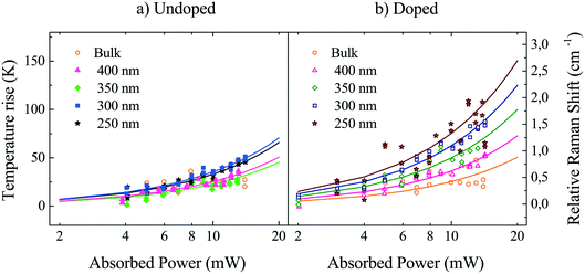
The applicability of the Raman thermometry method to the ELOG layers was first validated on a sample of a bulk monocrystalline (100) InP substrate. The dependence of the relative Raman shift on the power absorbed at the surface of the InP substrate and microcrystals is presented in Fig. 9. Using the calibration curves in Fig. 5, the local temperature rise for each absorbed power can be calculated considering that: | (3) |
A clear trend for both undoped and doped samples emerges from the results presented in Fig. 9. The temperature rise upon light absorption is considerably larger for the microcrystals grown from smaller trenches. This observation can be understood as the result of the reduced dimensions of the crystals grown through narrower trenches, which ultimately leads to smaller effective volumes that can dissipate the heat and thus reach higher temperatures. Regarding the undoped samples, the microcrystals grown through 400 and 350 nm wide trenches have similar temperature rises as the bulk sample, while the ones grown through 250 nm and 300 nm wide trenches show slightly higher temperature rises. Moreover, the doped samples are heated to higher temperatures compared to the bulk substrate and their undoped counterparts. This can be explained by two factors: the small dimensions of the doped crystals and the low thermal conductivity of the 600 nm thick SiO2 layer (κSiO2 = 1.4 W m−1 K−1 (ref. 42)), which promote the heating of the microcrystals.
The experimental values of thermal conductivity measured in the bulk InP substrate, undoped and doped ELOG microcrystals are presented in Fig. 10. These were extracted from the power absorbed at the sample surface, the resulting temperature rise and the solution to the heat diffusion equation solved by the finite element method. Thermal conductivities of 68 ± 4 and 74 ± 8 W m−1 K−1 were obtained for undoped microcrystals grown through trenches of 400 and 350 nm, respectively. The doped sample grown through a 400 nm wide trench also has a thermal conductivity of 68 ± 6 W m−1 K−1. These results, which are very close to the bulk value, constitute evidence of the high crystalline quality of the monocrystalline ELOG samples grown through wider trenches and are in agreement with the temperature rises reported in Fig. 9. The slight overestimation of about 8% for the undoped sample grown though a 350 nm wide trench is within the experimental error, and might be due to the propagation of uncertainties related to the experimental determination of the laser spot size, the optical absorption and sample dimensions.
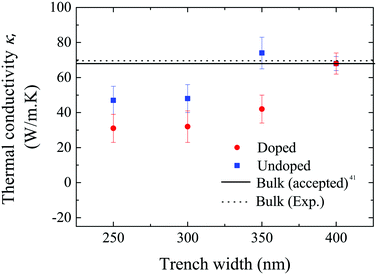 | ||
| Fig. 10 Thermal conductivity of undoped and doped ELOG InP microcrystals as a function of the trench width through which they are grown. The dashed line indicates the measurement of the bulk InP thermal conductivity. The solid line represents the generally accepted value of thermal conductivity for bulk InP.41 | ||
The results in Fig. 10 also suggest that the thermal conductivity of the microcrystals grown through narrower trenches is below the bulk value. For the undoped samples, the thermal conductivity decreased by 31 and 29% as the trench width was reduced to 250 and 300 nm, respectively. Similarly, the thermal conductivity of the doped samples grown though equivalent trench widths showed a decrease of about 54% with respect to the bulk value. On the other hand, the value of the thermal conductivity of the doped sample grown through a 350 nm wide trench implies a reduction from the bulk value of about 38%. These results might seem counterintuitive because it is expected that narrower trenches filter stacking faults and threading dislocations more effectively than the wider ones. However, this depends on the aspect ratio. Junesand and co-workers showed that stacking faults are completely blocked by the SiO2 mask when the aspect ratio of the mask height to the opening width is equal to or larger than 3.9.26 The samples studied here have a maximum aspect ratio of about 2.4, and thus complete dislocation filtering in the samples reported here is disregarded. Transmission electron microscopy studies reported elsewhere26,27 have shown that stacking fault propagation takes place even for narrower trench widths in both undoped and doped samples. In addition, these studies showed that stacking faults do not always reach the surface of the ELOG layers, but appear to be filtered at some point close to the mask opening in the direction perpendicular to the Si substrate, depending on the mask aspect ratio. In a separate study of AlN films on a Si substrate, we have demonstrated43–46 that the contribution to the effective thermal conductivity by phonon scattering at crystallographic defects becomes stronger as the sample thickness decreases. This means that the thermal conductivity is greatly reduced for smaller feature films because phonon scattering at the interface and crystallographic defects dominates thermal transport. Thus, the reduction of the thermal conductivity measured in InP microcrystals grown through narrower trenches (Fig. 10) can be associated with phonon scattering at stacking faults close to the interface between the InP ELOG layer and the SiO2 mask as the dimensions of the microcrystals decrease. On the other hand, the ELOG layers grown though wider openings are much thicker, and the stacking faults are filtered in the region close to the interface with the SiO2 masks. Therefore, the phonon scattering at the interface and crystallographic defects is no longer predominant, but thermal transport is dominated by phonon–phonon scattering, as in bulk single crystalline InP. This observation is supported by the bulk values measured for the thermal conductivities of thicker microcrystals, which are grown through wider trenches, i.e., undoped samples grown through openings of 350 and 400 nm and the doped specimen grown through the 400 nm trench. Based on these results, we propose that thicker and wider ELOG layers, where defects do not reach the surface but are filtered in a region close to the mask opening, are better suited for integration of active devices such as laser sources. The two main advantages are the high thermal conductivity of ELOG InP microcrystals close to the bulk value and a larger effective volume through which heat can be dissipated. On the other hand, thinner ELOG layers in close contact with the SiO2 mask result in much higher temperature rises and therefore are less efficient in removing heat.
4 Conclusions
The thermal conductivity of ELOG InP on silicon has been experimentally investigated via microRaman thermometry. In this work, both undoped and sulfur-doped samples grown through trenches of widths from 250 to 400 nm were studied. The impact of the ELOG layer size and crystallographic defects on thermal transport was analyzed. Our results show that the thermal conductivity of doped and undoped ELOG InP on silicon is very close to the bulk value for samples grown through trenches of 400 nm width. We attribute this to the fact that the samples are thicker and have a lower defect density, consistent with previous work on dislocation filtering. In this case, the thermal transport is dominated by phonon–phonon interactions as in a monocrystalline bulk material. Based on these results, we propose that thicker ELOG microcrystals are better suited for applications involving light source integration due to the higher thermal conductivity and a larger effective volume through which the generated heat is dissipated. The trend and reduction of the thermal conductivity may help to improve thermal analyses in a variety of hybrid integrated opto-electronic circuits.Acknowledgements
This research was supported by the Swedish Research Council VR (grant numbers 349-2007-8664 and 2014-5100) and the Linnaeus Center in Advanced Optics and Photonics (ADOPT). CMST and ECA gratefully acknowledge support from the Spanish MINECO (projects PHENTOM FIS2015-70862-P and nanoTHERM CSD2010-00044), the Catalan AGAUR and the MINECO Severo Ochoa program grant SEV-2013-0295. JJF would like to thank especially Dr. M. Sledzinska and Dr. B Graczykowski for helpful discussions and assistance with the Raman thermometry measurements.References
- J. E. Bowers, T. Komljenovic, M. Davenport, J. Hulme, A. Y. Liu, C. T. Santis, A. Spott, S. Srinivasan, E. J. Stanton and C. Zhang, Proceedings of SPIE, Next-Generation Optical Communication: Components, Sub-Systems, and Systems V, 2016, vol. 9774, pp. 1–18 Search PubMed.
- P. Reithmaier and M. Benyoucefa, ECS Trans., 2016, 72, 171–179 CrossRef.
- W. Metaferia, A. Dev, H. Kataria, C. Junesand, Y.-T. Sun, S. Anand, J. Tommila, G. Pozina, L. Hultman, M. Guina, T. Niemi and S. Lourdudoss, CrystEngComm, 2014, 16, 4624–4632 RSC.
- Y.-T. Sun, H. Kataria, W. Metaferia and S. Lourdudoss, CrystEngComm, 2014, 16, 7889–7893 RSC.
- D. Liang, X. Huang, G. Kurczveil, M. Fiorentino and R. G. Beausoleil, Nat. Photonics, 2016, 10, 1–4 CrossRef.
- J. Michel, J. Liu and L. C. Kimerling, Nat. Photonics, 2010, 4, 527–534 CrossRef CAS.
- G. T. Reed, G. Mashanovich, F. Y. Gardes and D. J. Thomson, Nat. Photonics, 2010, 4, 518–526 CrossRef CAS.
- J. Liu and R. Yang, Phys. Rev. B: Condens. Matter Mater. Phys., 2010, 81, 174122 CrossRef.
- S. Chen, W. Li, J. Wu, Q. Jiang, M. Tang, S. Shutts, S. N. Elliott, A. Sobiesierski, A. J. Seeds, I. Ross, P. M. Smowton and H. Liu, Nat. Photonics, 2016, 10, 307–312 CrossRef CAS.
- Y. Mols, B. Kunert, G. Gaudin, R. Langer and M. Caymax, J. Cryst. Growth, 2016, 452, 244–247 CrossRef CAS.
- F. Gao, L. Wen, X. Zhang, Y. Guan, J. Li, S. Zhang and G. Li, Thin Solid Films, 2015, 589, 32–37 CrossRef CAS.
- F. Gao, L. Wen, Y. Guan, J. Li, X. Zhang, M. Jia, S. Zhang and G. Li, CrystEngComm, 2014, 16, 10721–10727 RSC.
- H. A. Fonseka, H. H. Tan, J. Wong-Leung, J. H. Kang, P. Parkinson and C. Jagadish, Nanotechnology, 2013, 24, 465602 CrossRef CAS PubMed.
- C. K. Majumdar, J. Math. Phys., 1969, 10, 1388 CrossRef.
- A. Iskandar, A. Abou-Khalil, M. Kazan, W. Kassem and S. Volz, J. Appl. Phys., 2015, 117, 125102 CrossRef.
- M. N. Sysak, D. Liang, R. Jones, G. Kurczveil, S. Member, M. Piels, S. Member, M. Fiorentino, R. G. Beausoleil, S. Member and J. E. Bowers, IEEE J. Sel. Top. Quantum Electron., 2011, 17, 1490–1498 CrossRef CAS.
- S. Lei, I. Mathews, J. Camus, S. Bensalem, M. A. Djouadi, A. Shen, G.-H. Duan and R. Enright, 2016 15th IEEE Intersociety Conference on Thermal and Thermomechanical Phenomena in Electronic Systems (ITherm), 2016, vol. 1, pp. 1024–1029 Search PubMed.
- I. Mathews, S. Lei, K. Nolan, G. Levaufre, A. Shen, B. Corbett and R. Enright, Proceedings of SPIE, Integrated Photonics: Materials, Devices, and Applications III, 2015, vol. 9520, pp. 1–10 Search PubMed.
- I. Lucci, C. Cornet, M. Bahri and Y. Léger, IEEE J. Sel. Top. Quantum Electron., 2016, PP, 1–9 Search PubMed.
- D. G. Cahill, W. K. Ford, K. E. Goodson, G. D. Mahan, A. Majumdar, H. J. Maris, R. Merlin and S. R. Phillpot, J. Appl. Phys., 2003, 93, 793 CrossRef CAS.
- Z. Zhou, B. Yin and J. Michel, Light: Sci. Appl., 2015, 4, e358 CrossRef CAS.
- S. Lourdudoss, Curr. Opin. Solid State Mater. Sci., 2012, 16, 91–99 CrossRef CAS.
- Y. B. Bolkhovityanov and O. P. Pchelyakov, Open Nanosci. J., 2009, 3, 20–33 CrossRef CAS.
- Z. Wang, C. Junesand, W. Metaferia, C. Hu, L. Wosinski and S. Lourdudoss, Mater. Sci. Eng., B, 2012, 117, 1551–1557 CrossRef.
- T. A. Langdo, C. W. Leitz, M. T. Currie, E. A. Fitzgerald, A. Lochtefeld and D. A. Antoniadis, Appl. Phys. Lett., 2000, 76, 3700–3702 CrossRef CAS.
- C. Junesand, H. Kataria, W. Metaferia, N. Julian, Y.-T. Sun, J. Bowers, G. Pozina and L. Hultman, Opt. Mater. Express, 2013, 3, 1960–1973 CrossRef.
- H. Kataria, W. Metaferia, C. Junesand, C. Zhang, N. Julian and J. E. Bowers, IEEE J. Sel. Top. Quantum Electron., 2014, 20, 380–386 CrossRef.
- G. Lucazeau, J. Raman Spectrosc., 2003, 4, 478–496 CrossRef.
- T. E. Beechem and J. R. Serrano, Spectroscopy, 2011, 26, 36–44 Search PubMed.
- D. E. Aspnes and A. A. Studna, Phys. Rev. B: Condens. Matter Mater. Phys., 1983, 27, 985–1009 CrossRef CAS.
- D. J. Lockwood, G. Yu and N. L. Rowell, Solid State Commun., 2005, 136, 404–409 CrossRef CAS.
- G. Irmer, M. Wenzel and J. Monecke, Phys. Status Solidi B, 1996, 195, 85–95 CrossRef CAS.
- B. Stoib, S. Filser, J. Stötzel, A. Greppmair, N. Petermann, H. Wiggers, G. Schierning, M. Stutzmann and M. S. Brandt, Semicond. Sci. Technol., 2014, 29, 124005 CrossRef.
- S. Perichon, V. Lysenko, B. Remaki, D. Barbier and B. Champagnon, J. Appl. Phys., 1999, 86, 4700 CrossRef CAS.
- V. Lysenko, S. Perichon, B. Remaki, D. Barbier and B. Champagnon, J. Appl. Phys., 1999, 86, 6841–6846 CrossRef CAS.
- Y. Ogawa, T. Toizumi, F. Minami and A. V. Baranov, Phys. Rev. B: Condens. Matter Mater. Phys., 2011, 83, 081302 CrossRef.
- S. Fuentes, P. Muñoz, P. Barraza, E. Chavez-Angel and C. M. Sotomayor Torres, J. Sol-Gel Sci. Technol., 2015, 75, 593–601 CrossRef CAS.
- T. Muck, W. Wagner, L. Hansen, V. Wagner and J. Geurts, J. Appl. Phys., 2001, 95, 54035407 Search PubMed.
- E. Chávez-Angel, S. Fuentes, R. Zarate and L. Padilla-Campos, J. Mol. Struct., 2010, 984, 131–136 CrossRef.
- R. Cuscó, G. Talamàs, L. Artús, J. M. Martin and G. González-Díaz, J. Appl. Phys., 1996, 79, 3927–3929 CrossRef.
- P. D. Maycock, Solid-State Electron., 1967, 10, 161–168 CrossRef CAS.
- S.-M. Lee and D. G. Cahill, J. Appl. Phys., 1997, 81, 2590–2595 CrossRef CAS.
- J. Jaramillo-Fernandez, J. Ordonez-Miranda, E. Ollier and S. Volz, Phys. Chem. Chem. Phys., 2015, 17, 8125–8137 RSC.
- J. Jaramillo-Fernandez, PhD thesis, Ecole Centrale Paris, 2015 Search PubMed.
- J. Jaramillo-Fernandez, J. Ordonez-Miranda, W. Kassem, E. Oilier and S. Volz, 2015 21st International Workshop on Thermal Investigations of ICs and Systems (THERMINIC), 2015, pp. 1–6 Search PubMed.
- J. Jaramillo-Fernandez, J. Ordonez-Miranda, E. Ollier, R. Sanatinia, H. Kataria, E. Chavez-Angel, S. Volz and C. M. Sotomayor Torres, ECS Trans., 2015, 69, 53–64 CrossRef.
Footnotes |
| † Electronic supplementary information (ESI) available. See DOI: 10.1039/c6ce02642g |
| ‡ Present address: John A. Paulson School of Engineering and Applied Sciences, Harvard University, Cambridge, Massachusetts 02138, USA. |
| § Present address: IRnova AB, Electrum 236, SE-164 40 Kista, Sweden. |
| This journal is © The Royal Society of Chemistry 2017 |

