
 Open Access Article
 This Open Access Article is licensed under a
 Creative Commons Attribution 3.0 Unported Licence
Oligomeric aminoborane precursors for the chemical vapour deposition growth of few-layer hexagonal boron nitride†
Xiaochen
Wang
a,
Thomas N.
Hooper
b,
Amit
Kumar
b,
Isobel K.
Priest
b,
Yuewen
Sheng
a,
Thomas O. M.
Samuels
a,
Shanshan
Wang
a,
Alex W.
Robertson
 a,
Mercè
Pacios
a,
Harish
Bhaskaran
a,
Andrew S.
Weller
*b and
Jamie H.
Warner
*a
a,
Mercè
Pacios
a,
Harish
Bhaskaran
a,
Andrew S.
Weller
*b and
Jamie H.
Warner
*a
aDepartment of Materials, University of Oxford, Parks Road, Oxford, OX1 3PH, UK. E-mail: Jamie.warner@materials.ox.ac.uk
bChemistry Research Laboratories, University of Oxford, Mansfield Road, Oxford, OX1 3TA, UK. E-mail: andrew.weller@chem.ox.ac.uk
First published on 8th December 2016
Abstract
We explore the use of stable, pre-formed, oligomeric aminoboranes as precursors for the chemical vapour deposition growth of few-layered hexagonal boron nitride (h-BN) films on Cu foils under atmospheric pressure conditions. Dimeric diborazane H3B·NH2BH2·NH3 (DAB), and trimeric triborazane H3B·(NH2BH2)2·NH3 (TAB), derivatives of ammonia borane, H3B·NH3 (AB), are compared with AB, a commonly used precursor for the CVD growth of h-BN. Both DAB and TAB show similar effectiveness to AB in growing h-BN few layered films. Using DAB as the precursor instead of AB leads to fully continuous h-BN films in a shorter period of time. Analysis of the surface of the h-BN films reveals that DAB and TAB precursors deposit more nanoparticles on the surface of the h-BN films during their CVD growth within the same time period as when using AB. The viability of these two new h-BN precursors (DAB and TAB), opens up a wider range of solid-state sources for growing wide band gap h-BN films using CVD techniques.
Introduction
Hexagonal boron nitride (h-BN) has attracted considerable interest as a 2D material that is compatible with graphene for future nanoelectronic devices due to their similar hexagonal atomic structure with only 1.7% lattice mismatch. The direct band gap of h-BN is ∼6 eV, making it an insulating 2D crystal that can be used as a substrate for graphene or as a dielectric barrier.1,2 The thickness of the insulating BN film can be controlled by the number of layers in the film, with a single monolayer being the thinnest achievable, at around 0.3 nm. Growing large area continuous films of h-BN is needed for new applications in electronics and opto-electronics. Chemical vapour deposition (CVD) is a leading approach to producing such high quality material.3,4 There are many similarities between the approaches and challenges for growing graphene and h-BN by CVD, as they both can be grown on a Cu foil catalyst and are influenced by the growth temperature, deposition time, and the precursor form.5,6 In both graphene and h-BN CVD synthesis, individual domains nucleate at the beginning and then grow in size until they coalescence to eventually form a complete polycrystalline h-BN film.7 Growing BN is slightly more complex than graphene because the binary structure of h-BN limits the choice of the precursor and it requires precise control of both B and N in the precursor compound to grow high quality h-BN, where graphene only needs a source of carbon and hydrogen.There have been several precursors explored for the growth of BN by CVD, ranging from gases, liquids to solids. For example, Ismach et al. demonstrated the low pressure CVD synthesis of h-BN on sapphire and Ni with controllable thickness using diborane gas (highly toxic, flammable and forms explosive mixtures with air) and ammonia gas (toxic and noxious) as precursors.8 Their experiments suggest that diborane first decomposes to form a Ni–B phase, which then reacts with ammonia, leading to the formation of h-BN. Kidambi et al. and Kim et al. used borazine (B3N3H6) as a precursor for the synthesis of h-BN on Cu substrates using CVD.9,10 They showed that the growth of h-BN on Cu is not limited to a surface mediated growth mechanism, as B can dissolve into Cu and precipitate upon cooling. The solid state precursor H3B·NH3 (AB) has been widely used in the atmospheric pressure CVD (APCVD) synthesis of h-BN.11–14 For gaseous and vaporized liquid precursors, the molecular form of the precursor that arrives close to the substrate for growth might be expected to be similar to the starting precursor, as they are typically not heated to deliver their reactants to the substrate, and ideally approximate to simple “BN” equivalents. In contrast for solid-state precursors, such as AB, they need to be heated to deliver reactants and fragmentation is more likely to occur, thus potentially delivering an ensemble of reactive components compared to the original solid. In particular, H2 loss from AB, encouraged by non-classical B–H⋯H–N hydrogen bonds,15 is first likely to lead to very reactive, transient aminoborane, H2B![[double bond, length as m-dash]](https://www.rsc.org/images/entities/char_e001.gif) NH2,16,17 which then undergoes further dehydrocoupling/oligomerisation/H2-loss processes.18,19 Despite this, solid precursors can have an advantage over liquid and gaseous precursors in the area of chemical stability, such as resistance to oxidization to form borates, and significant advantages with regard to their safe handling in a laboratory environment. However, fragmentation of solid precursors are harder to control during CVD processes because of the larger number of variables that control the local flux of “BN” equivalents to the growth substrate. Liquid and gas precursor flux to the growth substrate in CVD are typically controlled by the mass flow of carrier gases, which can be achieved with great accuracy using digital mass flow controllers. For solid precursors the flux is determined by the heating rate, surface area, and parallel decomposition reactions within the solid that produce new compounds that have higher chemical stability, for example polyaminoboranes.18,19 Given that the studies into using solid-state precursors for h-BN growth are limited, in terms of the different precursor molecular forms, it is important to explore new opportunities in this area. Noting, in particular, that the first fragmentation event in the thermolysis of H3B·NH3 (AB) is loss of H2 to form H2BNH2 we sought stable precursors that acted as masked agents for this very reactive species in the anticipation that this would result in different, possibly enhanced, film-growth. The linear di- and tri-borazanes, H3B·NH2BH2·NH3 (DAB)20 and H3B·(NH2BH2)2·BH3 (TAB)21 reported by Shore and Sneddon respectively offer such a motif. They are air stable solids that can be prepared on a reasonable scale with high purity from readily available starting materials. They offer one and two equivalents of H2BNH2 respectively. DAB and TAB have been predicted to be intermediates in the thermal dehydrogenation of AB.22,23
NH2,16,17 which then undergoes further dehydrocoupling/oligomerisation/H2-loss processes.18,19 Despite this, solid precursors can have an advantage over liquid and gaseous precursors in the area of chemical stability, such as resistance to oxidization to form borates, and significant advantages with regard to their safe handling in a laboratory environment. However, fragmentation of solid precursors are harder to control during CVD processes because of the larger number of variables that control the local flux of “BN” equivalents to the growth substrate. Liquid and gas precursor flux to the growth substrate in CVD are typically controlled by the mass flow of carrier gases, which can be achieved with great accuracy using digital mass flow controllers. For solid precursors the flux is determined by the heating rate, surface area, and parallel decomposition reactions within the solid that produce new compounds that have higher chemical stability, for example polyaminoboranes.18,19 Given that the studies into using solid-state precursors for h-BN growth are limited, in terms of the different precursor molecular forms, it is important to explore new opportunities in this area. Noting, in particular, that the first fragmentation event in the thermolysis of H3B·NH3 (AB) is loss of H2 to form H2BNH2 we sought stable precursors that acted as masked agents for this very reactive species in the anticipation that this would result in different, possibly enhanced, film-growth. The linear di- and tri-borazanes, H3B·NH2BH2·NH3 (DAB)20 and H3B·(NH2BH2)2·BH3 (TAB)21 reported by Shore and Sneddon respectively offer such a motif. They are air stable solids that can be prepared on a reasonable scale with high purity from readily available starting materials. They offer one and two equivalents of H2BNH2 respectively. DAB and TAB have been predicted to be intermediates in the thermal dehydrogenation of AB.22,23
Here, we examine the use of these two B–N precursors DAB and TAB and compare them with AB for growth of h-BN films on Cu by APCVD method. We investigate the morphology of h-BN films as a function of growth time. These AB, DAB and TAB precursors lead to a notable dependence in the film coverage for various growth times. The h-BN films are characterized by transmission electron microscopy (TEM), Raman spectroscopy, atomic force microscopy (AFM), optical microscopy, and scanning electron microscopy (SEM).
Results and discussion
Fig. 2 shows the SEM images of the samples on Cu for the three different precursors (AB, DAB and TAB) with different growth times (10 min, 15 min and 30 min). For AB, Fig. 2a–c, 10 minutes growth resulted in h-BN domains (Fig. S1a†), and for the 15 and 30 minutes growth a complete film is produced. The change from 10 to 15 minutes growth duration with the AB precursor results in a significant increase in the film coverage from single h-BN domains to a continuous film, similar to a recent report, which indicated that longer growth times results in h-BN crystals coalescing with subsequent growth into a complete film.14 The diborazane precursor, DAB, resulted in continuous h-BN films on the Cu substrate, Fig. 2d–f, for all three growth durations: 10 minutes, 15 minutes, and 30 minutes, respectively. The triborazane precursor, TAB, did not produce any h-BN within the 10 and 15 minutes growth periods, Fig. 2g and h, however after 30 minutes growth time a fully continuous h-BN film on the Cu substrate was obtained, Fig. 2i. Different contrast within the SEM images is attributed to slight variations in the layer thickness. In addition to the 30 minutes growth time, small triangular h-BN domains are observed for all three precursors above the grown h-BN film (see Fig. S4†), this could possibly be because the growth mode follows the combination of a layer by layer growth and island growth, similar to the previously described reports.13,24 The CVD grown h-BN films all have white nanoparticles deposited onto the surface which are presumed to be polyaminoborane24 arising from the dehydrocoupling of the precursors, such a H2BNH2,25 as shown in Fig. 2.
Comparing results from all three precursors in the 10 minutes growth window, Fig. 2a, d, and g, shows h-BN domains for the AB precursor, a fully continuous film for the DAB, and nothing for the TAB. This provides insights into the different reactivity of these three precursors and surprisingly doesn't follow a simple trend with increasing molecular weight. The thermal decomposition of AB is quite complex, but is well studied,18 and results in borazine (B3N3H6), transient aminoborane (H2BNH2) and hydrogen gas.26,27 The major volatile products are then delivered into the growth furnace for further reactions at high temperature (1040 °C), resulting in the formation of h-BN film on Cu substrates, as illustrated in Fig. 1b. The byproducts are likely polyaminoborane and noncrystalline polyiminoborane.28 The proposed mechanistic details of dehydrogenation of all the precursors is based on transient and reactive H2BNH2, which then undergoes metal catalyst mediated B–N coupling at the Cu-substrate surface.29–32 The morphology of the CVD grown h-BN on Cu substrates using the precursors DAB and TAB is different compared with h-BN grown using ammonia borane. In terms of the growth rate, the DAB is the most active precursor; while the TAB is the least active precursor. We repeated the growth several times for each precursor and obtained similar results each time, confirming the reproducibility of the experimental synthesis methods with different precursors.
 | ||
| Fig. 1 Atmospheric pressure CVD synthesis of h-BN on a Cu substrate using three different chemical precursors. (a) Structure of h-BN grown precursors, as H3B·NH3, H3B·NH2BH2·NH3 (DAB)19 and H3B·(NH2BH2)2·BH3 (TAB). (b) AB precursors are thermally decomposed into equivalents or derivatives of H2BNH2 and produce h-BN and polyaminoborane via dehydrocoupling. (c) APCVD experimental setup for h-BN growth; the precursor is in an isolated chamber with a valve to control the vapour gas; the chamber is surrounded by a separate heating belt. Cu substrates are placed at the middle of a 1 inch quartz tube. | ||
Further insight into the degree of h-BN coverage on the Cu substrate after CVD growth can be obtained by heating the samples in air to oxidize any region of Cu-substrate that is not covered by h-BN. This approach has been utilized before for graphene layers grown on Cu by CVD. Fig. 3 shows optical microscope images of the baked Cu foils for 10 minutes, 15 minutes, and 30 minutes CVD growth, respectively. These h-BN grown samples are placed on a hot plate and baked at 200 °C for 2 minutes in air. The optical images are complimentary to the SEM images shown in Fig. 2. Oxidization of the Cu results in a colour change from orange to red forming a layer of CuO on the original surface, and thus enables convenient optical analysis of the large area h-BN coverage, as demonstrated in Fig. 3b, d, e, g, h, and j. All samples that showed continuous film coverage in the SEM of Fig. 2, show no signs of Cu oxidization in Fig. 3, confirming that the h-BN films are present across the large areas and protect the Cu from reacting in air.
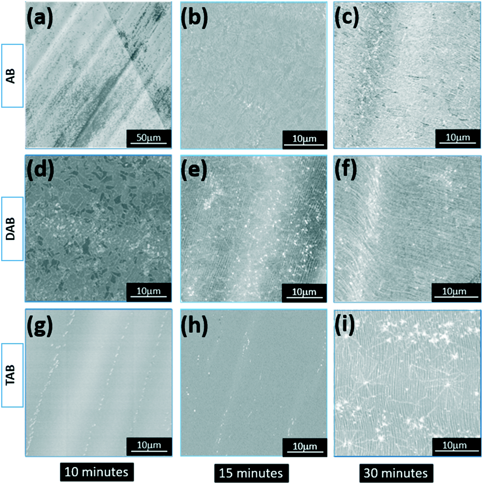 | ||
| Fig. 2 SEM images of the Cu substrate surface after h-BN CVD growth for various durations and with the AB (a–c), DAB (d–f), and TAB (g–i), three different molecular weight precursors, respectively. The x-axis represents the growth time i.e. 10, 15, and 30 minutes and the y-axis represents precursor type i.e. AB, DAB, and TAB. | ||
 | ||
| Fig. 3 Optical images of oxidized Cu surfaces after the CVD growth of h-BN with various growth time and types of precursor. AB grown h-BN on Cu with (a) 10 min, (d) 15 min, and (g) 30 min growth time. DAB grown h-BN on Cu with (b) 10 min, (e) 15 min, and (h) 30 min growth time. TAB grown h-BN on Cu with (c) 10 min, (f) 15 min, and (i) 30 min growth time. | ||
It is also important to examine the deposition of the proposed BN-containing nanoparticles on the surface of the h-BN films. Fig. 4a–c shows SEM images of CVD grown h-BN films for 30 minutes growth time, which are used to analyze the coverage of the surface nanoparticles. As discussed earlier, these nanoparticles are likely formed by dehydrocoupling of the chemical precursors i.e. polymeric aminoborane.28,33Fig. 4g shows the statistical information about the relationship between the precursor type and the coverage of surface nanoparticles, obtained from the images in Fig. 4d–f, where the nanoparticles are white in color. The overall surface nanoparticle coverage is proportional to the precursor molecular weight. For example the ammonia borane grown h-BN film has 5% coverage of the nanoparticle, the DAB grown h-BN film has about 15%, and the trimer grown h-BN film has the highest impurity coverage which is 25%. During this CVD synthesis of h-BN, the trimer precursor is likely producing a larger amount of polyaminoborane compared to the DAB and the ammonia borane precursor.
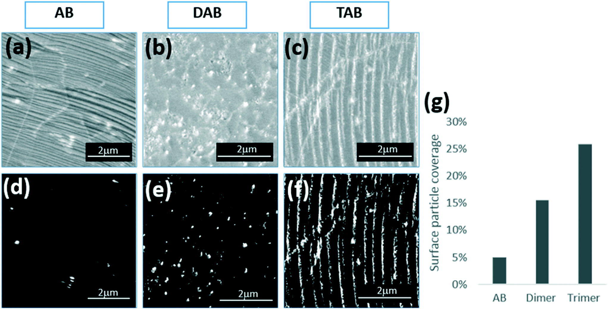 | ||
| Fig. 4 SEM images (a–c) of synthesized continuous h-BN films with ammonia borane, DAB, and TAB precursors and 30 minutes growth time, respectively. Binary threshold SEM images (d–f) of the corresponding surface nanoparticles are shown in white colour. (g) Plot showing the precursor type dependent surface nanoparticle coverage. | ||
To examine the quality of the h-BN films, Raman spectroscopy and atomic force microscopy (AFM) were performed after transferring on to Si substrates with a 300 nm oxide layer. Raman spectroscopy is a powerful technique to analyse the characteristics of 2D materials including h-BN layers. It is well known that the Raman peak of bulk of h-BN is at 1366 cm−1 and shifts to a higher frequency as the number of h-BN layers decreases.34 For a monolayer h-BN film the peak is around 1370 cm−1. All three BN films grown showed Raman spectra with h-BN peaks, Fig. 5a, with the E2g phonon vibrational modes between 1366–1369 cm−1, indicating few layer h-BN. As shown in Fig. 5a, the Raman peaks are symmetric and have narrow width, indicating a h-BN film since the deleterious byproducts of precursor CVD, i.e. cubic-BN, BxCyNz and BN nanoparticles, have been shown to lead to an asymmetric Raman peak position.11,35 Gaussian curve fitting was used to show the symmetry of the three Raman peaks obtained from different precursor grown h-BN films. The FWHM value (14 cm−1) of DAB-grown h-BN film is the lowest compared to the trimer (FWHM = 20 cm−1) and ammonia borane (FWHM = 16 cm−1) grown h-BN. Although Fig. 4 estimates the highest nanoparticle coverage of the whole film for TAB precursor, ∼25%, 75% of the grown h-BN film is not covered by nanoparticles and the Raman spectra show signals primarily from h-BN material. The wet chemical transfer method may help remove the byproducts i.e. BxCyNz and BN nanoparticles. The thickness of the as grown h-BN films was further characterized by atomic force microscopy (AFM). Fig. 5c, e, and g provide AFM height profiles from the measured edges of the transferred h-BN film. The thickness of the ammonia borane grown h-BN film is ∼4 nm, and the thickness of DAB and TAB precursor grown h-BN film are both ∼7 nm, indicating that all the grown h-BN films from these precursors are few-layered.
 | ||
| Fig. 5 (a) Raman spectra of h-BN films transferred to Si substrates with 300 nm oxide grown by AB, DAB, and TAB, respectively. AFM images of h-BN films transferred to Si substrate, (b) TAB grown h-BN sample, (d) DAB grown h-BN sample, and (f) AB grown h-BN sample. Corresponding height profiles (c) for TAB, (e) for DAB, and (g) for AB samples and are taken form the white lines indicated in the corresponding AFM images, respectively. | ||
The layer number was further investigated using transmission electron microscopy (TEM) to image the back folded edge regions of the 30 minute grown h-BN films with the three different precursors. Imaging folded edges provides lines of contrast that enable the counting of the number of layers. The TEM images, Fig. 6b, e, and h, show 2 lines of contrast typical for AB grown samples and 3 lines of contrast for the DAB samples, and 4 lines of contrast for TAB samples. The line profiles taken across these edges, Fig. 6c, f, and i, confirm this. Fig. S9 in ESI† present the statistical variation in the edge number for these samples, showing a distribution. The AFM in Fig. 5 shows the AB films are thinner than the DAB and TAB grown films and the TEM imaging in Fig. 6 supports this. This also supports the Raman spectroscopy results that indicated the h-BN films were few-layered rather than monolayered. The crystalline structure of the h-BN films were characterized using selected area electron diffraction (SAED) taken from the regions shown in the corresponding low-magnification TEM images in Fig. 7a and c for AB precursor, Fig. 7e and g for DAB precursor, and Fig. 7i and k for TAB precursor samples. The SAED patterns show a symmetric hexagonal diffraction pattern, indicative of h-BN lattice structure.28 A single crystal SAED pattern was typically found for AB grown h-BN, seen in Fig. 7b and d. The SAED pattern of DAB and TAB precursor grown h-BN films shows both single and multiple sets of diffraction spots rotated with respect to each other, Fig. 7f and h for DAB precursor, and Fig. 7j and l for TAB precursor, indicating some turbostratic stacking is occurring. The observed interlayer distance in all the h-BN films is ∼3.5 Å, which is similar to that of bulk h-BN.36
 | ||
| Fig. 6 TEM images showing the number of layers of h-BN in the films by imaging their folded edges. Low-magnification TEM images shows the folded edges of (a) AB, (d) DAB, and (g) TAB precursor 30 minutes grown h-BN film. (b, e, and h) are the zoomed-in regions marked in (a, d, and g), respectively. The line contrast line intensity profiles (c, f, and i) record along the marked regions in (b, e, and h). The black arrows point to the counted layers of folded h-BN film. | ||
 | ||
| Fig. 7 Low-magnification TEM images of three precursor grown h-BN films with their corresponding SAED patterns. Low-magnification TEM images of (a and c) AB precursor 30 minutes grown h-BN sample and single set of SAED patterns (b and d). TEM images (e and g) show DAB precursor 30 minutes grown h-BN samples and single crystal and multiple sets of SAED patterns (f and h), respectively. TEM images (i and k) shows TAB precursor 30 minutes grown h-BN samples and single crystal and multiple sets of SAED patterns (j and l), respectively. | ||
Conclusions
In summary, we have synthesized few-layered h-BN films on Cu substrates by the APCVD method using three different precursors. Two precursors, diborazane, H3B·NH2BH2·NH3 (DAB), and trimeric triborazane, H3B·(NH2BH2)2·NH3 (TAB), both derivatives of ammonia borane, H3B·NH3 (AB), show success in growing h-BN. When comparing the resulting h-BN film growth morphology with the AB precursor, 30 minutes growth duration results in continuous h-BN film formation on Cu substrates for all the precursors. The overall surface nanoparticle coverage shows dependence of the precursor molecular weight. The grown h-BN films are characterized via Raman microscopy, AFM, and TEM, indicating that the grown h-BN films are 2–5 nm thick and crystalline. Because the surface of Cu is the same for all three precursors, we can link the difference in growth rates to different precursor decomposition processes. The main driving factor controlling the variable growth will be the molecular gaseous species emitted from the heated precursors, in terms of its chemical structure and rate of emission. Future work incorporating mass spectroscopy to measure the chemical species emitted from each solid state precursor upon heating may help shed more light on this topic. This work offers an insight into the variety of precursors that can be used for the CVD growth of h-BN.Experimental section
Chemical vapour deposition growth of BN
To synthesize h-BN on Cu (Alfa Aesar) substrates at ambient pressure, three types of precursors are used and a 1 inch quartz tube atmospheric pressure CVD system with separated heating belt for the BN precursor is used. Fig. 1a shows the chemical structures of the precursors, they are ammonia borane (≥97%, Sigma-Aldrich). Diborazane, H3B·NH2BH2·NH3 (DAB),20 and triborazane (TAB),21 prepared by the literature routes, and their purity established by 11B NMR spectroscopy. All precursors are white crystalline solids and have 1![[thin space (1/6-em)]](https://www.rsc.org/images/entities/char_2009.gif) :1 B to N stoichiometry ratio. 10 mg of each precursors is loaded into an isolated chamber with a controlled valve for each growth. By heating the precursors to ∼80–90 °C, precursors began to dissociate and their products were carried into the reaction chamber in a 120 sccm of hydrogen (25%) at 1040 °C growth temperature for 10, 15, and 30 minutes growth. Prior to the growth, Cu foils were cut into 1 cm2 pieces and cleaned in 1 M hydrochloric acid (HCl) to eliminate the oxide layer, followed by rinsing in deionized water, acetone and IPA, respectively. After that, Cu foils were placed in the growth furnace zone, as shown in the Fig. 1c. Cu foils were annealed at 1000 °C for 1 h with a flow of 75 sccm of hydrogen and 425 sccm of argon. Directly after h-BN deposition, the valve was switched off, the samples were quickly moved out of the growth furnace and cooled to room temperature while the gas flow rate was turned back to the annealing flow rate.
:1 B to N stoichiometry ratio. 10 mg of each precursors is loaded into an isolated chamber with a controlled valve for each growth. By heating the precursors to ∼80–90 °C, precursors began to dissociate and their products were carried into the reaction chamber in a 120 sccm of hydrogen (25%) at 1040 °C growth temperature for 10, 15, and 30 minutes growth. Prior to the growth, Cu foils were cut into 1 cm2 pieces and cleaned in 1 M hydrochloric acid (HCl) to eliminate the oxide layer, followed by rinsing in deionized water, acetone and IPA, respectively. After that, Cu foils were placed in the growth furnace zone, as shown in the Fig. 1c. Cu foils were annealed at 1000 °C for 1 h with a flow of 75 sccm of hydrogen and 425 sccm of argon. Directly after h-BN deposition, the valve was switched off, the samples were quickly moved out of the growth furnace and cooled to room temperature while the gas flow rate was turned back to the annealing flow rate.
TEM sample preparation
The preparation method for TEM is based on the polymer assisted wet chemical transfer method generically used for 2D materials. First, 495 K molecular weight A8 PMMA was spin-coated onto hBN/copper samples. Then the copper was etched away using a 3 M ammonia persulfate solution. The resulting PMMA/hBN samples were then cleaned by deionized water and then scooped up onto the TEM grid that is supported on a larger silicon substrate. The TEM grid used is a holey carbon film (Agar Scientific). After drying and baking at 100 °C for 5 minutes, the PMMA was removed by inserting the sample into acetone for several hours. Then the hBN/TEM grid is removed and allowed to dry before imaging.Characterization
The morphology of h-BN grown copper substrates was analyzed using a scanning electron microscope, SEM (Zeiss Merlin and Hitachi-4300) under an accelerating voltage of 3.0 kV. These h-BN film samples were analyzed using an optical microscope after oxidizing the copper substrate on a hot plate (Stuart-SD160) at 200 °C for 2 minutes. A layer of 495 K A8 PMMA (polymethylmethacrylate) film was spin-coated onto the h-BN/copper samples as an adhesive layer at 4500 rpm for 60 s using a spin coater (Laurell-WS-650MZ-23NPP), and subsequently copper was etched away by 3 M ammonia persulfate solution. The resulting PMMA/h-BN samples was cleaned by deionized water rinse and scooped onto the SiO2/Si substrate for further characterization. After the drying and baking process, the PMMA was removed by dissolving the sample in acetone.Raman spectroscopy of transferred h-BN films on SiO2/Si substrate was carried out using a JY Horiba LabRAM Aramis imaging confocal Raman microscope under an excitation wavelength of 532 nm. The thickness and surface topology were measured by an atomic force microscope (Asylum Research MFP-3D). Typical scans were conducted in AC mode with a silicon AC160TS cantilever (Olympus, spring constant of about 42 N m−1 and resonant frequency of ∼300 kHz). The TEM images of the folded edges and corresponding SAED patterns of the h-BN films were taken using a JEOL 2100 TEM with LaB6 filament, operated at an accelerating voltage of 80 kV.
Acknowledgements
JHW thanks the Royal Society for support. ASW and TNH thank the EPSRC EP/M024210/1, EP/J02127X. AK thanks the support from the Rhodes Trust (AK). ASW thanks the support from the SCG Chemicals Innovation Fund.References
- K. Watanabe, T. Taniguchi and H. Kanda, Direct-bandgap Properties and Evidence for Ultraviolet Lasing of Hexagonal Boron Nitride Single Crystal, Nat. Mater., 2004, 3, 404–409 CrossRef CAS PubMed
.
- J. Xue, J. Sanchez-Yamagishi, D. Bulmash, P. Jacquod, A. Deshpande, K. Watanabe, T. Taniguchi, P. Jarillo-Herrero and B. J. LeRoy, Scanning Tunnelling Microscopy and Spectroscopy of Ultra-flat Graphene on Hexagonal Boron Nitride, Nat. Mater., 2011, 10, 282–285 CrossRef CAS PubMed
- Y. Kubota, K. Watanabe, O. Tsuda and T. Taniguchi, Deep Ultraviolet Light–Emitting Hexagonal Boron Nitride Synthesized at Atmospheric Pressure, Science, 2007, 317, 932–935 CrossRef CAS PubMed
- K. Watanabe, T. Taniguchi, T. Niiyama, K. Miya and M. Taniguchi, Far-ultraviolet Plane-emission Handheld Device Based on Hexagonal Boron Nitride, Nat. Photonics, 2009, 3, 591–594 CrossRef CAS
- Y. Sheng, Y. Rong, Z. He, Y. Fan and J. H. Warner, Uniformity of Large-area Bilayer Graphene Grown by Chemical Vapor Deposition, Nanotechnology, 2015, 26, 395601 CrossRef PubMed
- L. Liu, H. Zhou, R. Cheng, Y. Chen, Y. Lin, Y. Qu, J. Bai, I. A. Ivanov, G. Liu and Y. Huang,
et al. A Systematic Study of Atmospheric Pressure Chemical Vapor Deposition Growth of Large-Area Monolayer Graphene, J. Mater. Chem., 2012, 22, 1498–1503 RSC
- X. Li, W. Cai, J. An, S. Kim, J. Nah, D. Yang, R. Piner, A. Velamakanni, I. Jung and E. Tutuc,
et al. Large-Area Synthesis of High-Quality and Uniform Graphene Films on Copper Foils, Science, 2009, 324, 1312–1314 CrossRef CAS PubMed
- A. Ismach, H. Chou, D. A. Ferrer, Y. Wu, S. McDonnell, H. C. Floresca, A. Covacevich, C. Pope, R. Piner and M. J. Kim,
et al. Toward the Controlled Synthesis of Hexagonal Boron Nitride Films, ACS Nano, 2012, 6, 6378–6385 CrossRef CAS PubMed
- P. R. Kidambi, R. Blume, J. Kling, J. B. Wagner, C. Baehtz, R. S. Weatherup, R. Schloegl, B. C. Bayer and S. Hofmann, In Situ Observations during Chemical Vapor Deposition of Hexagonal Boron Nitride on Polycrystalline Copper, Chem. Mater., 2014, 26, 6380–6392 CrossRef CAS PubMed
- K. K. Kim, A. Hsu, X. Jia, S. M. Kim, Y. Shi, M. Dresselhaus, T. Palacios and J. Kong, Synthesis and Characterization of Hexagonal Boron Nitride Film as a Dielectric Layer for Graphene Devices, ACS Nano, 2012, 6, 8583–8590 CrossRef CAS PubMed
- K. H. Lee, H. Shin, J. Lee, I. Lee, G. Kim, J. Choi and S. Kim, Large-Scale Synthesis of High-Quality Hexagonal Boron Nitride Nanosheets for Large-Area Graphene Electronics, Nano Lett., 2012, 12, 714–718 CrossRef CAS PubMed
- L. Song, L. Ci, H. Lu, P. B. Sorokin, C. Jin, J. Ni, A. G. Kvashnin, D. G. Kvashnin, J. Lou and B. I. Yakobson,
et al. Large Scale Growth and Characterization of Atomic Hexagonal Boron Nitride Layers, Nano Lett., 2010, 10, 3209–3215 CrossRef CAS PubMed
- R. Y. Tay, X. Wang, S. H. Tsang, G. C. Loh, R. S. Singh, H. Li, G. Mallick and E. H. T. Teo, A Systematic Study of the Atmospheric Pressure Growth of Large-area Hexagonal Crystalline Boron Nitride Film, J. Mater. Chem. C, 2014, 2, 1650 RSC
- Y. Stehle, H. M. Meyer, R. R. Unocic, M. Kidder, G. Polizos, P. G. Datskos, R. Jackson, S. N. Smirnov and I. V. Vlassiouk, Synthesis of Hexagonal Boron Nitride Monolayer: Control of Nucleation and Crystal Morphology, Chem. Mater., 2015, 27, 8041–8047 CrossRef CAS
- R. H. Crabtree, P. E. M. Siegbahn, O. Eisenstein, A. L. Rheingold and T. F. Koetzle, A New Intermolecular Interaction: Unconventional Hydrogen Bonds with Element-Hydride Bonds as Proton Acceptor, Acc. Chem. Res., 1996, 29, 348–354 CrossRef CAS PubMed
- H. A. McGee Jr and C. T. Kwon, Cryochemical Preparation of Monomeric Aminoborane, Inorg. Chem., 1970, 9, 2458–2461 CrossRef
- A. Kumar, N. A. Beattie, S. D. Pike, S. A. Macgregor and A. S. Weller, The Simplest Amino-borane H2B=NH2 Trapped on a Rhodium Dimer: Pre-Catalysts for Amine-Borane Dehydropolymerization, Angew. Chem., Int. Ed., 2016, 55, 6551–6656 CrossRef PubMed
- A. Staubitz, A. P. M. Robertson and I. Manners, Ammonia-Borane and Related Compounds as Dihydrogen Sources, Chem. Rev., 2010, 110, 4079–4124 CrossRef CAS PubMed
- F. H. Stephens, V. Pons and R. Tom Baker, Ammonia-borane: the Hydrogen Source Par Excellence?, Dalton Trans., 2007, 2613–2626 RSC
- X. Chen, J. Zhao and S. G. Shore, Facile Synthesis of Aminodiborane and Inorganic Butane Analogue NH3BH2NH2BH3, J. Am. Chem. Soc., 2010, 132, 10658–10659 CrossRef CAS PubMed
- W. C. Ewing, P. J. Carroll and L. G. Sneddon, Syntheses and Characterizations of Linear Triborazanes, Inorg. Chem., 2013, 52, 10690–10697 CrossRef CAS PubMed
- P. M. Zimmerman, A. Paul, Z. Zhang and C. B. Musgrave, Oligomerization and Autocatalysis of NH2BH2 with Ammonia-Borane, Inorg. Chem., 2009, 48, 1069–1081 CrossRef CAS PubMed
- A. C. Stowe, W. J. Shaw, J. C. Linehan, B. Schmid and T. Autrey, In Situ Solid State 11B MAS-NMR Studies of the Thermal Decomposition of Ammonia Borane: Mechanistic Studies of the Hydrogen Release Pathways from a Solid State Hydrogen Storage Material, Phys. Chem. Chem. Phys., 2007, 9, 1831–1836 RSC
- K. K. Kim, A. Hsu, X. Jia, S. M. Kim, Y. Shi, M. Hofmann, D. Nezich, J. F. Rodriguez-Nieva, M. Dresselhaus and T. Palacios,
et al. Synthesis of Monolayer Hexagonal Boron Nitride on Cu Foil Using Chemical Vapor Deposition, Nano Lett., 2012, 12, 161–166 CrossRef PubMed
- O. J. Metters, A. M. Chapman, A. P. M. Robertson, C. H. Woodall, P. J. Gates, D. F. Wass and I. Manners, Generation of Aminoborane Monomers RR′N=BH2 from Amine-Boronium Cations [RR′NH-BH2L]+: Metal Catalyst-Free Formation of Polyaminoboranes at Ambient Temperature, Chem. Commun., 2014, 50, 12146–12149 RSC
- J. Baumann, F. Baitalow and G. Wolf, Thermal Decomposition of Polymeric Aminoborane (H2BNH2)x under Hydrogen Release, Thermochim. Acta, 2005, 430, 9–14 CrossRef CAS
- F. Baitalow, G. Wolf, J. P. E. Grolier, F. Dan and S. L. Randzio, Thermal Decomposition of Ammonia-Borane under Pressures up to 600 Bar, Thermochim. Acta, 2006, 445, 121–125 CrossRef CAS
- G. Wolf, J. Baumann, F. Baitalow and F. P. Hoffmann, Calorimetric Process Monitoring of Thermal Decomposition, Thermochim. Acta, 2000, 343, 19–25 CrossRef CAS
- A. Kumar, H. C. Johnson, T. N. Hooper, A. S. Weller, A. G. Algarra and S. A. Macgregor, Multiple Metal-Bound Oligomers from Ir-Catalysed Dehydropolymerisation of H3B·NH3 as Probed by Experiment and Computation, Chem. Sci., 2014, 5, 2546 RSC
- A. N. Marziale, A. Friedrich, I. Klopsch, M. Drees, V. R. Celinski, J. Schmedt Auf Der Günne and S. Schneider, The Mechanism of Borane-Amine
Dehydrocoupling with Bifunctional Ruthenium Catalysts, J. Am. Chem. Soc., 2013, 135, 13342–13355 CrossRef CAS PubMed
- A. P. M. Robertson, E. M. Leitao, T. Jurca, M. F. Haddow, H. Helten, G. C. Lloyd-Jones and I. Manners, Mechanisms of the Thermal and Catalytic Redistributions, Oligomerizations, and Polymerizations of Linear Diborazanes, J. Am. Chem. Soc., 2013, 135, 12670–12683 CrossRef CAS PubMed
- A. Staubitz, M. E. Sloan, A. P. M. Robertson, A. Friedrich, S. Schneider, P. J. Gates, J. Schmedt auf der Guenne and I. Manners, Catalytic Dehydrocoupling/Dehydrogenation of N-Methylamine-Borane and Ammonia-Borane: Synthesis and Characterization of High Molecular Weight Polyaminoboranes, J. Am. Chem. Soc., 2010, 132, 13332–13345 CrossRef CAS PubMed
- J. Han, J. Lee, H. Kwon and J. Yeo, Synthesis of Wafer-Scale Hexagonal Boron Nitride Monolayers Free of Aminoborane Nanoparticles by Chemical Vapor Deposition, Nanotechnology, 2014, 25, 145604 CrossRef PubMed
- R. V. Gorbachev, I. Riaz, R. R. Nair, R. Jalil, L. Britnell, B. D. Belle, E. W. Hill, K. S. Novoselov, K. Watanabe and T. Taniguchi,
et al. Hunting for Monolayer Boron Nitride: Optical and Raman Signatures, Small, 2011, 7, 465–468 CrossRef CAS PubMed
- Y. Gao, W. Ren, T. Ma, Z. Liu, Y. Zhang, W. Liu, L. Ma, X. Ma and H. Cheng, Repeated and Controlled Growth of Monolayer, Bilayer and Few-Layer Hexagonal Boron Nitride on Pt Foils, ACS Nano, 2013, 7, 5199–5206 CrossRef CAS PubMed
- Y. Shi, C. Hamsen, X. Jia, K. K. Kim, A. Reina, M. Hofmann, A. L. Hsu, K. Zhang, H. Li, Z. Juang, M. S. Dresselhaus, L. Li and J. Kong, Synthesis of Few-Layer Hexagonal Boron Nitride Thin Film by Chemical Vapor Deposition, Nano Lett., 2010, 10, 4134–4139 CrossRef CAS PubMed
Footnote |
| † Electronic supplementary information (ESI) available. See DOI: 10.1039/c6ce02006b |
| This journal is © The Royal Society of Chemistry 2017 |