
 Open Access Article
 This Open Access Article is licensed under a
 Creative Commons Attribution 3.0 Unported Licence
Faradaic processes beyond Nernst's law: density functional theory assisted modelling of partial electron delocalisation and pseudocapacitance in graphene oxides†
Junfu
Li
a,
James
O’Shea
b,
Xianghui
Hou
a and
George Z.
Chen
 *ac
*ac
aAdvanced Materials Research Group, Faculty of Engineering, University of Nottingham, Nottingham NG7 2RD, UK. E-mail: george.chen@nottingham.ac.uk
bSchool of Physics and Astronomy, University of Nottingham, Nottingham NG7 2RD, UK
cEnergy Engineering Research Group, Faculty of Science and Engineering, University of Nottingham Ningbo China, Ningbo 315100, P. R. China
First published on 9th August 2017
Abstract
The study of electron delocalisation in oxygen atom segregated zones in graphene, aided by the first-principles density functional theory, has revealed extra energy bands of ≥2 eV wide around the Fermi level, predicting Faradaic charge storage occurring in a wide range of potentials, which disagrees with Nernst's law but accounts well for the so called pseudocapacitance of heteroatom-modified graphene based electrode materials in supercapacitors.
Pure graphene (PG) can be modified by oxygen or other heteroatoms to show increased electrochemical capacitance.1,2 Such a gain is attributed to the redox activity enabled by the heteroatoms, known as pseudocapacitance which is the same as or comparable with the common capacitive behaviour that is featured by e.g. rectangular cyclic voltammograms (CVs).2 It is commonly considered to result from electrode surface confined electron transfer reactions and hence is Faradaic in nature. However, the rectangular CVs of pseudocapacitance are in contrast to those peak-shaped CVs that can be predicted from the Nernst Law for single or multiple electron transfer reactions in surface confined battery-type materials. The differences between the Faradaic capacitive and Faradaic Nernstian electrode reactions are claimed to result from, respectively, the transfer of partially delocalised and localised valence electrons, although no theoretically justified explanation has yet been reported.3
Undoubtedly, the electronic structures of graphene-based electrode materials play a significant role in charge storage performance. Critically, the electronic property of graphene depends on the exact energy band structure and the surface situation. Hence it is desirable to investigate the possible correlation between the electronic structure, especially electron delocalisation (ED) in graphene-based electrode materials and the charge storage mechanism. However, current studies on laboratory-made graphene oxides (GOs) have not yet revealed well-defined atomic structures,2 which brings difficulties to resolve the electronic structures. Further, oxygen in GOs is known to only exist in a few forms, e.g. carbonyl, carboxyl, ether and epoxy.2 Thus, GOs may be modelled with one of such groups because, disregarding structural variation, they still share some common properties. Specifically, the commonality sought in this work is the segregation of the continuous ED in graphene by oxygenated groups into smaller zones where electron delocalisation becomes restricted and partial, and hence enables electron transfer and storage over a wide range of potentials.
In this work, a series of simple but new partially oxidised graphene (POG) models with gradually changed degrees of ED are established and optimised using the CASTEP programme that is based on the First-principles density functional theory (DFT).4 Energy bands and density of states (DOS) have been calculated on optimised POG structures, revealing extra energy bands wider than 2 eV on both sides of the Fermi level. Discussion is given, correlating these extra bands with pseudocapacitance for electrochemical energy storage. We shall emphasise that our modelled POGs are to demonstrate a theoretical example, instead of a full mimic of the true structure of laboratory made GOs. Also, our modelling work may be very simple in the view of an experienced modelling expert, but our reported findings are unprecedented and also important because pseudocapacitance as a common experimental observation has been predicted, for the first time, from theoretical models in a quantitative manner.
Structural variation was first studied from fully oxidised graphene (FOG), via the above defined POGs, to PG with a gradually increased degree of ED, aiming to select the optimal structures (cf. Fig. S1(a1–n1), ESI†). PG has a 6/mmm unit cell for its characteristic hexagon symmetry, encapsulates only two carbon atoms in its unit cell with the a and b lattice constants being equal to 2.466 Å, and the C–C bond length reaching 1.4235 Å. These are consistent with both the experimental and theoretical studies.5 Other unit cells of GO are degenerated to the primitive tetragonal lattice (P1) since the occupation of epoxy groups reduced the symmetry of these derivatives. Areas of carbon atoms bonded with epoxy groups show a periodically wrinkled structure along the zigzag chain attributing to the transformation of hybridised orbitals from sp2 to sp3. More details are collected in Table S1, ESI.†
Energy band structures and electronic DOS based on the above optimised structures can be found in Fig. S3, ESI.† Representative species are exhibited in Fig. 1, including two extreme cases of FOG in Fig. 1(a) with a wide energy gap (Eg) of ca. 4.286 eV and PG in Fig. 1(b) with a gap of 0 eV. In between, electronic structures of POGs show similar but very interesting fine structures especially near each of the respective Fermi levels, highlighted in red oval rings. Details and analyses are provided in the ESI.† The fine structures of the DOS of selected POG species are magnified in Fig. 2. Table 1 lists the calculated values of the energy gaps, the maximum population densities of states, or DOS maximum, around the Fermi level and predicted properties of the FOG, POG and PG models.
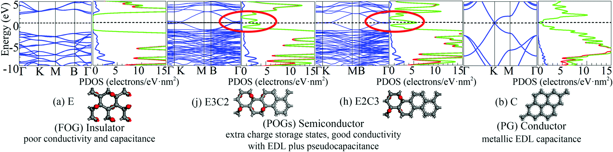 | ||
| Fig. 1 Representative energy band structures and density of states as well as the corresponding species: (a) fully oxidised graphene (FOG), (b) pure graphene (PG) and partially oxidised graphenes (POGs), corresponding to Fig. S3 (j and h) in the ESI.† In the middle, the dashed horizontal line denotes the Fermi level. In the DOS diagrams, the blue line denotes the s-orbital, red line the p-orbital and green line the sum. | ||
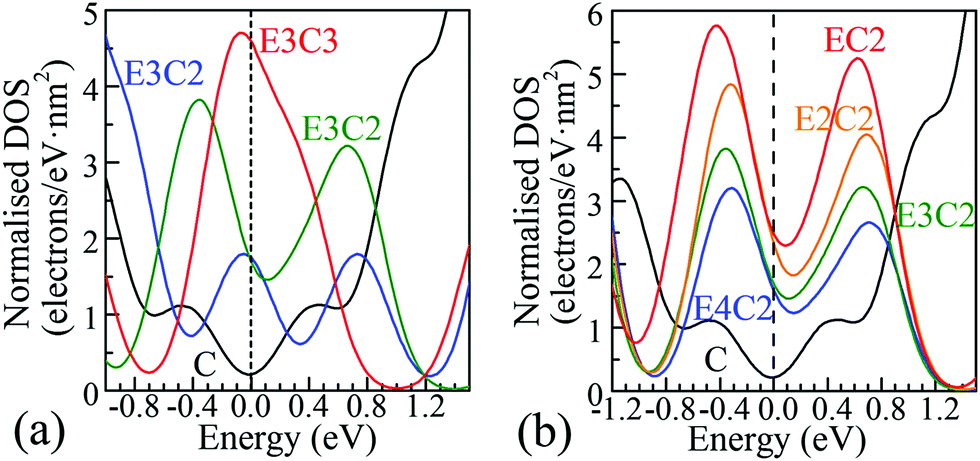 | ||
| Fig. 2 Representative DOS of POG species selected from Fig. S3 in the ESI† and magnified regions (with 90° anticlockwise rotation) around the Fermi level. The Fermi level corresponds to the black dashed vertical line at 0.0 eV. The solid black C curves in both figures show the DOS of PG around the Fermi level. (a) The columns of epoxy covered area were fixed to 3, the degree of ED goes up from E3C to E3C3; (b) the columns of π-conjugated double-bond carbon chains were fixed to 2. A smearing integration method in CASTEP with a width of 0.2 eV was used to obtain these DOS diagrams. | ||
| Class | Abb. form | UC area (Å2) | E g (eV) | Widtha (eV) | DOS max.b | Predicted propertyc |
|---|---|---|---|---|---|---|
| a These values of energy width were obtained from Fig. 2, corresponding to the range between the first valleys after the peak towards negative and positive energy respectively. b Sample from as-concerned energy level range within the width around the Fermi level. The DOS maximum was normalised against the area projected in the direction of c-axis of each unit cell, see the third column, therefore in a unit of electrons per eV nm2. c I: insulator; S: semiconductor; S-M: semi-metal; M: metal. | ||||||
| FOG | E | 21.05 | 4.286 | NA | 0.0 | I |
| POG | EC | 21.05 | 0.496 | 1.6 | 3.3 | S |
| EC2 | 63.15 | 0.041 | 2.4 | 3.2 | S-M | |
| EC3 | 42.10 | 0.289 | 1.9 | 5.4 | S | |
| E2C | 63.15 | 0.429 | 1.5 | 2.5 | S | |
| E2C2 | 42.10 | 0.182 | 2.3 | 4.8 | S | |
| E2C3 | 105.26 | 0.000 | 1.7 | 5.6 | S-M | |
| E3C | 42.10 | 0.666 | 1.6 | 1.8 | S | |
| E3C2 | 105.26 | 0.145 | 2.3 | 3.8 | S | |
| E3C3 | 63.15 | 0.027 | 1.7 | 4.7 | S-M | |
| E4C | 105.26 | 0.513 | 1.6 | 1.5 | S | |
| E4C2 | 63.15 | 0.227 | 2.3 | 3.2 | S | |
| E4C3 | 147.41 | 0.011 | 1.7 | 4.1 | S-M | |
| PG | C | 5.28 | 0.000 | 1.2 | 1.1 | M |
On one hand, the fully delocalised electrons endow PG with behaviour like that of the ordinary metal electrode offering typical electrical double layer (EDL) capacitance.
However, the ideal specific area of PG is 2630 m2 g−1, corresponding to the mass specific EDL capacitance of 526 F g−1.6 This means that the maximum charge density accumulated on the graphene sheet would be no more than 20 μC cm−2 in a 1 V cell. However, on the other hand, as can be seen in the Fig. 1(b), the DOS of PG decreases very quickly to almost zero when it approaches the Fermi level (or the Dirac cone).7 Such a low DOS around the common stability range of aqueous electrolyte further reduces the actual capacitance of PG because of the vanished quantum capacitance near the Fermi level.8 For FOG, a wide forbidden gap blocks all current flowing through the fully localised framework. Therefore, only negligible capacitance due to polarisation as in a conventional dielectric material could be observed in FOGs.
Completely different landscapes showed up in the case of POGs. Two approaches were adopted in this study to examine the impact of various electron delocalisation areas (EDAs) on the electronic structure. The first is to gradually increase the size of the π-conjugated column, denoted in Table 1 by C with a fixed number of epoxy groups denoted by E. The second is to maintain the size of the π-conjugated column with gradually increased areas of epoxy groups. Two selected electronic diagrams of POGs are shown in Fig. 1. The other results are collected in Fig. S3, ESI.† Intriguingly, a bunch of extra energy states can be observed near the Fermi level in energy bands and DOS diagram of all POGs within the range of ±3 eV. These extra states gain density and become more compact, as the EDA increases in the order of E3C, E3C2 and E3C3. However, when the EDA is fixed, the DOS maximum of each of these extra states decreases with the extension of the coverage of epoxy groups in the order of EC2, E2C2, E3C2 to E4C2. In Fig. 2, PG only has a very low value of DOS especially around the Fermi level. However quite a large increase in the DOS around this area showed in all POGs. Based on the normalised DOS curves, in some energy range, the charge capacity of these states can achieve 5–6 electrons per eV nm2, corresponding to 5 to 6 folds of that of PG (∼1.1 electrons per eV nm2).
Conclusive experimental revelation of the energy band structure and DOS in GO or POG is hampered by their complicated atomic configurations, but a few experimental results had offered some hope. A capacitive photocurrent spectroscopy technique was utilised to determine the electronic DOS for GOs and partially reduced GOs.9 DOS diagrams were extracted from the capacitive photocurrent spectra, and showed a series of extra states. Three discrete transition states at about 0.7, 1.6 and 3.2 eV found in ref. 9 were also observable in our DOS results of POGs, which are approximately aligned with those extra energy levels around the Fermi level in our study. Further, more additional states arise close to the Fermi level and become closer in energy space as the GO is reduced to a greater extent, again supporting our theoretical predictions.
Fig. 3 further shows the variation of Eg as a function of the sizes of EDA and epoxy group columns. As the epoxy group column is fixed in Fig. 3(a), Eg decreases with the expansion of the EDA. The exception is EC3 with an Eg value of 0.289 eV which is wider than those of the other three models. From Fig. 3(b), it is hard to summarise a clear Eg trend of the effect from increasing the epoxy group areas (EPAs) as the EDA is fixed, for the fluctuating data. Here, one may consider that increasing the EPA represents different distances between neighbouring EDAs. Hence the variation of EDA may play a greater influence on the electronic structure and Eg than that from the EPAs.
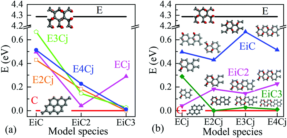 | ||
| Fig. 3 Effects of EDA and EPA on the energy band gap, Eg, of different POGs: (a) width of EDA, (b) size of EPA. Red and black horizontal lines represent PG with a band gap of 0 eV and FOG with a band gap of 4.286 eV, respectively. | ||
It is worth highlighting that different from previous studies, our view is that the influence arises mainly from the variation of EDAs rather than the defects or functional groups. This is because these extra energy states originate from delocalised electrons in regions of limited sizes, rather than from localised electrons in the epoxy groups, which can be verified through the projected DOS (PDOS) analysis, as shown in Fig. 4. It can be seen that carbons in the sp2 region with partial electron delocalisation are responsible for the main portion of population densities of those extra states, especially the p-orbitals. However, the sp3 carbons and oxygens whose electrons are fully localised contribute only a negligible portion. Therefore, it is rational to assign these extra states to the delocalised electrons, rather than the localised ones. Since these extra states are near the Fermi level, they should play a key role in charge storage over a wide range of energy levels or potentials, which is in line with pseudocapacitance.
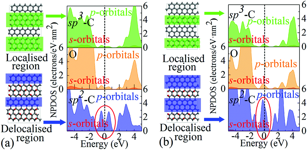 | ||
| Fig. 4 Normalised PDOS (NPDOS) analyses of two representative POG models: (a) E3C2 and (b) E2C3. The carbon atoms enclosed in the blue and green rectangles contain delocalised and localised electrons, respectively. | ||
In practice, partially reduced or oxidised GOs have been found to possess not only good EDL capacitance but also appreciable pseudocapacitance, thus have been proposed as a class of electrode materials with a great potential for supercapacitor applications.9 Since the actual oxidation and reduction processes are highly non-uniform, a large number of partially reduced or oxidised GO species, or more accurately GO fragments with a wide distribution of oxidation degrees, are formed in the same batch of samples under the identical or comparable experimental conditions.4 Apparently, these species have different degrees of ED.9c According to our theoretical calculations, discrete energy states near EF with a narrow Eg of the order of a few hundred meV (0.0–0.666 eV) emerge in the electronic band structure of POGs with different degrees of ED. More significantly, as shown in Fig. 2, these extra electronic states just reside in the region of the stable range of aqueous electrolyte and the scanning potential window of carbon-based supercapacitors. The distribution of width varies with different degrees of ED. For using POGs as electrode materials in supercapacitor, these new discrete states near the EF level can act as a series of charge storage states spreading over a sufficiently wide potential window to accept (or donate) electrons and therefore improve the Faradaic redox reactivity of PGOs, resulting in a boost of the pseudocapacitance in these species.
It is believed that, firstly, the distribution of these extra charge storage states decides the limits of the potential scanning window in which the behaviour of pseudocapacitance can be observed in the electrode material. As can be found in Fig. 2, all the charge storage states of POGs fall in an energy range wider than 2.0 eV, which compares well with the experimentally observed potential range of carbon materials in neutral aqueous electrolytes. Thus, charges can be injected into or extracted from these energy levels within the common range of the operating voltage of supercapacitors. Secondly, the population densities of these special states also decide the charge capacity in manners of pseudocapacitance of the electrode material. Here, it must be highlighted that this kind of charge storage is totally different from that in a traditional EDLC electrode as well as in a battery electrode that can be explained by the Nernst equation with one or several couples of Faradaic redox peaks on the CVs. These extra energy states can distribute in a wide range of energy levels caused by different degrees of ED, hence obligate space to store charges in a quasi-continuous potential window. Also, these intensive energy states around the Fermi level can also improve the redox activity of POGs resulting in specific adsorption of ions, which has also been observed and proven in many studies on the catalytic activity of POGs. In addition, this mechanism also corresponds to a fast reversible Faradaic process intrinsically with improved redox activities by a partial charge transfer between partially reduced or oxidised GOs and electrolyte ions through the ‘bridge’ of extra energy states. These discrete energy states can also be taken into account in probable states to accommodate electrons or holes, leading to greater excess charges over and above the charge stored within the ubiquitous EDL. Meanwhile, to some extent, the reserved good conductivity, such as charge mobility along the zigzag chain of π-conjugated double bond, allows charges (electrons or holes) to flow in and out efficiently. Accordingly, this mechanism is thought as another new possible contribution to the pseudocapacitance of the POG based electrode materials.
Detailed electronic structures of a series of simple but new models of GOs with various coverage areas of epoxy groups and ED zones have been calculated and investigated by the DFT method. A tuneable Eg value ranging from 0 eV to 0.666 eV has been observed, depending on model structures. Extra energy states close to the EF level have been identified only in all the studied PGOs but not in PG and FOG. This finding may not be surprising or unexpected, but it is not yet reported in the literature. The results have also indicated a stronger correlation of the DOS maximum with the sizes of the ED zones, instead of that covered by the epoxy groups. These findings predict transfer of partially delocalised electrons over a wide range of potentials. Such behaviour is in line with the experimentally observed pseudocapacitance, but contradicts that governed by the feature potential of the Nernst's Law for the transfer of localised valence electrons.
In principle, the charge storage mechanism proposed in this work should be applicable to other pseudocapacitive materials, e.g. transition metal oxides (TMOs) and electronically conducting polymers (ECPs) which all have states of delocalised electrons. In the RuO2 lattice, delocalised states originate from the overlapped d-orbitals of Ru atoms and the p-orbitals of O atoms.10a In α-MnO2, insertion ions introduced charge-switching states within the band gap are responsible for the pseudocapacitance.10b For ECPs, the conjugated bonds are responsible for electron delocalisation. We believe that to enable pseudocapacitance (or redox activity), electron delocalisation should be confined, at least partially, in suitable special dimensions, such as the nano-structures in TMOs and the limited lengths of the conjugated bonds in ECPs. It is our hope that this communication can form the basis for future studies in the related fields in terms of theoretical analysis, particularly via modelling, and experimental demonstration.
This work was supported by the Engineering and Physical Sciences Research Council [grant numbers EP/J000582/1, GR/R68078], Aviation Industry Corporation of China, China Scholarship Council (JFL), and Ningbo Municipal Government (3315 Plan, 2014A35001-1).
Conflicts of interest
There are no conflicts to declare.Notes and references
- (a) Z. Lin, Y. Liu, Y. Yao, O. J. Hildreth, Z. Li, K. Moon and C.-P. Wong, J. Phys. Chem. C, 2011, 115, 7120–7125 CrossRef CAS; (b) F. Liu and D. Xue, Chem. – Eur. J., 2013, 19, 10716–10722 CrossRef CAS PubMed; (c) Y. Zhu, S. Murali, M. D. Stoller, K. J. Ganesh, W. Cai, P. J. Ferreira, A. Pirkle, R. M. Wallace, K. A. Cychosz, M. Thommes, D. Su, E. A. Stach and R. S. Ruoff, Science, 2011, 332, 1537–1541 CrossRef CAS PubMed; (d) T. Lin, I.-W. Chen, F. Liu, C. Yang, H. Bi, F. Xu and F. Huang, Science, 2015, 350, 1508–1513 CrossRef CAS PubMed.
- (a) C. Xu, B. Xu, Y. Gu, Z. Xiong, J. Sun and X. S. Zhao, Energy Environ. Sci., 2013, 6, 1388–1414 RSC; (b) A. Lerf, H. He, M. Forster and J. Klinowski, J. Phys. Chem. B, 1998, 102, 4477–4482 CrossRef CAS.
- (a) G. Z. Chen, Prog. Nat. Sci., 2013, 23, 245–255 CrossRef; (b) S. W. Zhang and G. Z. Chen, Energy Mater., 2008, 3, 186–200 CrossRef CAS; (c) G. Z. Chen, Int. Mater. Rev., 2017, 62, 173–202 CrossRef CAS.
- S. J. Clark, M. D. Segall, C. J. Pickard, P. J. Hasnip, M. J. Probert, K. Refson and M. C. Payn, Z. Kristallogr. – Cryst. Mater., 2005, 220, 567–570 CAS.
- A. H. Castro Neto, F. Guinea, N. M. R. Peres, K. S. Novoselov and A. K. Geim, Rev. Mod. Phys., 2009, 81, 109–162 CrossRef CAS.
- M. Pumera, Chem. Rec., 2009, 9, 211–223 CrossRef CAS PubMed.
- B. C. Wood, T. Ogitsu, M. Otani and J. Biener, J. Phys. Chem. C, 2014, 118, 4–15 CAS.
- (a) M. Mousavi-Khoshdel, E. Targholi and M. J. Momeni, J. Phys. Chem. C, 2015, 119, 26290–26295 CrossRef CAS; (b) T. Bansal, A. D. Mohite, H. M. Shah, C. Galande, A. Srivastava, J. B. Jasinski, P. M. Ajayan and B. W. Alphenaar, Carbon, 2012, 50, 808–814 CrossRef CAS; (c) B. W. Alphenaar, T. Bansal, A. D. Mohite, H. M. Shah, C. Galande, A. Srivastava, J. B. Jasinski and P. M. Ajayan, ECS Trans., 2012, 45, 31–39 CrossRef CAS.
- (a) B. Rajagopalan and J. Chung, Nanoscale Res. Lett., 2014, 9, 535 CrossRef PubMed; (b) J. Yang and S. Gunasekaran, Carbon, 2013, 51, 36–544 CrossRef CAS; (c) K. Erickson, R. Erni, Z. Lee, N. Alem, W. Gannett and A. Zettl, Adv. Mater., 2010, 22, 4467–4472 CrossRef CAS PubMed.
- (a) V. Ozoliņš, F. Zhou and M. Asta, Acc. Chem. Res., 2013, 46, 1084–1093 CrossRef PubMed; (b) M. J. Young, A. M. Holder, S. M. George and C. B. Musgrave, Chem. Mater., 2015, 27, 1172–1180 CrossRef CAS.
Footnote |
| † Electronic supplementary information (ESI) available: The detailed structure parameters of each GOs models and pure graphene after geometry optimisation. See DOI: 10.1039/c7cc04344a |
| This journal is © The Royal Society of Chemistry 2017 |