
 Open Access Article
 This Open Access Article is licensed under a
 Creative Commons Attribution 3.0 Unported Licence
An annealing-free aqueous-processed anatase TiO2 compact layer for efficient planar heterojunction perovskite solar cells†
Chengwu
Yang
a,
Mingyu
Yu
a,
Dichun
Chen
b,
Yaqing
Zhou
a,
Wei
Wang
a,
Yang
Li
a,
Tung-Chun
Lee
 *c and
Daqin
Yun
*a
*c and
Daqin
Yun
*a
aCollege of Energy, Xiamen University, Xiamen 361002, China. E-mail: dqyun@xmu.edu.cn
bXiamen Branch of Luoyang Ship Material Research Institute, Xiamen, 361006, China
cDepartment of Chemistry and Institute for Materials Discovery, University College London (UCL), UK. E-mail: tungchun.lee@ucl.ac.uk
First published on 13th June 2017
Abstract
A facile aqueous-based fabrication scheme is developed for producing annealing-free anatase TiO2 (AF-TiO2) films that exhibit efficient electron transport properties in planar heterojunction perovskite solar cells (PSCs). AF-TiO2 films are fabricated by spin coating on a substrate a colloidal solution of anatase TiO2 nanoparticles (NPs) prepared via a low temperature hydrolytic sol–gel method. The resultant AF-TiO2 films show low electrical resistance, high transmittance in the visible and near-infrared regions and facilitation of high-quality perovskite film formation, which can be attributed to their homogeneous surface morphology and nanocrystallinity. The AF-TiO2 based PSCs achieve a power conversion efficiency (PCE) of 18.29 ± 0.18%, showing significant improvement compared to the control PSCs (PCE = 11.33 ± 0.32%) based on TiO2 films made by high-temperature annealing of amorphous TiO2 (HTA-TiO2).
Solution-processable perovskite solar cells (PSCs) have recently attracted significant attention as a promising candidate for making high efficiency and flexible photovoltaic devices.1–6 To date, numerous PSCs using TiO2 mesoporous structures have been shown to exhibit high power conversion efficiencies (PCEs) of over 20%.7–10 However, mesoporous TiO2 layers require a high-temperature annealing process (over 450 °C), which limits their use in flexible PSCs. As an alternative to mesoporous TiO2 PSCs, planar heterojunction (PHJ) PSCs made via low-temperature (<150 °C) processing have been investigated extensively due to their simple device structures and their compatibility with flexible polymeric substrates as well as inverted device designs.11–14 In general, the p–i–n type PHJ PSC structure consists of an electron transport layer (ETL), a perovskite absorber layer and a hole transport layer (HTL). The ETL and HTL are responsible for extracting photo-generated charge carriers from the perovskite layer and transporting these carriers to the designated electrodes. Various types of materials have been employed in carrier transport layers, such as PEDOT:PSS, NiOx, CuSCN, poly(triaryl amine) (PTAA) and 2,2′,7,7′-tetrakis-(N,N-di-p-methoxyphenylamine)-9,9′-spirobifluorene (Spiro-OMeTAD) as hole transport layers, and ZnO, SnO2, CsCO3, PCBM and TiO2 as electron transport layers.7,15–21 Among these ETLs, TiO2 is considered to be a promising electron transport material because of its environmentally friendly nature, wide band gap, high electron mobility and good stability.22–24
Recently, several vacuum deposition approaches have been developed for fabricating low-temperature processable TiO2 ETLs for PHJ PSCs, such as atomic layer deposition,25 electron-beam evaporation,26 and magnetron sputtering.14 Compared to vacuum methods, however, solution-based techniques are generally more cost-effective and scalable. Among them, sol–gel methods are arguably the most widely adopted routes for depositing TiO2 films owing to ease in fabrication and low cost.4,11,27–29 Nevertheless, the as-prepared TiO2 films via the sol–gel methods are generally amorphous and therefore exhibit poor electrical conductivity, which incurs negative impacts on the performance of PSCs.11,30 Strategies have been developed to enhance the electrical properties of TiO2 films via optimising their morphology, doping and composition; these strategies include surface modification of TiO2 with TiCl4 treatment, ozone (O3) treatment,31,32 and doping modification of the TiO2 film with an appropriate substitution of Li+, Mg2+, Al3+, Y3+, and Nb5+.4,18,33–35 In particular, the formation of crystalline TiO2 at a low temperature is considered to be one of the most direct and efficient strategies to improve the electrical characteristics for highly efficient PSCs.29,30 In this context, considerable effort has been devoted to prepare TiO2 nanocrystals (NCs) through a low-temperature non-hydrolytic sol–gel method for PSC applications.16,32,36 However, it remains a challenge to synthesise high-quality anatase TiO2 NCs via the low-temperature hydrolytic sol–gel method for efficient PSCs.
Herein, we report a facile, efficient and environmentally friendly approach for preparing ultrathin anatase TiO2 films via an aqueous-based and annealing-free fabrication scheme. The resultant annealing-free anatase TiO2 (AF-TiO2) films can act as an efficient electron transport layer for planar heterojunction PSCs. The nanocrystalline anatase TiO2 nanoparticles (NPs) prepared by this low-temperature hydrolytic sol–gel method can form stable nanocolloidal solutions in aqueous media, enabling the preparation of a smooth film with high optical transmittance. The resultant AF-TiO2 film shows better electron extraction ability than that of the conventional TiO2 films prepared in organic solvents and treated via high-temperature annealing processes, abbreviated as HTA-TiO2 below. Moreover, the AF-TiO2 compact layer was also found to facilitate the formation of high-quality perovskite films.
A general drawback of the hydrolytic sol–gel method is the amorphous nature of the resultant TiO2 NPs and thus the requirement of a post-synthetic high-temperature (over 450 °C) annealing step to induce crystallisation. In our case, the low-temperature hydrolysis of titanium(IV) isopropoxide (TTIP) is performed via a sol–gel method in the presence of HNO3 as the hydrolysing agent, resulting in the formation of nanocrystalline anatase TiO2 NPs (see the ESI† for detailed experimental procedures), consistent with other similar systems in the literature.37 In this method, the fast initial nucleation step induces the formation of small electrostatically stabilised TiO2 NPs. The subsequent ageing step at 80 °C triggers the formation of small nanocrystalline anatase domains within a TiO2 NP. The mild reaction conditions (80 °C, 1 atmosphere pressure) and surfactant-free aqueous solvent systems make this method a promising way to produce high-quality anatase TiO2 NPs for PSCs and other applications.
The as-synthesised anatase TiO2 NPs can be readily dispersed in water to form nanocolloidal solutions that are stable for months (inset of Fig. 1a; concentration = 20 mg mL−1). Powder X-ray diffraction (XRD) measurements of this sample reveal typical diffraction peaks of anatase TiO2 (Fig. 1a). In particular, the diffraction peaks centred at 25.40°, 38.28°, 47.46°, 54.26°, and 62.68° were assigned to (101), (004), (200), (105) and (204) diffractions, respectively. This result verifies that the as-synthesised TiO2 NPs indeed contain a significant amount of the anatase domains. Scherrer peak width analysis22 reveals the average size of the nanocrystalline domains to be approximately 6.1 nm. The inset of Fig. 1b shows a top-view scanning electron microscopy (SEM) image of an AF-TiO2 film on a glass/ITO substrate prepared by spin coating. It was observed that AF-TiO2 can form a dense, pinhole-free, and uniform continuous film compared to that of HTA-TiO2 (ESI,† Fig. S1). Additionally, the resultant AF-TiO2 film shows good optical transparency, with transmittance greater than 85% in the entire visible region (Fig. 1b). For comparison, the effects of anatase TiO2 film thicknesses on transmittance performance are shown in Fig. S2 (ESI†).
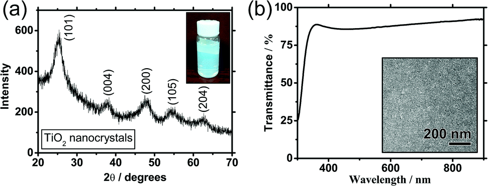 | ||
| Fig. 1 (a) Powder X-ray diffraction pattern of AF-TiO2 nanoparticles. Diffraction peaks of each crystal plane are labelled. (b) Transmittance spectra of AF-TiO2 films deposited on a glass substrate. The inset shows a representative SEM image of AF-TiO2 deposited on a glass/ITO substrate, exhibiting a smooth morphology. | ||
To gain further insights into the nanoscale morphology and nanocrystal structures, high-resolution transmission electron microscopy (HRTEM) has been performed. The HRTEM image (Fig. 2a) reveals that the TiO2 NPs are around 15–25 nm in diameter. By analysing the diffraction-contrast image and the fast-Fourier transform FFT images of selected areas, individual crystal domains within a single NP are identified to have a domain size of 2.5–5.5 nm (Fig. 2b and c), consistent with that obtained by Scherrer peak width analysis. The selected area electron diffraction (SAED) pattern (Fig. 2a, inset) displayed typical electron diffraction rings corresponding to the (101), (004), (200), and (105) lattice planes of the anatase structure of TiO2, consistent with the powder XRD results (Fig. 1a). These results indicate that the TiO2 NPs indeed contain a high proportion of nanocrystalline anatase phase, implying that they have a reduced number of surface defect traps and could therefore enhance charge extraction on the interface between the TiO2 layer and the perovskite layer.
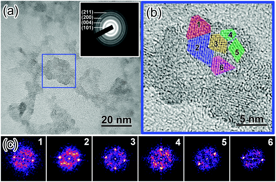 | ||
| Fig. 2 (a) Bright-field HRTEM image of TiO2 nanocrystals deposited on a carbon film. The inset shows a selected area electron diffraction of TiO2 NPs. Diffraction rings of the (101), (004), (200) and (105) planes are observed. (b) Zoom-in of the region of interest denoted by the blue square in (a). Selected adjacent nanocrystal domains are highlighted and numbered. Domain size: 2.5–5.5 nm. (c) FFT images of selected nanocrystal domains in (b), verifying the difference in crystal orientation. | ||
To investigate the performance of the AF-TiO2 films as ETLs in PHJ PSCs, a complete PSC device has been fabricated. A cross-sectional SEM image of a typical device architecture is shown in Fig. 3a. The electrodes of indium tin oxide (ITO) and Ag were used as the bottom cathode and the top anode, respectively. The thicknesses of the ETL (TiO2), the HTL (Spiro-OMeTAD) and the (FAPbI3)x(MAPbCl3)1−x perovskite absorber layer are approximately 60 nm, 260 nm, and 600 nm, respectively. It is noted that the smooth morphology of the AF-TiO2 films can facilitate the formation of highly crystalline and compact perovskite films (see Fig. S1, S3–S5, ESI† for details).
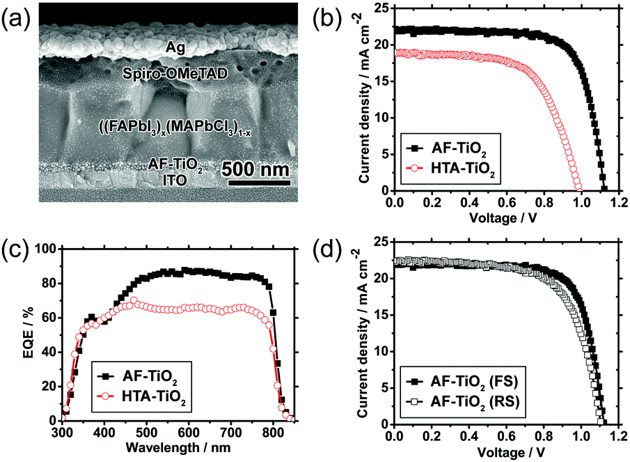 | ||
| Fig. 3 (a) Cross-sectional SEM image of a completed PSC device, with the structure of glass/ITO/TiO2/(FAPbI3)x (MAPbCl3)1−x/Spiro-OMeTAD/Ag. (b) J–V curves of typical devices using AF-TiO2 and HTA-TiO2 as ETLs. The measurements were performed under simulated AM 1.5 G sunlight (100 mW cm−2). (c) EQE spectra of representative devices comprising AF-TiO2 and HTA-TiO2 as ETLs. (d) Forward-scan (from 0 V to 1.2 V) and reverse-scan (from 1.2 V to 0 V) J–V curves of a typical AF-TiO2 based device. | ||
Fig. 3b shows the current–density–voltage (J–V) curves of the perovskite solar cells based on AF-TiO2 compared to devices made of HTA-TiO2. The photovoltaic parameters of the devices are summarised in Table 1. Data in Table 1 show that the solar cell of HTA-TiO2 exhibits considerably low short-circuit current density (Jsc), open-circuit voltage (Voc), and fill factor (FF) values. In contrast, the overall PCE, including Jsc, Voc, and FF, significantly increased when AF-TiO2 NPs were used as the ETL. We propose that the notably high PCE of PSCs based on the AF-TiO2 ETL is caused by the high content of the nanocrystalline anatase phase within the compact layer and the highly homogeneous morphology, which together favour electron extraction by reducing the rate of carrier recombination, compared to that of HTA-TiO2.11,21,32 In particular, the dramatic difference in series resistance (Rs) could be attributed to the presence of nanocrystalline TiO2 domains that enhance electron transport, thereby improving the electrical characteristics.22 As a result, the devices of AF-TiO2 exhibit a Jsc of 22.27 ± 0.19 mA cm−1, a Voc of 1.11 ± 0.01, and a FF of 73.63 ± 0.86%, corresponding to a PCE of 18.29 ± 0.18%, which shows significant improvement compared to that of control PSCs (PCE = 11.33 ± 0.32%) using HTA-TiO2 films as the ETL. This result demonstrates that planar structure photovoltaic devices based on AF-TiO2 can indeed achieve a highly efficient power conversion, which sheds light on the development of highly efficient and flexible PSCs without relying on mesoporous TiO2 structures.
| Compact layer (Annealing temperature) | Thicknessa (nm) | J sc (mA cm−2) | V oc (V) | FF (%) | PCE (%) | R S (Ω cm2) | |
|---|---|---|---|---|---|---|---|
| a Thickness of the TiO2 films was measured using a surface profilometer, consistent with the thickness determined by SEM. | |||||||
| AF-TiO2 (25 °C) | 58 ± 2 | Champion | 22.41 | 1.10 | 74.87 | 18.50 | 4.49 |
| Average | 22.27 ± 0.19 | 1.11 ± 0.01 | 73.63 ± 0.86 | 18.29 ± 0.18 | 4.79 ± 0.20 | ||
| HTA-TiO2 (500 °C) | 61 ± 2 | Champion | 18.85 | 0.99 | 62.74 | 11.70 | 11.38 |
| Average | 18.75 ± 0.11 | 0.98 ± 0.01 | 61.47 ± 1.44 | 11.33 ± 0.32 | 12.56 ± 1.34 | ||
Typical external quantum efficiency (EQE) data of the devices are shown in Fig. 3c. The integrated Jsc values of the devices calculated from the EQE data were 21.63 mA cm−2 and 17.45 mA cm−2 for AF-TiO2 and HTA-TiO2, respectively, which match well with the J–V measurement data (Table 1). The enhancement of EQE from 500 nm to 800 nm can be attributed to the smaller Rs value and the improved morphology and crystallisation of the perovskite film facilitated by the AF-TiO2 ETL (Fig. S1, S3–S5, ESI†).
The J–V curves and parameters of the AF-TiO2 device measured for reverse and forward scan directions are shown in Fig. 3d and Table S2 (ESI†). Notably, the device does not exhibit distinct hysteresis, which is an indicator of inefficient charge transfer at the TiO2/perovskite interface, ferroelectric effects, ionic displacement and the trapping/detrapping of the charge carrier at the perovskite interface.38–41 In an attempt to optimise the performance of TiO2 ETLs, we have investigated the effects of the ETL thickness and that of the additional low-temperature annealing step after the deposition of anatase TiO2 NPs by spin coating. Device-level measurement data based on 10 PSCs per configuration are presented in the ESI† (Fig. S2, S6–S12 and Tables S1–S4).
Electrical impedance spectroscopy (EIS) was performed to further study the interfacial charge transport properties of the PSCs.14,42 Nyquist plots of the devices were measured at a DC bias of 0–0.8 V in the dark and the equivalent circuit model for the perovskite solar cells is shown in Fig. 4a (see Fig. S12 (ESI†) for details). Compared to HTA-TiO2-based devices, the AF-TiO2 based devices exhibit significantly smaller Rs and larger recombination resistance (Rrec), indicating more efficient extraction and transport of electrons at the AF-TiO2/perovskite interface, thus resulting in larger Jsc, Voc and FF values for these solar cells.
 | ||
| Fig. 4 (a) Nyquist plots of PSCs based on AF-TiO2 and HTA-TiO2 in the dark at a DC bias of 0 V. A 20 mV AC signal was applied with a frequency range of 0.01 Hz to 100 kHz. The inset shows the equivalent circuit adopted. (b) Nyquist plots of the high frequency region. (c) Rs as a function of bias. (d) Rrec as a function of bias. | ||
In conclusion, we have developed a facile and environmentally friendly method for fabricating nanocrystalline anatase TiO2 films as compact electron transport layers for PHJ PSCs. TiO2 NPs with small (2.5–5.5 nm) anatase domains were successfully prepared via a low temperature hydrolytic sol–gel method. The aqueous TiO2 nanocolloids can form via spin coating continuous thin films that show superior electron extraction capability and high optical transmittance and can facilitate the formation of high-quality perovskite films. The PSC based on AF-TiO2 achieves a PCE of 18.29 ± 0.18%. This powerful and generic strategy offers a novel way towards green, efficient and flexible PSC designs and beyond.
The research was funded by the Fundamental Research Funds for the Central Universities (2013121031) and the UCL BEAMS Future Leader Award through the EPSRC 2016 Institutional Sponsorship Award (EP/P511262/1). DY is grateful to the China Scholarship Council for funding. Nanfeng Zheng is acknowledged for his assistance in the IPCE measurements. Suyuan Xie is also gratefully acknowledged for his assistance in the J–V characteristic measurements.
Notes and references
- A. Kojima, K. Teshima, Y. Shirai and T. Miyasaka, J. Am. Chem. Soc., 2009, 131, 6050–6051 CrossRef CAS PubMed.
- M. M. Lee, J. Teuscher, T. Miyasaka, T. N. Murakami and H. J. Snaith, Science, 2012, 338, 643–647 CrossRef CAS PubMed.
- J. Burschka, N. Pellet, S. J. Moon, R. Humphry-Baker, P. Gao, M. K. Nazeeruddin and M. Gratzel, Nature, 2013, 499, 316–319 CrossRef CAS PubMed.
- H. Zhou, Q. Chen, G. Li, S. Luo, T. B. Song, H. S. Duan, Z. Hong, J. You, Y. Liu and Y. Yang, Science, 2014, 345, 542–546 CrossRef CAS PubMed.
- G. E. Eperon, S. D. Stranks, C. Menelaou, M. B. Johnston, L. M. Herz and H. J. Snaith, Energy Environ. Sci., 2014, 7, 982 CAS.
- N. J. Jeon, J. H. Noh, W. S. Yang, Y. C. Kim, S. Ryu, J. Seo and S. I. Seok, Nature, 2015, 517, 476–480 CrossRef CAS PubMed.
- W. S. Yang, J. H. Noh, N. J. Jeon, Y. C. Kim, S. Ryu, J. Seo and S. I. Seok, Science, 2015, 348, 1234–1237 CrossRef CAS PubMed.
- D. Bi, W. Tress, M. I. Dar, P. Gao, J. Luo, C. Renevier, K. Schenk, A. Abate, F. Giordano and J.-P. C. Baena, Sci. Adv., 2016, 2, 1501170 Search PubMed.
- X. Li, D. Bi, C. Yi, J.-D. Décoppet, J. Luo, S. M. Zakeeruddin, A. Hagfeldt and M. Grätzel, Science, 2016, 353, 58–62 CrossRef CAS PubMed.
- D. Bi, C. Yi, J. Luo, J.-D. Décoppet, F. Zhang, S. M. Zakeeruddin, X. Li, A. Hagfeldt and M. Grätzel, Nat. Energy, 2016, 1, 16142 CrossRef CAS.
- B. Conings, L. Baeten, T. Jacobs, R. Dera, J. D'Haen, J. Manca and H. G. Boyen, APL Mater., 2014, 2, 081505 CrossRef.
- C.-H. Chiang, Z.-L. Tseng and C.-G. Wu, J. Mater. Chem. A, 2014, 2, 15897–15903 CAS.
- Y. Li, L. Meng, Y. M. Yang, G. Xu, Z. Hong, Q. Chen, J. You, G. Li, Y. Yang and Y. Li, Nat. Commun., 2016, 7, 10214 CrossRef CAS PubMed.
- D. Yang, R. Yang, J. Zhang, Z. Yang, S. Liu and C. Li, Energy Environ. Sci., 2015, 8, 3208–3214 CAS.
- D. Liu and T. L. Kelly, Nat. Photonics, 2013, 8, 133–138 CrossRef.
- H.-H. Wang, Q. Chen, H. Zhou, L. Song, Z. S. Louis, N. D. Marco, Y. Fang, P. Sun, T.-B. Song, H. Chen and Y. Yang, J. Mater. Chem. A, 2015, 3, 9108–9115 CAS.
- S. Ye, W. Sun, Y. Li, W. Yan, H. Peng, Z. Bian, Z. Liu and C. Huang, Nano Lett., 2015, 15, 3723–3728 CrossRef CAS PubMed.
- W. Chen, Y. Wu, Y. Yue, J. Liu, W. Zhang, X. Yang, H. Chen, E. Bi, I. Ashraful and M. Grätzel, Science, 2015, 350, 944–948 CrossRef CAS PubMed.
- D. P. McMeekin, G. Sadoughi, W. Rehman, G. E. Eperon, M. Saliba, M. T. Hörantner, A. Haghighirad, N. Sakai, L. Korte and B. Rech, Science, 2016, 351, 151–155 CrossRef CAS PubMed.
- Y. Wu, X. Yang, W. Chen, Y. Yue, M. Cai, F. Xie, E. Bi, A. Islam and L. Han, Nat. Energy, 2016, 1, 16148 CrossRef CAS.
- Q. Jiang, L. Zhang, H. Wang, X. Yang, J. Meng, H. Liu, Z. Yin, J. Wu, X. Zhang and J. You, Nat. Energy, 2016, 2, 16177 CrossRef.
- K. Wojciechowski, M. Saliba, T. Leijtens, A. Abate and H. J. Snaith, Energy Environ. Sci., 2014, 7, 1142–1147 CAS.
- D. Li, Y. Chen, P. Du, Z. Zhao, H. Zhao, Y. Ma and Z. Sun, RSC Adv., 2015, 5, 88973–88978 RSC.
- Y. Zhao, Q. Zeng, X. Liu, S. Jiao, G. Pang, X. Du, K. Zhang and B. Yang, J. Mater. Chem. A, 2016, 4, 11738–11746 CAS.
- J. P. Correa Baena, L. Steier, W. Tress, M. Saliba, S. Neutzner, T. Matsui, F. Giordano, T. J. Jacobsson, A. R. Srimath Kandada, S. M. Zakeeruddin, A. Petrozza, A. Abate, M. K. Nazeeruddin, M. Grätzel and A. Hagfeldt, Energy Environ. Sci., 2015, 8, 2928–2934 CAS.
- Y. Li, J. K. Cooper, W. Liu, C. M. Sutter-Fella, M. Amani, J. W. Beeman, A. Javey, J. W. Ager, Y. Liu, F. M. Toma and I. D. Sharp, Nat. Commun., 2016, 7, 12446 CrossRef CAS PubMed.
- M. Grätzel, J. Sol-Gel Sci. Technol., 2001, 22, 7–13 CrossRef.
- L. Guo, C. Fei, R. Zhang, B. Li, T. Shen, J. Tian and G. Cao, Sci. China Mater., 2016, 59, 710–718 CrossRef.
- G. Yang, H. Tao, P. Qin, W. Ke and G. Fang, J. Mater. Chem. A, 2016, 4, 3970–3990 CAS.
- A. Yella, L. P. Heiniger, P. Gao, M. K. Nazeeruddin and M. Gratzel, Nano Lett., 2014, 14, 2591–2596 CrossRef CAS PubMed.
- I. Jeong, H. Jung, M. Park, J. S. Park, H. J. Son, J. Joo, J. Lee and M. J. Ko, Nano Energy, 2016, 28, 380–389 CrossRef CAS.
- Z. Liu, Q. Chen, Z. Hong, H. Zhou, X. Xu, N. De Marco, P. Sun, Z. Zhao, Y. B. Cheng and Y. Yang, ACS Appl. Mater. Interfaces, 2016, 8, 11076–11083 CAS.
- H. Zhang, J. Shi, X. Xu, L. Zhu, Y. Luo, D. Li and Q. Meng, J. Mater. Chem. A, 2016, 4, 15383–15389 CAS.
- Y. Bai, Q. Dong, Y. Shao, Y. Deng, Q. Wang, L. Shen, D. Wang, W. Wei and J. Huang, Nat. Commun., 2016, 7, 12806 CrossRef CAS PubMed.
- D. Liu, S. Li, P. Zhang, Y. Wang, R. Zhang, H. Sarvari, F. Wang, J. Wu, Z. Wang and Z. D. Chen, Nano Energy, 2017, 31, 462–468 CrossRef CAS.
- N. D. Marco, H. Zhou, Q. Chen, P. Sun, Z. Liu, L. Meng, E.-P. Yao, Y. Liu, A. Schiffer and Y. Yang, Nano Lett., 2016, 16, 1009–1016 CrossRef CAS PubMed.
- G. Li, S. Zhang and J. Yu, J. Am. Ceram. Soc., 2011, 94, 4112–4115 CrossRef CAS.
- Y. Shao, Z. Xiao, C. Bi, Y. Yuan and J. Huang, Nat. Commun., 2014, 5, 5784 CrossRef CAS PubMed.
- W. Tress, N. Marinova, T. Moehl, S. Zakeeruddin, M. K. Nazeeruddin and M. Grätzel, Energy Environ. Sci., 2015, 8, 995–1004 CAS.
- J. Wei, Y. Zhao, H. Li, G. Li, J. Pan, D. Xu, Q. Zhao and D. Yu, J. Phys. Chem. Lett., 2014, 5, 3937–3945 CrossRef CAS PubMed.
- J. M. Frost, K. T. Butler and A. Walsh, APL Mater., 2014, 2, 081506 CrossRef.
- D. Liu, J. Yang and T. L. Kelly, J. Am. Chem. Soc., 2014, 136, 17116 CrossRef CAS PubMed.
Footnote |
| † Electronic supplementary information (ESI) available: Experimental details including synthesis, experimental procedure and supporting data. See DOI: 10.1039/c7cc01104k |
| This journal is © The Royal Society of Chemistry 2017 |