
 Open Access Article
 This Open Access Article is licensed under a Creative Commons Attribution-Non Commercial 3.0 Unported Licence
Anisotropic ultrahigh hole mobility in two-dimensional penta-SiC2 by strain-engineering: electronic structure and chemical bonding analysis
Yuanfeng Xua,
Zeyu Ninga,
Hao Zhang *ac,
Gang Nia,
Hezhu Shaob,
Bo Penga,
Xiangchao Zhanga,
Xiaoying Hea,
Yongyuan Zhuc and
Heyuan Zhua
*ac,
Gang Nia,
Hezhu Shaob,
Bo Penga,
Xiangchao Zhanga,
Xiaoying Hea,
Yongyuan Zhuc and
Heyuan Zhua
aDepartment of Optical Science and Engineering, Key Laboratory of Micro and Nano Photonic Structures (Ministry of Education), Fudan University, Shanghai 200433, China. E-mail: yuanfengxu15@fudan.edu.cn; zhangh@fudan.edu.cn
bNingbo Institute of Materials Technology and Engineering, Chinese Academy of Sciences, Ningbo 315201, China
cNanjing University, National Laboratory of Solid State Microstructure, Nanjing 210093, China
First published on 28th September 2017
Abstract
Monolayer pentagonal silicon dicarbide is a 2D material composed entirely of pentagons, and it possesses novel electronic properties possibly leading to many potential applications. In this paper, using first-principles calculations, we have systematically investigated the electronic, mechanical and transport properties of monolayer penta-SiC2 by strain-engineering. By applying in-plane tensile or compressive strain, it is possible to modulate the physical properties of monolayer penta-SiC2, which subsequently changes the transport behaviour of the carriers. More interestingly, at room temperature, the uniaxial compressive strain of −8% along the a-direction can enhance the hole mobility of monolayer penta-SiC2 along the b-direction by almost three orders of magnitude up to 1.14 × 106 cm2 V−1 s−1, which is much larger than that of graphene, while similar strains have little influence on the electron mobility. The ultrahigh and strain-modulated carrier mobility in monolayer penta-SiC2 may lead to many novel applications in high-performance electronic and optoelectronic devices.
1 Introduction
Two-dimensional (2D) materials have attracted great attention in the fields of nanoscale materials and nanotechnology since the experimental realization of graphene,1–3 which possesses remarkable mechanical, electronic and optical properties4–7 possibly leading to many novel applications in microelectronic and optoelectronic devices. A number of graphene-like layered structures with different chemical compositions and different crystal structures have been proposed and synthesised since then.8–10 Recently, Zhang et al.11 predicted a new 2D material composed entirely of carbon pentagons, i.e. penta-graphene, formed by the mixed sp2/sp3 orbital hybridization of C atoms, which was proven to be dynamically and mechanically stable, and can withstand temperatures as high as 1000 K.11 Monolayer penta-graphene possesses an unusual negative Poisson’s ratio, an ultrahigh ideal strength outperforming graphene and other interesting electronic properties,11,12 which make it a potential candidate for wide applications in optoelectronics and photovoltaics devices.Many efforts have been devoted to the discovery of new 2D materials with a penta structure since the successful prediction of penta-graphene.13,14 The silicon counterpart of the penta structure was proposed as well, although it is dynamically unstable in the monolayer form.15 Recently, a novel pentagonal structure composed of carbon and silicon atoms formed by sp2d hybridization, i.e. pentagonal silicon dicarbide (penta-SiC2), has been proposed and further confirmed to be dynamically stable and exhibits enhanced similar electronic properties compared to penta-graphene.16
However, during the processes of experimental realization of 2D materials like monolayer penta-SiC2, the mismatch between the 2D material and the substrate often results in the formation of crystal distortion due to strain or stress modulation, also called straintronics.17,18 Experimental results have shown that strains of up to 11% are possible for monolayer MoS2 in an AFM indentation experiment without bond breaking.19,20 Therefore it is necessary to investigate the strain-dependence properties of 2D materials with the purpose of comparison with experimental results. In addition, strain-engineering (external strain and stress) is an effective way to modulate the electronic, mechanical, optical and transport properties of 2D materials.21–25 It has been reported that strain-engineering can be used to modulate the electronic properties of MoS2,26 black phosphorene,27 TiS3 (ref. 28) and ReS2.23 The strain-engineering method was proven to be effective in increasing the band gap of penta-SiC2 (ref. 16) as well.
In this work, we have systematically investigated the electronic, mechanical and transport properties of monolayer penta-SiC2 under tensile and compressive strain by using first-principles calculations. We found that under in-plane uniaxial strain, penta-SiC2 remains an indirect semiconductor up to a tensile strain of 22%, however, the uniaxial compressive strain can easily convert it from semiconducting into metallic. When applying a biaxial strain, penta-SiC2 can change from a semiconductor to a metallic material under a relatively low compressive strain of −8%. In general, the electronic band structure of penta-SiC2 is sensitive to tensile and compressive strain. Moreover, we quantitatively demonstrated that the carrier mobility can be enhanced from 2.59 × 103 cm2 V−1 s−1 to 1.14 × 106 cm2 V−1 s−1 by applying a uniaxial compressive strain.
2 Method and computational details
The calculations were performed using the Vienna ab initio simulation package (VASP) based on density functional theory.29 The exchange–correlation energy was described by the generalized gradient approximation (GGA) using the Perdew–Burke–Ernzerhof (PBE) functional. The calculations were carried out by using the projector-augmented-wave pseudo potential method with a plane wave basis set with a kinetic energy cutoff of 500 eV. When optimizing atomic positions, the energy convergence value between two consecutive steps was chosen as 10−5 eV and the maximum Hellmann–Feynman force acting on each atom is 10−3 eV Å−1. The Monkhorst–Pack scheme was used for the Brillouin zone integration with k-point meshes of 13 × 13 × 1 and 21 × 21 × 1 for geometry optimization and self-consistent electronic structure calculations, respectively.To verify the results of the PBE calculations, the electronic structure of penta-SiC2 with zero strain was calculated using the hybrid Heyd–Scuseria–Ernzerhof (HSE06) functional.30 HSE06 improves the precision of the band gap calculation by reducing the localization and delocalization errors of the PBE and HF functionals. The mixing ratio used in the HSE06 is 25% for a short-range Hartree–Fock exchange. The screening parameter is set to be 0.2 Å−1. In order to extract the Wannier functions associated with the bands near the Fermi level, the commonly adopted procedure for maximizing the localization of Wannier functions (MLWFs) has been performed using the WANNIER90 code.31,32 The interface between VASP and WANNIER90 was used for the calculations of the MLWF projection.
3 Results and discussion
3.1 Electronic band structure and bonding analysis of strained penta-SiC2
The top and side views of the fully optimized structure of penta-SiC2 are shown in Fig. 1(a) and (b), respectively. The unit cell (the red dashed rectangle) contains two silicon atoms and four carbon atoms. The optimized penta-SiC2 has a tetragonal crystal structure with the p![[4 with combining macron]](https://www.rsc.org/images/entities/char_0034_0304.gif) 21m space group. As shown in Fig. 1(a) and (b), all pentagons contain four equivalent Si–C bonds and one C–C bond located within three atomic layers (two C atom layers on the top and bottom, and a Si atom layer in the middle). As shown in Table 1, the associated lattice constant of penta-SiC2 is a = b = 4.41 Å with the buckling height h = 1.33 Å. The bonding lengths are d1 = 1.91 Å and d2 = 1.36 Å, which are in good agreement with previous theoretical results.33 To avoid artificial interactions between atom layers, the separation between the layers is set to be 15 Å for monolayer penta-SiC2.
21m space group. As shown in Fig. 1(a) and (b), all pentagons contain four equivalent Si–C bonds and one C–C bond located within three atomic layers (two C atom layers on the top and bottom, and a Si atom layer in the middle). As shown in Table 1, the associated lattice constant of penta-SiC2 is a = b = 4.41 Å with the buckling height h = 1.33 Å. The bonding lengths are d1 = 1.91 Å and d2 = 1.36 Å, which are in good agreement with previous theoretical results.33 To avoid artificial interactions between atom layers, the separation between the layers is set to be 15 Å for monolayer penta-SiC2.
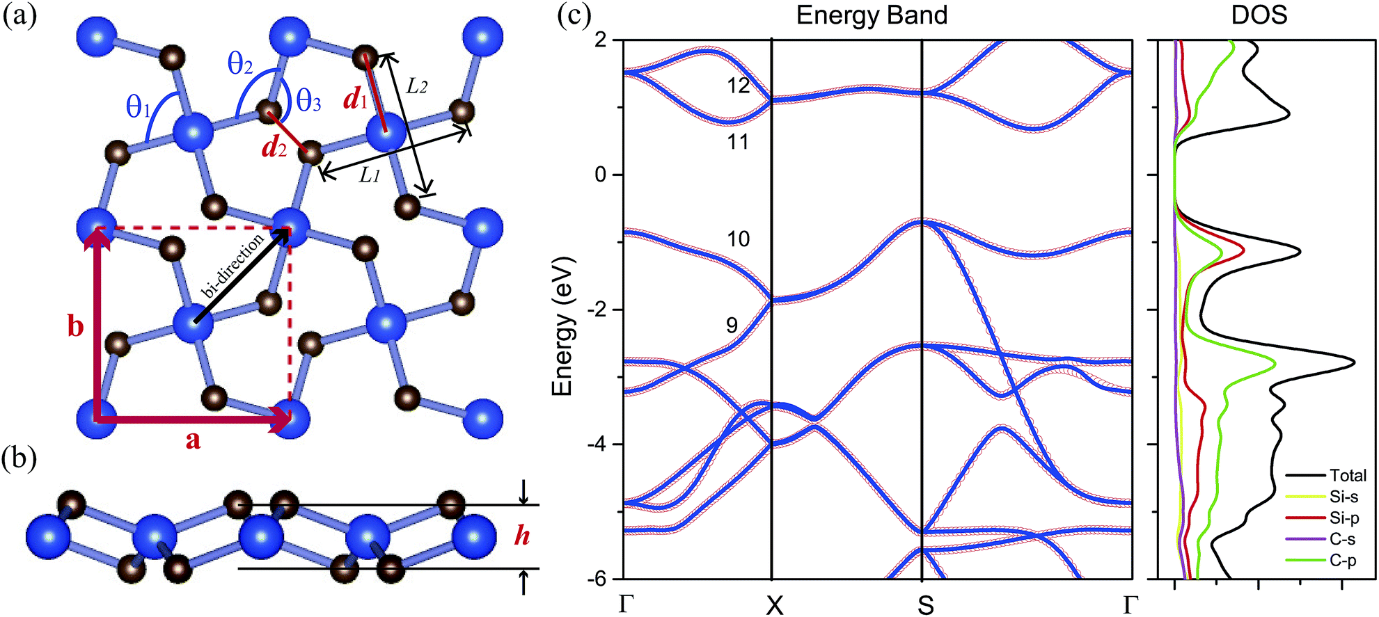 | ||
| Fig. 1 (a) The top view and (b) side view of the atomic structure of the penta-SiC2 monolayer (2 × 2 supercell). d1 and d2 are the bond lengths of Si–C and C–C in this pentagonal structure, respectively. θ1, θ2 and θ3 are the bond angles. h is the buckling distance. (c) PBE calculations of the electronic band structures (red circles) of monolayer penta-SiC2 in comparison to the MLWF-based fitting bands (blue lines), and the density of states (DOS) of penta-SiC2. | ||
| h [Å] | d1 [Å] | d2 [Å] | θ1 [°] | θ2 [°] | θ3 [°] | Eg (PBE/HSE06) [eV] | Y (GPa) |
|---|---|---|---|---|---|---|---|
| 1.33 | 1.91 | 1.36 | 96.94 | 109.57 | 117.40 | 1.39/2.85 | 292 |
The PBE calculations show that SiC2 is a semiconductor with an indirect band gap of 1.39 eV, and the maximum of the valence band (VBM) is located at the S point, and the minimum of the conduction band (CBM) is located between the S and Γ points. The corresponding HSE06 calculation gives a larger band gap of 2.85 eV compared to the PBE result since PBE always underestimates the value of the band gap of semiconductors. Fig. 1(c) shows the PBE calculated electronic band structures and the density of states (DOS) of penta-SiC2. Analysis of the PDOS (Si-3s and 3p and C-2s and 2p orbitals) of penta-SiC2 reveals that the C-2p and Si-3p orbitals mainly dominate the electronic states near the Fermi level. However, the contributions from the C-2p states to the total DOS are larger than those from Si-3p, and in the energy range of −2 to 0 eV for the valence band, the Si-3p states contribute more than the C-2p states, indicating the strong hybridization between the Si-3p states and the C-2p states. The analysis of the chemical bonding of penta-SiC2 based on the DOS is consistent with the calculated bond lengths and bond angles. The four identical bond lengths and bond angles indicate that the fourfold coordinated Si atom connects to the four neighboring C atoms via sp2d-like hybridization,34 although the Si and C atom layers are in different planes, as shown in Fig. 1(b). The chemical bonding analysis of the threefold coordinated C atoms shows that C connects to the two neighboring Si atoms and one C atom via a mixed combination of sp2 and sp3 hybridization, reflected by the bond angles shown in Table 1.
According to the chemical bond analysis of the monolayer penta-SiC2, the band structure near the Fermi level has been calculated based on the projected MLWFs associated with the sp2d-like hybrid orbitals of the fourfold coordinated Si atoms and the sp2 hybrid orbitals of the threefold coordinated C atoms, which fits quite well with the band structure calculated by the standard PBE method based on the plane-wave pseudopotential method, as shown in Fig. 1(b). The aforementioned analysis of the chemical bonds can be reflected by the contour surface plots of the MLWF as well, which is shown in Fig. 2(a) and (d). Only the MLWFs for the 10th and 11th bands near the Fermi level labeled in Fig. 1(c) are shown here.
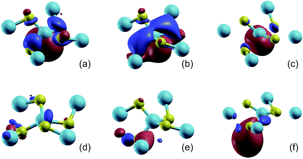 | ||
| Fig. 2 The isosurface plots (iso-value = 2.0) of the MLWFs for penta-SiC2 without strain (a and d), with a uniaxial compressive strain of −10% along the a-direction (b and e), and with a uniaxial tensile strain of 10% along the a-direction (c and f). The MLWFs of (a–c) and (d–f) are associated with the 10th and 11th band, respectively. The band index is labeled in Fig. 1(b). | ||
The isosurface plot of the MLWF associated with the valence band, shown in Fig. 2(b), reveals that the sp2d-like hybridization states of the fourfold coordinated Si atom connecting to the surrounding C atoms determine the valence band of monolayer penta-SiC2, and the pz state of the C atoms also plays an important role. The chemical covalent sp2d-like bond becomes stronger along the L1 direction, shown in Fig. 1(a), when a compressive uniaxial strain of −10% along the a-direction is applied, due to the shorter Si–C bond length, which is shown in Fig. 2(b). However, when applying a tensile uniaxial strain of 10% along the a-direction, the distance of L1 increases further than that of L2, which attenuates the chemical Si–C bonding, especially along the L1 direction. It is shown in Fig. 2(c) that the Si–C bonds along the L2 direction still form sp2d-like hybridization patterns, however, the bonding characteristic of Si–C along the L1 direction becomes very weak and changes obviously. Therefore, the compressive and tensile strains applied to the monolayer penta-SiC2 will distort the lattice and subsequently change the chemical bonding of the Si and C atoms along the directions normal to each other.
The isosurface plot of the MLWF associated with the conduction band, shown in Fig. 2(d), reveals that the sp antibonding states of the threefold coordinated C atoms contribute mainly to the total energy of monolayer penta-SiC2, and the antibonding characteristic does not change for the strained penta-SiC2 when a compressive uniaxial strain of −10% along the a-direction is applied, as shown in Fig. 2(e). However, the tensile strain of 10% along the a-direction stretches the lattice and the chemical bonds of the threefold coordinated C atoms become a  antibonding state, as shown in Fig. 2(f).
Fig. 3 shows the evolution of the valence and conduction band structures as a function of different strains, mainly from −10% to 10% of the fully relaxed structure. Fig. 3(a) and (b) show the dependence of the energy bands of monolayer penta-SiC2 on strain along the a- and bi-directions, respectively. The shift of the band edge as shown in Fig. 3(a) and (b) can be understood in terms of the bonding and antibonding states,35 as described above. The monolayer penta-SiC2 is an indirect semiconductor described by the VBM of VS and the CBM of CS–Γ. Under uniaxial compressive strain, CS–Γ decreases while VS increases, leading to a shrinking indirect band gap of the strained penta-SiC2. The reason why the formation of the indirect band gap of compressively-strained penta-SiC2 remains unchanged is due to the fact that the characteristics of the chemical bonding and antibonding states of the compressive penta-SiC2, which are shown in Fig. 2(b) and (e), respectively, for −10% strain, stay unchanged when a compressive strain is applied, according to the aforementioned bonding analysis.
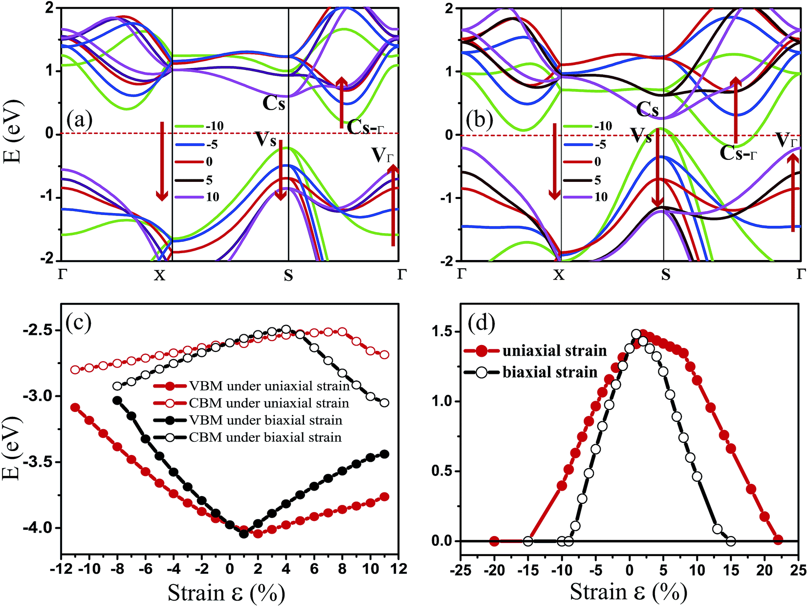 | ||
| Fig. 3 The PBE calculated band structures under (a) uniaxial (a-direction) strain and (b) biaxial (bi-direction) strain for penta-SiC2. (c) shows the change of the CBM/VBM with the applied uniaxial (εx) and biaxial (εxy) strains. (d) shows the evolution of the band gap for penta-SiC2 as a function of εx and εxy. | ||
However, by applying a uniaxial tensile strain, the characteristics of both the chemical bonding and antibonding states of the stretched penta-SiC2 change, which is shown in Fig. 2(c) and (f), respectively, for 10% strain, thus the corresponding band energies change greatly, which transforms the stretched penta-SiC2 into a new type of indirect semiconductor formed by the VBM of VΓ and the CBM of CS.
While for an external strain along the bi-direction (εxy), large changes take place for the energies corresponding to VS, VΓ, CS and CS–Γ, as shown in Fig. 3(b). When εxy = −8%, the semiconductor (indirect)-to-metal transition takes place. The strain tunable electronic structure of monolayer SiC2 will significantly influence the electronic transport properties, which can be used in electronic and optoelectronic applications.
Fig. 3(c) and (d) show the evolution of the calculated band edges (CBM/VBM) and the band gap under various strains. When applying the in-plane uniaxial strain of −15% ≤ εx ≤ 22%, penta-SiC2 remains an indirect semiconductor with a maximum band gap of 1.481 eV at 2%, while the gap values and the positions of the VBM and CBM change. However, when applying the in-plane biaxial strain of −15% ≤ εxy ≤ 15%, penta-SiC2 also retains the indirect semiconducting feature, and it converts into a metal beyond 15% and −9%. The band gap reaches a maximum value of 1.483 eV at the tensile strain of 1%.
Furthermore, to show the contribution of the different orbitals from the different atoms to the electronic states, we have calculated the total (DOS) and partial (PDOS) density of states for penta-SiC2 with tensile and compressive strains: ±10% strains along the a-direction and the bi-direction, respectively, as shown in Fig. 4. By comparison, it’s obvious that the contribution from the different orbitals of the Si and C atoms to the valence band does not change too much when uniaxial or biaxial strain is applied. However, when uniaxial or biaxial compressive strain around εx = −10% is applied, the contribution from the C-2p states becomes dominant in the energy range of 0 to 2 eV for the conduction band. Therefore, when monolayer penta-SiC2 is free of strain or under tensile strain, the conduction band is mainly constructed of the low hybridization states of the Si-3p and C-2p orbitals, and when a large compressive strain is applied, the contribution from the C-2p states overwhelms that from the Si-3p states.
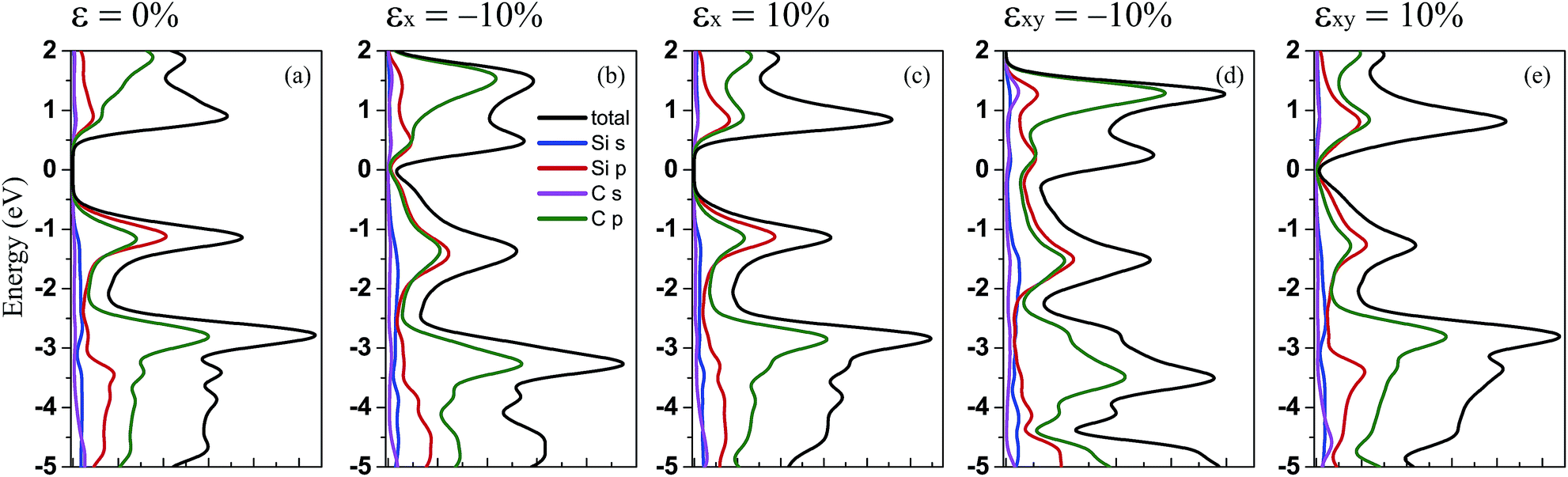 | ||
| Fig. 4 The PBE calculated total and partial density of states for penta-SiC2 under uniaxial and biaxial strain with compressive and tensile strength: (a) no strain, (b) εx = −10%, (c) εx = 10%, (d) εxy = −10%, and (e) εxy = 10%. | ||
3.2 Strain-engineering mechanical properties of penta-SiC2
Since monolayer penta-SiC2 has nearly isotropic physical properties along the a- and b-directions, only the dependence on the strains of εx is considered in the following. Here, εx, εy and εxy refer to the components of the relative strain along the a-, b- and bi(a + b)-directions, respectively. In addition, under the in-plane biaxial strain, the physical properties are nearly the same along the a- and b-directions, so only the physical properties along the b-direction are presented here. Due to three-dimensional (3D) periodic boundary conditions, the 2D elastic constant C2Dij should be rescaled by multiplying the c lattice parameter corresponding to the vacuum space between the 2D layers,36 i.e., C2Dij = c × C3Dij. The calculated in-plane elastic constant C2D11 = C2D22 = 140 N m−1 for penta-SiC2 indicates that penta-SiC2 nearly has isotropic mechanical properties. The positive values of C2D11 and C2D22 mean that penta-SiC2 is mechanically stable, according to the mechanical stability criteria.37 The 3D Young’s modulus Y can be expressed as Y = C2Dij/t, where t is the effective thickness of the penta structure (4.8 Å for penta-SiC2), and the calculated value of Y is 292 GPa for SiC2, similar to that of MoS2 (270 ± 100 GPa (ref. 19)), while it is larger than that of black phosphorene (179 GPa and 55 GPa along the a- and b-directions, respectively38), TiS3 (96 GPa and 153 GPa along the a- and b-directions, respectively24) and HfS2 (137 GPa (ref. 24)). The differences can be attributed to the bond length and the bond density of the different 2D materials.Furthermore, we have calculated the elastic modulus along the a- and b-directions under various mechanical strains, as shown in Fig. 5. By stretching (compressing) the atom–atom bond length, the bond strength decreases (increases) in general due to less (more) overlap of the electron orbitals of the neighboring atoms, partly shown as the isosurface plots of the MLWFs in Fig. 2, which subsequently results in reducing (enlarging) the value of the elastic constants of the strained penta-SiC2. Fig. 5(a) shows the dependence of the elastic constant along the a- and b-directions under uniaxial (εx) strain. Under uniaxial strain, the elastic constant decreases monotonously in the range of −10% ≤ εx ≤ 10% along the b-direction, while along the a-direction, it has a maximum value at a tensile strain of εx = 1% and decreases linearly from εx = 1% to 10%, and under compressive strain, the elastic constant decreases linearly. While for biaxial strain as shown in Fig. 5(b), the value of the elastic modulus of the two directions decreases with a similar tendency to the b-direction under uniaxial strain for penta-SiC2.
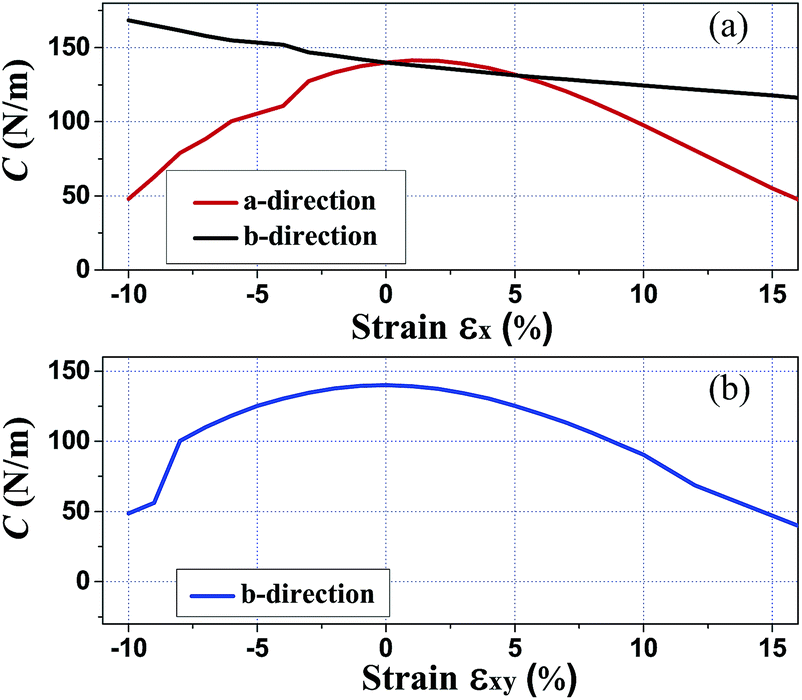 | ||
| Fig. 5 The calculated elastic modulus C2Dij along the a- and b-directions under various mechanical strains for penta-SiC2. | ||
3.3 Strain-engineering transport properties of penta-SiC2
The electron-phonon scatterings play a key role in determining the intrinsic electron transport properties of 2D materials. The deformation potential theory, proposed by Bardeen and Shockley,39 sometimes overestimates the intrinsic mobility at room temperature since it only considers the coupling between electrons and longitudinal acoustic phonons in the long-wavelength limit.40,41 However, it has been reported that the coupling intensity between electrons and acoustic phonons is about 3 times as large as that for the coupling between electrons and optic phonons,42 therefore the carrier mobilities calculated by the deformation potential theory have been reported to be in good consistency with experiments for a series of two-dimensional materials.26,43–45 In the long-wavelength limit, the carrier mobility of a two-dimensional material can be written as26,41,46,47
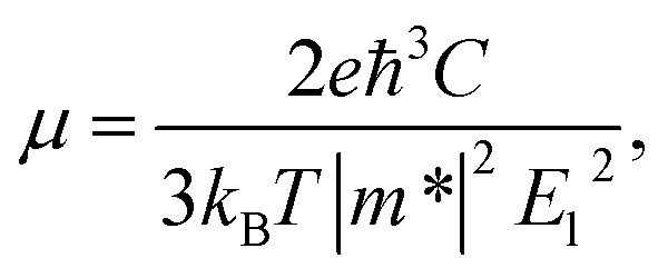 | (1) |
According to eqn (1), the carrier mobility of electrons and holes along certain directions for penta-SiC2 is obtained, as shown in Fig. 6 and Table 3. Although the PBE calculations always underestimate the band gap, the calculated carrier mobilities are in good agreement with the experimental results for many 2D materials.26,41,44,46,48 Firstly, we compared the a-direction uniaxial strain modulated charge carrier mobility of penta-SiC2 along the a- and b-directions, as shown in Fig. 6. Three different physical parameters, namely the carrier effective mass (m*), the DP constant (El) and the elastic modulus (C), are subjected to change at a particular temperature under strain.
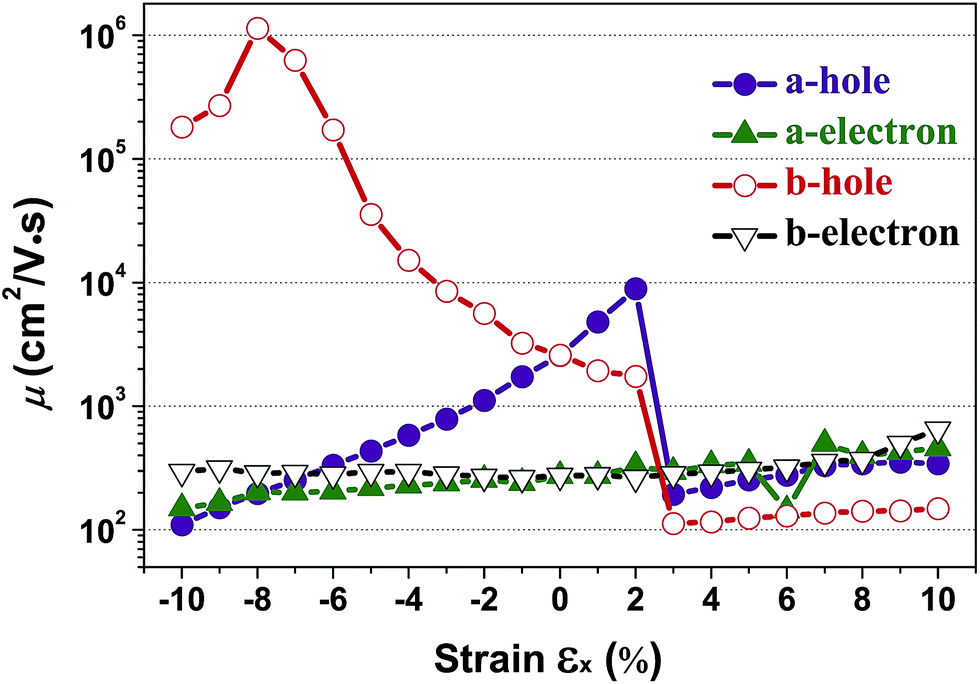 | ||
| Fig. 6 The calculated charge carrier (hole and electron) mobility (μ) along the a- and b-directions as a function of the applied uniaxial strain, respectively. | ||
The band structures of strained penta-SiC2 change when the structure changes, which subsequently alters the effective mass of the carriers determined by the curvatures of the band edges near the Fermi level. Fig. 7 demonstrates the evolution of the calculated effective masses of the electrons  and holes
  along the a- and b-directions under uniaxial strains along the a-direction. The
  at the S point is 0.29m0 and the
  at the S–Γ point is 0.90m0 without strain (m0 is the static electron mass).
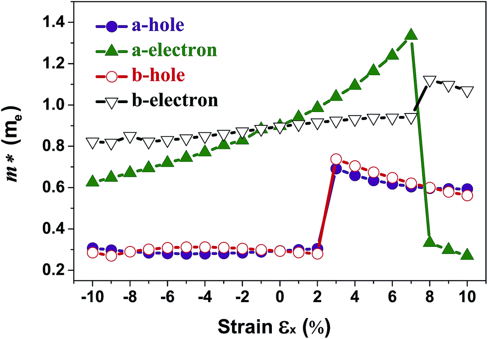 | ||
Fig. 7 The respective dependence of the calculated carrier (hole  and electron and electron  ) effective masses along the a- and b-directions on the applied uniaxial strains. ) effective masses along the a- and b-directions on the applied uniaxial strains. | ||
As shown in Fig. 3(a), the applied strains along the a-direction εx may lead to large shifts of the positions of the VBMs and CBMs in the band structures. The VBM of penta-SiC2 shifts from VS to VΓ with a strain of εx = 3%, which results in a dramatic increase of the  (0.30m0 → 0.69m0 along the a-direction and 0.28m0 → 0.74m0 along the b-direction) when εx increases from 2% to 3%. Meanwhile, the CBM of penta-SiC2 shifts from CS–Γ to CS with an applied strain of εx = 8%. Therefore, a dramatic change of the electron effective mass occurs as well when the uniaxial strain changes from εx = 7% to εx = 8%. The subsequent
  reduces significantly from 1.33m0 to 0.33m0, and the b-direction
  increases from 0.94m0 to 1.12m0, as shown in Fig. 7. Additionally, the anisotropic effective mass under strain will lead to anisotropic carrier mobilities, which finally lead to a direction-dependent electron conductivity.
In order to calculate the DP constant, a small dilation along a special direction needs to be applied. The calculated electron/hole DP constants for unstrained penta-SiC2 are 3.00 eV and 2.98 eV, respectively, which are in good agreement with previous theoretical results.33 Fig. 8 demonstrates the evolution of the electron (El–e) and hole (El–h) DP constants along the a- and b-directions under uniaxial strains along the a-direction. Similar to the case of the effective masses, the shifts of the VBMs with a uniaxial strain of εx = 3% and the CBMs with a strain of εx = 8% cause dramatic changes of the DP constants of the holes and electrons, respectively, as shown in Fig. 8. The nearly flat lines of El–e along the a-direction for εx ranging from −10% to −2%, and El–h along the a-direction for εx ranging from −10% to −8%, as shown in Fig. 8, can be understood by the nearly linear change of the CBM/VBM with εx changing in the corresponding ranges, as shown in Fig. 3(c). The reason is due to the fact that the electron/hole deformation potential constant along the a-direction is approximately the derivative of the CBM/VBM to the strain εx, i.e. El–e/h ≈ (ECBM/VBMl+δl − ECBM/VBMl)/(δl/l).
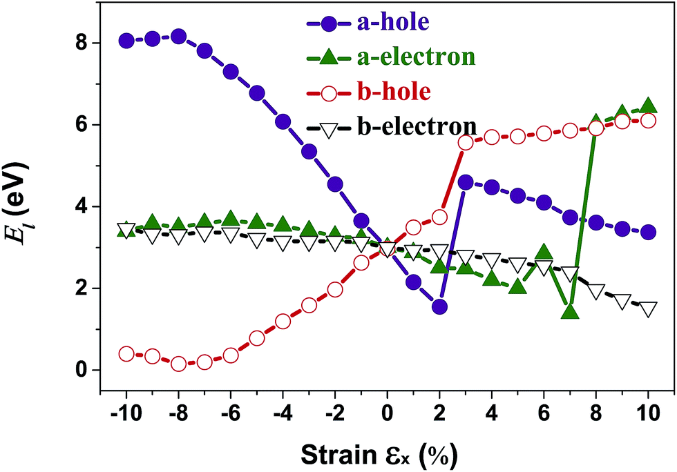 | ||
| Fig. 8 The calculated carrier (hole and electron) deformation potential constant (El) along the a- and b-directions as a function of the applied uniaxial strain. | ||
Interestingly, the obtained b-direction El–h of the holes is low (0.15 eV → 0.40 eV) in the strain range of −10% ≤ εx ≤ 6%, which subsequently results in high hole-carrier mobilities larger than 105 cm2 V−1 s−1 along a particular direction, as shown in Fig. 6.
The dependence of the calculated carrier mobilities on the uniaxial strain is shown in Fig. 6. The obtained hole and electron mobilities without strain are 2.59 × 103 cm2 V−1 s−1 and 2.74 × 102 cm2 V−1 s−1, respectively. For uniaxial strain along the a-direction, a dramatic enhancement of the hole mobility along the b-direction under compressive strains is observed, increasing from 2.59 × 103 cm2 V−1 s−1 to 1.14 × 106 cm2 V−1 s−1 at εx = −8%. In Table 2, the calculated carrier mobilities of strained penta-SiC2 and some widely-investigated two-dimensional semiconductors are listed. By comparison, it is found that the hole carrier mobility of penta-SiC2 strained by εx = −8% is ultrahigh, being an order of magnitude higher than those of graphene (2.58 × 105 cm2 V−1 s−1)49 and silicene (3.39 × 105 cm2 V−1 s−1),49 and three or four orders of magnitude higher than those of monolayer black phosphorene (2.2 × 103 cm2 V−1 s−1)27 and MoS2 (∼200 cm2 V−1 s−1),26,51 which indicates that strain-engineering monolayer penta-SiC2 is quite promising for the application of microelectronic devices. It should be noted that the available range of the compressive or tensile strain is determined by both the method to generate strains and the condition of the mechanical failure of strained materials.52 Common strain-generating methods include lattice mismatch on the substrate, and thermal expansion or mechanical loading, which generally generate strains ranging from −12% to 25%.53 Further stretching or compression should involve an investigation on the stability of strained materials.
| Carrier mobility | Penta-SiC2 | Graphene49 | Silicene49 | BP27,50 | MoS2 (ref. 26 and 51) |
|---|---|---|---|---|---|
| Hole | 1.14 × 10⁶ | 3.51 × 10⁵ | 2.23 × 10⁵ | 286 | 200 |
| Electron | 649 | 3.39 × 10⁵ | 2.58 × 10⁵ | 2.2 × 10³ | 72, ∼200 |
It should be noted that strain-engineering has little influence on the electron mobility along both the a- and b-directions, as shown in Fig. 6. The hole mobility along the a-direction increases nearly linearly from 2.59 × 103 cm2 V−1 s−1 to 1.0 × 104 cm2 V−1 s−1 in the strain range of εx = −10% to 2%, which can be attributed to the monotonic decrease of the effective masses of the holes along the a-direction, according to eqn (1).
Table 3 shows the evolution of the effective mass  , the DP constant (El–b), the elastic modulus (Cb) and the calculated results of the hole and electron mobilities along the b-direction under biaxial strains. For the hole mobility, as listed in Table 3, since all of the three decisive parameters (
 , El–b and Cb) increase by applying tensile and compressive strain, the hole mobilities for the strained structures are thus smaller than that without strain according to eqn (1). The obtained electron mobility increases monotonically from εxy = −10% to εxy = 10%, mainly caused by the decrease of the effective mass
  .
.
 (with
(with  being the static electron mass), the deformation potential constant El–b, the 2D elastic modulus Cb along the Γ–Y direction and the electron/hole carrier mobility μb. The electron and hole carrier mobilities are calculated by using eqn (1) at T = 300 K
| Carrier type | εxy [%] |
|
El–b [eV] | Cb [N m−1] | μb [×102 cm2 V−1 s−1] | Carrier type | εxy [%] |
|
El–b [eV] | Cb [N m−1] | μb [×102 cm2 V−1 s−1] |
|---|---|---|---|---|---|---|---|---|---|---|---|
| Hole | −10 | 0 | 0 | 0 | 0 | Electron | −10 | 0 | 0 | 0 | 0 |
| −8 | 0.29 | 5.45 | 100.37 | 5.78 | −8 | 0.67 | 3.66 | 100.37 | 2.24 | ||
| −6 | 0.30 | 4.78 | 118.29 | 8.43 | −6 | 0.71 | 3.55 | 118.29 | 2.60 | ||
| −4 | 0.30 | 4.12 | 130.41 | 12.31 | −4 | 0.75 | 3.47 | 130.41 | 2.72 | ||
| −2 | 0.30 | 4.03 | 137.66 | 13.68 | −2 | 0.80 | 3.31 | 137.66 | 2.76 | ||
| 0 | 0.29 | 2.99 | 139.89 | 25.88 | 0 | 0.90 | 3.0 | 139.89 | 2.74 | ||
| 2 | 0.66 | 5.29 | 137.31 | 1.58 | 2 | 1.05 | 2.61 | 137.31 | 2.60 | ||
| 4 | 0.55 | 4.80 | 130.34 | 2.65 | 4 | 1.30 | 1.81 | 130.34 | 3.30 | ||
| 6 | 0.48 | 4.34 | 119.47 | 3.91 | 6 | 0.52 | 4.13 | 119.47 | 3.62 | ||
| 8 | 0.43 | 4.00 | 106.01 | 4.99 | 8 | 0.46 | 3.96 | 106.01 | 4.44 | ||
| 10 | 0.40 | 3.62 | 90.39 | 6.03 | 10 | 0.43 | 3.68 | 90.39 | 5.14 |


4 Conclusion
In this paper, we have shown the evolution of the structure, electronic and charge carrier transport properties of penta-SiC2 under uniaxial or biaxial strain, based on first-principles calculations. By calculation, it was found that monolayer penta-SiC2 is a semiconductor with an indirect band gap of 2.85 eV (PBE: 1.39 eV). The transition from semiconductor to metal can take place when applying uniaxial or biaxial strains. The hole mobility along the b-direction can be greatly improved by applying a compressive strain along the a-direction. Meanwhile, strain-engineering has relatively little effect on the electron mobility. The novel and strain-modulated physical properties of monolayer penta-SiC2 may lead to many potential applications in the fields of microelectronic and optoelectronic devices.Conflicts of interest
There are no conflicts to declare.Acknowledgements
This work is supported by the National Natural Science Foundation of China under Grants No. 11374063 and 11404348, and the National Basic Research Program of China (973 Program) under Grant No. 2013CBA01505.References
- K. S. Novoselov, A. K. Geim, S. V. Morozov, D. Jiang, Y. Zhang, S. V. Dubonos, I. V. Grigorieva and A. A. Firsov, Science, 2004, 306, 666–669 CrossRef CAS PubMed.
- K. S. Novoselov, A. K. Geim, S. V. Morozov, D. Jiang, M. I. Katsnelson, I. V. Grigorieva, S. V. Dubonos and A. A. Firsov, Nature, 2005, 438, 197–200 CrossRef CAS PubMed.
- Y. Zhang, Y.-W. Tan, H. L. Stormer and P. Kim, Nature, 2005, 438, 201–204 CrossRef CAS PubMed.
- X. Zhang, H. Zhang, C. Li, K. Wang, X. Sun and Y. Ma, RSC Adv., 2014, 4, 45862–45884 RSC.
- A. A. Alandin, Nat. Mater., 2011, 10, 569–581 CrossRef PubMed.
- A. A. Balandin, S. Ghosh, W. Bao, I. Calizo, D. Teweldebrhan, F. Miao and C. N. Lau, Nano Lett., 2008, 8, 902–907 CrossRef CAS PubMed.
- F. Schedin, A. K. Geim, S. V. Morozov, E. W. Hill, P. Blake, M. I. Katsnelson and K. S. Novoselov, Nat. Mater., 2007, 6, 652–655 CrossRef CAS PubMed.
- S. Balendhran, S. Walia, H. Nili, S. Sriram and M. Bhaskaran, Small, 2015, 11, 640–652 CrossRef CAS PubMed.
- K. Zhou, S. Jiang, C. Bao, L. Song, B. Wang, G. Tang, Y. Hu and Z. Gui, RSC Adv., 2012, 2, 11695–11703 RSC.
- G. Wang, R. Pandey and S. P. Karna, ACS Appl. Mater. Interfaces, 2015, 7, 11490–11496 CAS.
- S. Zhang, J. Zhou, Q. Wang, X. Chen, Y. Kawazoe and P. Jena, Proc. Natl. Acad. Sci. U. S. A., 2015, 112, 2372–2377 CrossRef CAS PubMed.
- W. Xu, G. Zhang and B. Li, J. Chem. Phys., 2015, 143, 154703 CrossRef PubMed.
- H. Liu, G. Qin, Y. Lin and M. Hu, Nano Lett., 2016, 16, 3831–3842 CrossRef CAS PubMed.
- G. R. Berdiyorov and M. E.-A. Madjet, RSC Adv., 2016, 6, 50867–50873 RSC.
- Y. Aierken, O. Leenaerts and F. M. Peeters, Phys. Chem. Chem. Phys., 2016, 18, 18486–18492 RSC.
- A. Lopez-Bezanilla and P. B. Littlewood, J. Phys. Chem. C, 2015, 119, 19469–19474 CAS.
- K. Novoselov and A. C. Neto, Phys. Scr., 2012, 2012, 014006 CrossRef.
- M. Ghorbani-Asl, S. Borini, A. Kuc and T. Heine, Phys. Rev. B: Condens. Matter Mater. Phys., 2013, 87, 235434 CrossRef.
- S. Bertolazzi, J. Brivio and A. Kis, ACS Nano, 2011, 5, 9703–9709 CrossRef CAS PubMed.
- A. Castellanos-Gomez, M. Poot, G. A. Steele, H. S. van der Zant, N. Agraït and G. Rubio-Bollinger, Adv. Mater., 2012, 24, 772–775 CrossRef CAS PubMed.
- J. Feng, X. Qian, C. W. Huang and J. Li, Nat. Photonics, 2012, 6, 866–872 CrossRef CAS.
- H. J. Conley, B. Wang, J. I. Ziegler, J. Richard, F. Haglund, S. T. Pantelides and K. I. Bolotin, Nano Lett., 2013, 13, 3626–3630 CrossRef CAS PubMed.
- S. Yu, H. Zhu, K. Eshun, C. Shi, M. Zeng and Q. Li, Appl. Phys. Lett., 2016, 108, 191901 CrossRef.
- J. Kang, H. Sahin and F. M. Peeters, Phys. Chem. Chem. Phys., 2015, 17, 27742–27749 RSC.
- G. Phan, K. Nakayama, K. Sugawara, T. Sato, T. Urata, Y. Tanabe, K. Tanigaki, F. Nabeshima, Y. Imai and A. Maeda, et al., Phys. Rev. B: Condens. Matter Mater. Phys., 2017, 95, 224507 CrossRef.
- Y. Cai, G. Zhang and Y. Zhang, J. Am. Chem. Soc., 2014, 136, 6269–6275 CrossRef CAS PubMed.
- R. Fei and L. Yang, Nano Lett., 2014, 14, 2884–2889 CrossRef CAS PubMed.
- D. Ã. Yierpan Aierken and F. M. Peeters, Phys. Chem. Chem. Phys., 2016, 18, 14434–14441 RSC.
- G. Kresse and J. Furthmüller, Phys. Rev. B: Condens. Matter Mater. Phys., 1996, 54, 11169–11186 CrossRef CAS.
- J. Heyd, G. E. Scuseria and M. Ernzerhof, J. Chem. Phys., 2003, 118, 8207–8215 CrossRef CAS.
- A. A. Mostofi, J. R. Yates, Y.-S. Lee, I. Souza, D. Vanderbilt and N. Marzari, Comput. Phys. Commun., 2008, 178, 685–699 CrossRef CAS.
- N. Marzari, A. A. Mostofi, J. R. Yates, I. Souza and D. Vanderbilt, Rev. Mod. Phys., 2012, 84, 1419–1475 CrossRef CAS.
- X. Li, Y. Dai, M. Li, W. Wei and B. Huang, J. Mater. Chem. A, 2015, 3, 24055–24063 CAS.
- W. Zhou, M. D. Kapetanakis, M. P. Prange, S. T. Pantelides, S. J. Pennycook and J.-C. Idrobo, Phys. Rev. Lett., 2012, 109, 206803 CrossRef PubMed.
- V. O. Özçelik, O. U. Aktürk, E. Durgun and S. Ciraci, Phys. Rev. B: Condens. Matter Mater. Phys., 2015, 92, 125420 CrossRef.
- M. N. Blonsky, H. L. Zhuang, A. K. Singh and R. G. Hennig, ACS Nano, 2015, 9, 9885–9891 CrossRef CAS PubMed.
- B. Peng, H. Zhang, H. Shao, Z. Ning, Y. Xu, G. Ni, H. Lu, D. W. Zhang and H. Zhu, Mater. Res. Lett., 2017, 5, 399–407 CrossRef.
- Q. Wei and X. Peng, Appl. Phys. Lett., 2014, 104, 251915 CrossRef.
- J. Bardeen and W. Shockley, Phys. Rev., 1950, 80, 72–80 CrossRef CAS.
- Y. Nakamura, T. Zhao, J. Xi, W. Shi, D. Wang and Z. Shuai, arXiv preprint arXiv:1705.01816, 2017.
- J. Chen, J. Xi, D. Wang and Z. Shuai, J. Phys. Chem. Lett., 2013, 4, 1443–1448 CrossRef CAS PubMed.
- L. Tang, M. Long, D. Wang and Z. Shuai, Sci. China, Ser. B: Chem., 2009, 52, 1646–1652 CrossRef CAS.
- R. Wang, B. A. Ruzicka, N. Kumar, M. Z. Bellus, H.-Y. Chiu and H. Zhao, Phys. Rev. B: Condens. Matter Mater. Phys. B, 2012, 86, 045406 CrossRef.
- J. Xi, M. Long, L. Tang, D. Wang and Z. Shuai, Nanoscale, 2012, 4, 4348–4369 RSC.
- S. V. Morozov, K. S. Novoselov, M. I. Katsnelson, F. Schedin, D. C. Elias, J. A. Jaszczak and A. K. Geim, Phys. Rev. Lett., 2008, 100, 16602 CrossRef CAS PubMed.
- M. Long, L. Tang, D. Wang, Y. Li and Z. Shuai, ACS Nano, 2011, 5, 2593–2600 CrossRef CAS PubMed.
- Y. Wang and Y. Ding, Nanoscale Res. Lett., 2015, 10, 254 CrossRef PubMed.
- J. Dai and X. C. Zeng, Angew. Chem., 2015, 127, 7682–7686 CrossRef.
- Z.-G. Shao, X.-S. Ye, L. Yang and C.-L. Wang, J. Appl. Phys., 2013, 114, 093712 CrossRef.
- J. Liu, G.-M. Choi and D. G. Cahill, J. Appl. Phys., 2014, 116, 233107 CrossRef.
- S. Kim, A. Konar, W.-S. Hwang, J. H. Lee, J. Lee, J. Yang, C. Jung, H. Kim, J.-B. Yoo and J.-Y. Choi, et al., Nat. Commun., 2012, 3, 1011 CrossRef PubMed.
- S. Liu, B. Liu, X. Shi, J. Lv, S. Niu, M. Yao, Q. Li, R. Liu, T. Cui and B. Liu, Sci. Rep., 2017, 7, 2404 CrossRef PubMed.
- K. S. Kim, Y. Zhao, H. Jang, S. Y. Lee, J. M. Kim, K. S. Kim, J.-H. Ahn, P. Kim, J.-Y. Choi and B. H. Hong, Nature, 2009, 457, 706 CrossRef CAS PubMed.
| This journal is © The Royal Society of Chemistry 2017 |