
 Open Access Article
 This Open Access Article is licensed under a
 Creative Commons Attribution 3.0 Unported Licence
Athermal repair of nanoscale defects in optical materials using a femtosecond laser†
Qiang
Cao
*a,
Jiajun
Zhang
a,
Jian
Du
b,
Hongming
Zhao
b,
Sheng
Liu
cd and
Qing
Peng
 *cde
*cde
aLaser Micro/NanoFabrication Laboratory, NanoManufacturing Fundamental Research Joint Laboratory of National Science Foundation of China, School of Mechanical Engineering, Beijing Institute of Technology, 100081, PR China. E-mail: caoqiang@bit.edu.cn
bScience and Technology on Special System Simulation Laboratory, Beijing Simulation Center, Beijing, 100854, PR China
cKey Laboratory of Hydraulic Machinery Transient, Ministry of Education, Wuhan University, Wuhan, 430072, China
dThe Institute of Technological Sciences, Wuhan University, Wuhan 430072, China
eNuclear Engineering and Radiological Sciences, University of Michigan, Ann Arbor, MI 48109, USA. E-mail: qpeng.org@gmail.com
First published on 23rd June 2017
Abstract
Ion implantation is widely used to fabricate advanced optical and optoelectronic materials and devices. However, nanoscale defects generated during the ion implantation process severely affect the quality and properties of the material and device. Here, combining computational simulations and experiments, we investigate the mechanism for defect repair in fused silica after Cu ion implantation using femtosecond laser irradiation with an energy fluence much lower than the ablation threshold. Atomic force microscopy demonstrates no unexpected ablation. The optical absorption spectra show that various types of defects with formation energies between 1.9 and 6.2 eV can be repaired successfully via an athermal procedure. The Raman spectra imply that the broken chemical bonds reconnect after femtosecond laser irradiation. Our study reveals that low-energy femtosecond laser irradiation can transfer the appropriate energy needed to repair defects; thus it could be useful in fabricating nonlinear optical devices due to its high spatial selectivity and convenience.
With its high optical nonlinearity and ultrafast response time, fused silica, which is doped with metallic particles by ion implantation, is an attractive material for all-optical communication and optoelectronic devices.1,2 During the ion implantation process, the introduced ions generate trains of defects in lattices.3–16 As illustrated in SRIM (the Stopping and Range of Ions in Matter) model simulations,3–5 the major defects are vacancies and interstitial atoms.6–10 These nanoscale defects severely influence the linear and nonlinear optical properties as well as crystalline construction.3,4 In order to reduce radiation damage, a repair process is followed by or synchronized with ion implantation. Conventionally, thermal annealing is used which heats specimens up to 1300 K. The drawback of this method is that it takes a considerably long time, resulting in a remarkable loss of implanted ions.11 In addition, when the remaining defects producing special properties are desirable, such as absorption humps or an enhancement in electrical resistivity, this method cannot be used because of the lack of spatial selectivity.12,13
Efforts have been made to improve the repair process. Nanosecond laser irradiation after ion implantation has been introduced to decrease the repair time. However, similar to thermal annealing, the method suffers from loss of ions.14 Low-energy nanosecond laser irradiation is also reported to repair lattice defects in ion implantation.15 The non-equilibrium state generated by the interaction between the ions and the material facilitates the energy absorption from the low-energy nanosecond laser, which provides enough energy to shift interstitial atoms to vacancies, avoiding unexpected ablation. However, the setup needs the nanosecond laser system and the ion implantation system to have precise cooperation, which is too complex to be widely used.
For precise and efficient defect repair in the nanoscale, we use a low-energy femtosecond laser to repair lattice defects in Cu ion-implanted fused silica. The process and mechanism of nanodefect repair are investigated. We studied three sets of characterization methods that had shown to prove the effectiveness and selectiveness of this method.
Results and discussion
Characterization using an optical microscope
Pure fused silica is green under an optical microscope as shown in Fig. 1a. After being implanted with Cu ions, the color changed to dark brown (Fig. 1b). When a part of the as-implanted area was irradiated with a femtosecond laser with a fluence of 0.2 J cm−2, the color of the irradiated area changed remarkably (Fig. 1c), similar to that with pure silica. Furthermore, the micro/nanoscale morphology of the area of interest was scanned by atomic force microscopy (AFM). For the as-implanted specimen, there are a great many nanoscale clusters measured about 200 nm wide and 3 nm high. The nanoscale point defects and smaller clusters are along with nanoscale clusters. However, when this as-implanted specimen has been irradiated with the focused low energy femtosecond laser, the number of clusters is substantially reduced. Besides, there are no craters in the irradiated area, implying no unexpected ablation.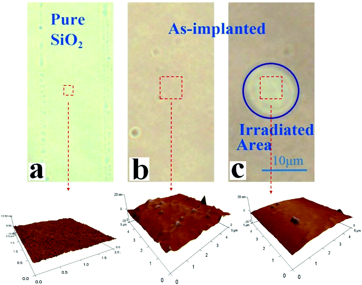 | ||
| Fig. 1 Optical microscopy images and AFM images. The optical microscopy images and related AFM images for (a) pure fused silica, (b) fused silica implanted by the focused Cu ion beam, and (c) as-implanted specimen irradiated by the focused low energy femtosecond laser with a laser fluence of approximately 0.2 J cm−2. | ||
In order to obtain an appropriate laser energy used for irradiation, the laser fluence was varied. When the fluence was above 0.5 J cm−2, an unwanted nanoscale crater in the irradiated area had been observed, which is shown in Fig. S2 in the ESI.† When it was set below 0.1 J cm−2, there was no obvious change of color, completely different from Fig. 1c. The optimized fluence is approximately 0.2 J cm−2, which is much lower than the ablation threshold (2.7 J cm−2) of fused silica.17 Furthermore, to exclude the incubation effects of multiple irradiations which could lead to ablation, the number of laser pulses which stayed at the same point of the sample was reduced to less than 10, and the time interval between two adjacent pulses was set to be longer than 20 milliseconds. So far, for a specimen with an implanted area of 5 × 5 mm2, it takes about half an hour to have most of the defects repaired by this method.
We hypothesize that the Cu atoms and the large number of defects approximately 10 nm below the surface might be responsible for the change in color. In addition, the femtosecond laser irradiation with a laser fluence of 0.2 J cm−2 can affect the distribution of the Cu atoms or the defects.
Optical absorption spectra
To understand the mechanism of the femtosecond laser irradiation method, the optical absorption spectra of both the as-implanted and the irradiated samples have been characterized by using an ultraviolet-visual spectrophotometer, as shown in Fig. 2. For the as-implanted sample, an obvious hump from 200 nm to 650 nm was detected, which gives evidence of defects,18 including the B-band (∼413 nm), non-bridging oxygen holes (∼258 nm), the B2-band (250 nm and 241 nm: oxygen-deficient centers), and E′ centers (214 nm).31,32 Additionally, a peak near 580 nm was also found, which refers to the surface plasmon resonance (SPR) of Cu nanoparticles. After irradiation with the femtosecond laser, the humps decreased by 25% which indicates a reduction in the defects, and the peak disappeared because the Cu nanoparticles could be splintered and re-shaped by the femtosecond laser irradiation.19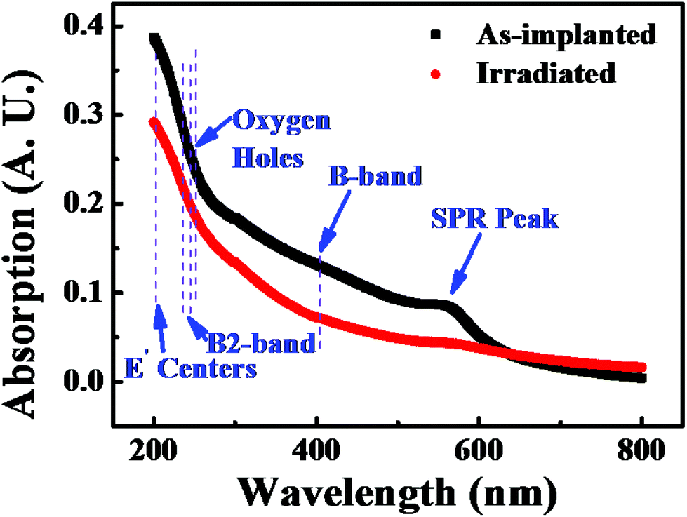 | ||
| Fig. 2 Optical absorption spectra. The optical absorption spectra of the as-implanted specimen (dark square) and the femtosecond laser irradiated area (red circle). The absorption spectra qualitatively show the density of various kinds of defects, such as B-band (413 nm), non-bridging oxygen holes (258 nm), B2-band (250 nm and 241 nm) and E′ centers (214 nm). The reduction of the optical absorption in the irradiated area implies repairing of these defects by the femtosecond laser irradiation. | ||
Raman spectra
To obtain insights into the defect repair mechanism, we studied the Raman spectra of three samples: pure, as-implanted, and irradiated silica (Fig. 3). The spectrum of pure silica has two characteristic peaks which are D1 (492 cm−1) and D2 (605 cm−1). After implantation, a new peak appears at 1579 cm−1, which corresponds to the vibration frequency of O2.20 It means that the Si–O bonds were broken and O-center defects appeared during ion implantation. Additionally, D1 was markedly reduced, and D2 almost disappeared, due to the heavy damage of the lattice construction of fused silica. After femtosecond laser irradiation, however, the peak at 1579 cm−1 was significantly decreased, indicating that the O-center defects were rehabilitated. Additionally, D2 reappeared in the irradiated area, which implies the reconstruction of Si–O bonds. Such a reconstruction instead of destruction of Si–O bonds might be attributed to the fact that the repairing fluence of the femtosecond laser is well below the ablation threshold of silica.34 We might conclude that the low fluence that is smaller than the ablation threshold fluence of the femtosecond laser could be the key for defect repair.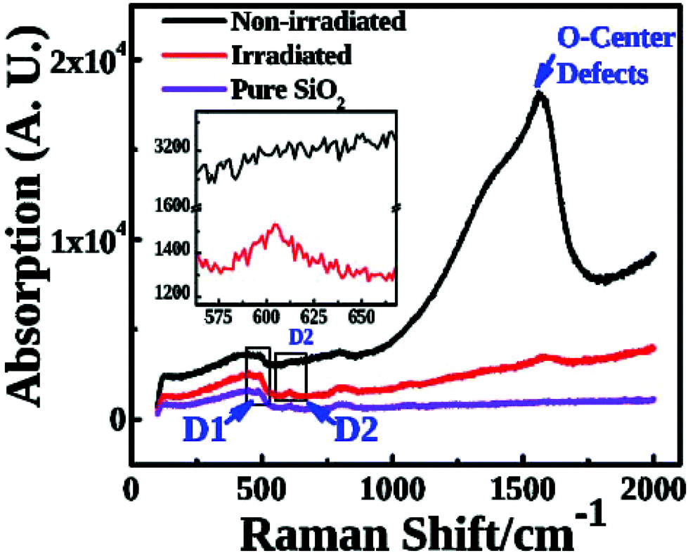 | ||
| Fig. 3 Raman spectrum. The Raman spectrum of the pure fused silica (violet line), as-implanted specimen without irradiation (dark line), and as-implanted specimen with femtosecond laser irradiation (red line). For pure fused silica, there are two characteristic peaks of the Si–O bonds, D1 (492 cm−1) and D2 (605 cm−1). For the as-implanted specimen, D2 almost disappears, shown in the inset, and a new peak appears at 1579 cm−1, which means that the Si–O bonds were broken and the O-center defects appeared after ion implantation. For the irradiated specimen, D2 grows up again, shown in the inset, and the peak of the O-center defects drops dramatically. The inset is the zoom-in view of plots around D2 for a better view. | ||
Copper is well known to be extremely mobile within materials, diffusing along interfaces and defects in materials under a host of different environmental factors. As such, the effective control of copper suspensions is critical for defect repair. We found that the copper could exist in two types in our cases: Cu nanoparticles and CuO compounds. Once the Cu ions were implemented with a fluence of 3 × 1017 cm−2, there were saturated Cu ions which aggregate and form nanoparticles. This could be verified by the SPR peak shown in Fig. 2. The Raman spectra (Fig. 3) also show the existence of Cu nanoparticles. When irradiated by using the femtoscecond laser, Cu atoms react with SiO2 to form CuO. In the meantime, some Cu oxide compounds could form Cu atoms which then aggregate into nanoparticles. The concentrations of Cu nanoparticles and compounds depend on the energy density and time duration of the femtosecond laser radiation. It is worth mentioning that we did not observe the loss of Cu in our study as there is no ablation during our low energy fluence femtosecond laser radiation.
To gain more insight into the defect repair, we carried out a simulation of the elemental copper distribution via Stopping and Range of Ions in Matter (SRIM) modeling. The details are in the following simulation subsection. It can be seen that a high concentration of Cu ions is implanted in the target's surface with a depth of approximately 70 to 300 nm (Fig. 4). At the same time, a train of defects, including vacancies and interstitial atoms, were formed in the material, which can be seen in Fig. 5. The higher the voltage is, the deeper the ions reach and the more defects exist.
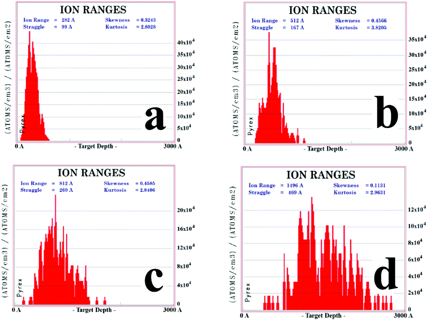 | ||
| Fig. 4 Distribution of the copper atoms. The simulation of the SRIM model shows the distribution of the Cu density to the depth. 200 copper ions are injected into fused silica. The acceleration voltages are (a) 30 kV, (b) 60 kV, (c) 100 kV and (d) 190 kV, respectively. | ||
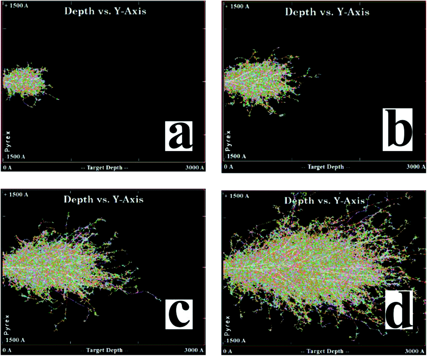 | ||
| Fig. 5 The SRIM model simulation shows the trace of the copper and the defects induced by copper ions. 200 copper ions are injected into fused silica from left to right. The acceleration voltages are (a) 30 kV, (b) 60 kV, (c) 100 kV and (d) 190 kV, respectively. The red point indicates a point defect. | ||
Simulations using the SRIM model
To figure out the distribution of the defects induced by the collision between copper ions and fused silica, a SRIM model was built to simulate the process of ion implantation with the acceleration voltages of 30, 60, 100 and 190 kV, in which 60 kV was the most commonly used. The results are shown in Fig. 4. For an acceleration voltage of 30 and 60 kV, Cu ions are implanted in the target's surface with a depth of approximately 300 nm, and the distribution is a Gaussian shape. For 100 and 190 kV, the distributions become irregular and much deeper. Generally, the densities at the surface and the deep end are much smaller, and the density at the middle is obviously larger. No matter how big the voltage is, the ions are localized at the very shallow surface. It can be seen that a high concentration of Cu ions is implanted in the target's surface with a depth approximately 70 to 300 nm. This localization of Cu ions is a good property for micro/nano-fabrication.Our simulation also shows that at the same time of ion implantation, a train of nanoscale defects, including vacancies and interstitial atoms, are formed in the material, which can be seen in Fig. 5 for the ion implantation with the acceleration voltages of 30, 60, 100 and 190 kV, respectively. Point defects are introduced during collisions between the implanted ions and atoms in the matrix. Avalanche collisions are induced by the recoil atoms. When the kinetic energy is large enough to kick the atom away from the lattice, there will be a vacancy marked in the figure. The higher the voltage is, the deeper the ions reach and the more defects exist. As the voltage grows larger, the defects expand dramatically in a direction parallel to the surface. The depth of the defects is 1.5 times that of the depth of ions due to the recoil atoms. In addition, the higher the voltage is, the deeper the ions reach and the more defects exist. Despite these variations, the processes stay at almost the same level and the evolution after femtosecond laser irradiation is considered to be similar.
Repair process
The evolution of the molecular structures during the repair process is derived from the three sets of aforementioned characterization. Firstly, for the as-implanted specimen, SiO2 molecules were splintered by the introduced Cu particles and Si–O bonds were broken. O-Center defects appeared, as shown schematically in Fig. 6a. Then it was irradiated with a low-energy femtosecond laser. In this stage, energy in electromagnetic radiation is transferred to the electrons promoting them from their ground state into some excited state. Due to their much smaller mass, electrons move much faster than ions. Electron–electron collisions are prominent in energy transfer, resulting in the electronic energies adopting a Fermi–Dirac distribution defining an electronic temperature. The maximum electronic temperature will be achieved in approximately 0.1 picoseconds. The energy is then transferred to the ions, via electron–phonon coupling, leading to an increase in the ionic temperature or lattice temperature. The lattice will melt if the ionic temperature is higher than the melting temperature. This process is called thermal melting and it takes on the order of a few picoseconds. For femtosecond laser irradiation, a large fraction (10% or more) of the valence electrons will be excited to conduction electrons33 and free electrons (Fig. 6c) which strongly modify the interatomic forces, resulting in coherent atomic motions and the irradiated sample will melt on time scales shorter than the thermal melting. The displaced atoms obtain the laser energy in the energy transition (Fig. 6c). Some of them possess enough kinetic energy to move back to some vacant positions. As a result, the chemical bonds are recovered and the defects are repaired (Fig. 6d).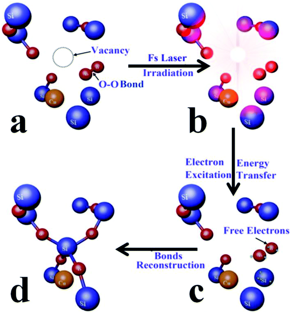 | ||
| Fig. 6 Repair process. The schematic diagram of the nanoscale defects repair process in four stages, as (a) defects in fused silica implanted by the focused Cu ion beam, (b) precisely controlled femtosecond laser irradiation with a laser fluence approximately 0.2 J cm−2, (c) energy transition from the electromagnetic field to electrons, and (d) bond reconstruction. | ||
Additionally, the copper suspensions are roughly controlled by the low-energy femtosecond laser irradiation. The copper atoms irradiated by the femtosecond laser begin to accumulate. When the density of the localized copper atoms reaches a certain degree, the Cu nanoparticles were separated out in fused silica, which would play an important role in enhancing the useful nonlinear properties of the material. Furthermore, no copper particles are found on the surface of fused silica from the AFM images, which means that the ejection of large amounts of copper atoms did not happen.
Compared with traditional thermal annealing methods, femtosecond laser irradiation achieves high spatial selectivity because the focused laser can be applied selectively to small areas that require reparation, as shown in Fig. 1c. When remaining defects producing special properties are desirable, such as producing some absorption humps or an enhancement in electrical resistivity, the selectivity of repair could be very useful. In comparison with a nanosecond laser, femtosecond laser irradiation has much less loss of metallic particles. Both experiments21–24 and calculations25,26 have shown that nanosecond laser irradiation can lead to rapid melting of the material and hence annihilate the defects. The advantage of the femtosecond laser over nanosecond laser irradiation is that there is no unexpected ablation, there are no remaining metallic particles in the specimen, and the rapid repair of defects is achieved.
The reason for the effective defect repair in our study could be the optimization of two competing factors, laser fluence and pulse duration. On one hand, the laser is strong enough to cause the excitation of a large fraction of valence electrons. On the other hand, the femtosecond laser has a much shorter pulse duration, which is even shorter than the electron–lattice relaxation time to avoid ablation. Therefore, the laser energy absorption is completed during the non-thermal process in significant electron–lattice non-equilibrium states.27–30
It is worth noting that this approach of athermal reparation of nanoscale defects via a femtosecond laser is only applicable to optical materials so that the laser can penetrate into the bulk and effectively have the nanoscale defect repaired. In addition, though high spatial selectivity and low efficiency seem to be two sides of the same coin in this study, our approach could be combined with other thermal and ionization processes35 to further improve the efficiency of defect reparation.
Conclusion
In conclusion, a low energy femtosecond laser has been used to repair the nanoscale defects in fused silica after Cu ion implantation. The optimized laser fluence is approximately 0.2 J cm−2, which is much lower than the ablation threshold. We investigated the mechanism of defect repair in fused silica after Cu ion implantation using femtosecond laser irradiation with an energy fluence much lower than the ablation threshold. The optical absorption spectra show that the defects can be repaired. The Raman spectra imply that the broken chemical bonds reconnect after the femtosecond laser irradiation. All three sets of characterization showed that interstitial atoms caused by the introduced ions could gain suitable energy to fit vacancies, and then the broken chemical bond recovered. The mechanism of the defect repair in our femtosecond laser irradiation treatment is athermal due to the strongly modified inter-atomic forces caused by the excitation of electrons.Experimental setup and methods
The fused silica specimens of 10 mm × 10 mm and 1 mm thickness had both surfaces polished, and then were implanted by using a MEVVA ion implanter. The ion beam was Cu with 60 kV acceleration voltage. The dose rate was 2 μA cm−2 and the total dose used for the experiment was 3 × 10¹⁷ ions per cm2.The laser used in the experiment was a commercial chirped-pulse regenerative oscillator-amplifier femtosecond laser system (MaiTai, Spectra-Physics). The laser pulse was linearly polarized, with a central wavelength of 800 nm, a pulse width of 50 fs (FWHM), and a repetition rate of 1 kHz. The fundamental energy is attenuated to the desired level by using a neutral density filter. The pulse was focused on the specimens’ surface at normal incidence using a 5× microscope objective lens (NA = 0.13, Olympus), which generated a spot with a diameter of approximately 9 μm. The fused silica substrate was mounted onto a translation stage. To create a suitable irradiation area, the fused silica substrate was translated relative to the laser beam, exposing any given spot on the silicon surface to an average of 100 pulses. The optical properties of the as-implanted silica before and after laser irradiation, as well as pure silica, were characterized by using an optical microscope (BX51, Olympus). The absorption spectra were obtained by using an ultraviolet-visual spectrophotometer (Lambda 35, PE) and the information of lattice defects was characterized by using a Raman spectrometer (inVia-Reflex, Renishaw). The topography of the surface was observed by using an atomic force microscope (Dimension Edge, Bruker).
SRIM simulations details
SRIM, a package of computer programs which calculate the interactions of ions with matter, is based on a Monte Carlo simulation method, the binary collision approximation with a random selection of the impact parameter of the next colliding ion. The SRIM model assumes that when an atom/ion collides with a target atom in the lattice and the energy Etrans transferred from the incident atom/ion is larger than the displacement energy Edisp, which is the energy used to kick the target atom away from the lattice with a certain distance so that it cannot restore immediately, the target atom will be kicked away from the lattice. Because of the minimum energy loss Elatt used for the atom displacement from the lattice, the recoil energy of the displaced atom is derived from Erecoil = Etrans − Elatt. If Erecoil is larger than Edisp, it will collide with other target atoms and more defects of vacancies and interstitial atoms could exist.The defect types and their dynamic distributions are important in the process of defect repairs. To shed more light on this, we studied the distribution of the oxygen and silicon atoms through the SRIM simulations for the ion implantation with acceleration voltages of 30, 60, 100 and 190 kV, respectively. The results are shown in Fig. 7. We observed that the number of recoil oxygen atoms is much larger than silicon for the simple reason that oxygen is easier to be knocked away from the lattice by copper ions than silicon due to the lighter mass. The recoil oxygen atoms contribute large numbers of defects. The distribution of recoil atoms is similar to that of the copper ions in Fig. 4, which means that the number of recoil atoms is roughly decided by the number of copper atoms.
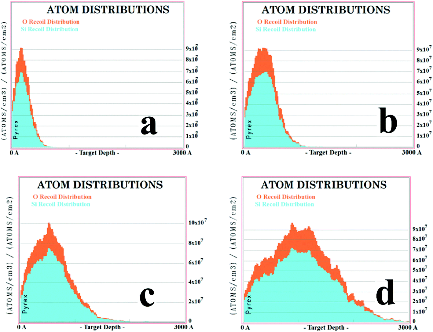 | ||
| Fig. 7 Distribution of the oxygen and silicon atoms. The SRIM model simulation shows the distribution of the recoiled oxygen (yellow) and silicon (blue) atoms density with respect to the depth. The acceleration voltages are (a) 30 kV, (b) 60 kV, (c) 100 kV and (d) 190 kV, respectively. | ||
Author contributions
Q. C. designed the project design. J. Z. and Q. C. performed the majority of experiments. Q. C., J. Z., and Q. P. wrote the paper. J. D. and H. Z. did the simulations of the process of ion implantation. Q. P., Q. C., and S. L. performed data analysis and revised the paper. All authors discussed the results and commented on the manuscript.Competing financial interests
The authors declare no competing financial interests.Acknowledgements
This work was supported by the National Science Foundation of China (NSFC) (grants 91323301 and 51375051) and the Open Research Fund of Key Laboratory of High Performance Complex Manufacturing, Central South University.References
- K. Fukumi, A. Chayahara, K. Kadono, T. Sakaguchi, Y. Horino and M. Miya,
et al., Gold nanoparticles ion implanted in glass with enhanced nonlinear optical properties, J. Appl. Phys., 1994, 75, 3075–3080 CrossRef CAS
.
- B. Can-Uc, R. Rangel-Rojo, H. Márquez, L. Rodríguez-Fernández and A. Oliver, Nanoparticle containing channel waveguides produced by a multi-energy masked ion-implantation process, Opt. Express, 2015, 23, 3176 CrossRef CAS PubMed
- W. Primak and R. Kampwirth, The radiation compaction of vitreous silica, J. Appl. Phys., 1968, 39, 5651–5658 CrossRef CAS
- S. H. Pan, D. Recht, S. Charnvanichborikarn, J. S. Williams and M. J. Aziz, Enhanced visible and near-infrared optical absorption in silicon supersaturated with chalcogens, Appl. Phys. Lett., 2011, 98, 14–17 Search PubMed
- J. F. Ziegler, M. D. Ziegler and J. P. Biersack, Nuclear Instruments and Methods in Physics Research B SRIM – The stopping and range of ions in matter (2010), Nucl. Instrum. Methods Phys. Res., Sect. B, 2010, 268, 1818–1823 CrossRef CAS
- Q. Peng, W. Ji and S. De, First-principles study of the effects of mechanical strains on the radiation hardness of hexagonal boron nitride monolayers, Nanoscale, 2013, 5, 695–703 RSC
- Q. Peng, W. Ji, H. Huang and S. De, Stability of self-interstitial atoms in hcp-Zr, J. Nucl. Mater., 2012, 429, 233–236 CrossRef CAS
- Q. Peng, W. Ji, H. Huang and S. De, Axial ratio dependence of the stability of self-interstitials in HCP structures, J. Nucl. Mater., 2013, 437, 293–296 CrossRef CAS
- Q. Peng, W. Ji, J. Lian, X. Chen, H. Huang and F. Gao,
et al., Pressure effect on stabilities of self-interstitials in HCP-zirconium, Sci. Rep., 2014, 4, 5735–5741 CrossRef CAS PubMed
-
Q. Peng, X. Zhang and G. Lu, Structure, mechanical and thermodynamic stability of vacancy clusters in Cu, 2010, vol. 18, pp. 1–17 Search PubMed
- R. A. Wood, P. D. Townsend, N. D. Skelland, D. E. Hole, J. Barton and C. N. Afonso, Annealing of ion implanted silver colloids in glass, J. Appl. Phys., 1993, 74, 5754–5756 CrossRef CAS
- Y. Takeda, V. Gritsyna, N. Umeda, C. Lee and N. Kishimoto, Linear and nonlinear optical properties of Cu nanoparticles fabricated by high-current Cu− implantation in silica glass, Nucl. Instrum. Methods Phys. Res., Sect. B, 1999, 148, 1029–1033 CrossRef CAS
- S. Kohiki, M. Nishitani, T. Wada and T. Hirao, Enhanced conductivity of zinc oxide thin films by ion implantation of hydrogen atoms, Appl. Phys. Lett., 1994, 64, 2876–2878 CrossRef CAS
- G. Battaglin, E. Borsella, E. Cattaruzza, F. Gonella, R. F. Haglund and G. Mattei,
et al., Highly nonlinear optical composites obtained in silica and soda-lime glasses by Ti ion implantation and laser annealing, Nucl. Instrum. Methods Phys. Res., Sect. B, 1998, 141, 274–278 CrossRef CAS
-
N. Kishimoto, N. Okubo, N. Umeda and Y. Takeda, Laser-induced bleaching of insulators under MeV heavy-ion implantation, ed. Nanosci Using Laser-Solid Interact, 2002, vol. 4636, pp. 88–96 Search PubMed
- L. Porte, M. Phaner, C. H. de Villeneuve, N. Moncoffre and J. Tousset, Scanning tunneling microscopy study of single-ion impacts on graphite surface, Nucl. Instrum. Methods Phys. Res., Sect. B, 1989, 44, 116–119 CrossRef
- B. Chimier, O. Utéza, N. Sanner, M. Sentis, T. Itina and P. Lassonde,
et al., Damage and ablation thresholds of fused-silica in femtosecond regime, Phys. Rev. B: Condens. Matter, 2011, 84, 94104 CrossRef
- Y. Takeda, J. P. Zhao, C. G. Lee, V. T. Gritsyna and N. Kishimoto, Nonlinear optical properties of Cu nanoparticles embedded in insulators by high-current Cu− implantation, Nucl. Instrum. Methods Phys. Res., Sect. B, 2000, 166–167, 877–881 CrossRef CAS
- A. A. Unal, A. Stalmashonak, H. Graener and G. Seifert, Time-resolved investigation of laser-induced shape transformation of silver nanoparticles, Phys. Rev. B: Condens. Matter Mater. Phys., 2009, 80, 1–7 CrossRef
- K. Tomiyasu, Traditional Topics, New Methods in Electrical Measurements, Phys. Today, 1968, 21, 107 CrossRef
- D. H. Auston, C. M. Surko, T. N. C. Venkatesan, R. E. Slusher and J. A. Golovchenko, Time-resolved reflectivity of ion-implanted silicon during laser annealing, Appl. Phys. Lett., 1978, 33, 437 CrossRef CAS
- C. W. White, W. H. Christie, B. R. Appleton, S. R. Wilson, P. P. Pronko and C. W. Magee, Redistribution of dopants in ion-implanted silicon by pulsed-laser annealing, Appl. Phys. Lett., 1978, 33, 662 CrossRef CAS
- C. W. White, P. P. Pronko, S. R. Wilson, B. R. Appleton, J. Narayan and R. T. Young, Effects of pulsed ruby-laser annealing on As and Sb implanted silicon, J. Appl. Phys., 1979, 50, 3261 CrossRef CAS
- J. Narayan, Depth of melting produced by pulsed-laser irradiation, Appl. Phys. Lett., 1979, 34, 312 CrossRef CAS
- J. C. Wang, R. F. Wood and P. P. Pronko, Theoretical analysis of thermal and mass transport in ion-implanted laser-annealed silicon, Appl. Phys. Lett., 1978, 33, 455 CrossRef CAS
- P. Baeri, S. U. Campisano, G. Foti and E. Rimini, A melting model for pulsing-laser annealing of implanted semiconductors, J. Appl. Phys., 1979, 50, 788 CrossRef CAS
-
C. Wang, L. Jiang, F. Wang, X. Li, Y. P. Yuan and H. L. Tsai, First-principles calculations of the electron dynamics during femtosecond laser pulse train material interactions, 2011, DOI:10.1016/j.physleta.2011.07.009
- L. Jiang, P. Liu, X. Yan, N. Leng, C. Xu and H. Xiao,
et al., High-throughput rear-surface drilling of microchannels in glass based on electron dynamics control using femtosecond pulse trains, Opt. Lett., 2012, 37, 2781 CrossRef CAS PubMed
- L. Jiang, X. Shi, X. Li, Y. Yuan, C. Wang and Y. Lu, Subwavelength ripples adjustment based on electron dynamics control by using shaped ultrafast laser pulse trains, Opt. Express, 2012, 20, 21505 CrossRef PubMed
- N. Zhang, X. Li, L. Jiang, X. Shi, C. Li and Y. Lu, Femtosecond double-pulse fabrication of hierarchical nanostructures based on electron dynamics control for high surface-enhanced Raman scattering, Opt. Lett., 2013, 38, 3558 CrossRef CAS PubMed
- Z. Zhu, P. Jung and E. Langenscheidt, Optical absorpion in proton-irradiated vitreous silica and its dependence on irradiation conditions and annealing, J. Non-Cryst. Solids, 1997, 217, 173–181 CrossRef CAS
- M. Guzzi, M. Martini, A. Paleari, F. Pio, A. Vedda and C. B. Azzoni,
et al., Neutron irradiation effects in amorphous SiO2: optical absorption and electron paramagnetic resonance, J. Phys.: Condens Matter, 1993, 5, 8105–8116 CrossRef CAS
- A. Rousse, C. Rischel, S. Fourmaux, I. Uschmann, S. Sebban and G. Grillon,
et al., Non-thermal melting in semiconductors measured at femtosecond resolution, Nature, 2001, 410, 65–68 CrossRef CAS PubMed
- C. S. R. Nathala, A. Ajami, W. Husinsky, B. Farooq, S. I. Kudryashov and A. Daskalova,
et al., Ultrashort laser pulse ablation of copper, silicon and gelatin: effect of the pulse duration on the ablation thresholds and the incubation coefficients, Appl. Phys. A, 2016, 122, 107 CrossRef
- Y. Zhang, R. Sachan, O. H. Pakarinen, M. F. Chisholm, P. Liu and H. Xue,
et al., Ionization-induced annealing of pre-existing defects in silicon carbide, Nat. Commun., 2015, 6, 8049 CrossRef CAS PubMed
Footnote |
| † Electronic supplementary information (ESI) available: AFM images of the femtosecond laser irradiated areas. See DOI: 10.1039/c7nr01599b |
| This journal is © The Royal Society of Chemistry 2017 |