
 Open Access Article
 This Open Access Article is licensed under a
 Creative Commons Attribution 3.0 Unported Licence
Progress in piezo-phototronic effect enhanced photodetectors
Xun
Han
a,
Mengxiao
Chen
a,
Caofeng
Pan
*a and
Zhong Lin
Wang
ab
aBeijing Institute of Nanoenergy and Nanosystems, Chinese Academy of Sciences, National Center for Nanoscience and Technology (NCNST), Beijing, 100083, P. R. China. E-mail: cfpan@binn.cas.cn
bSchool of Materials Science and Engineering, Georgia Institute of Technology, Atlanta, GA 30332-0245, USA
First published on 8th November 2016
Abstract
Wurtzite structured materials such as InN, CaN, ZnO, and CdSe simultaneously possess piezoelectric, semiconducting, and photoexcitation properties. The piezo-phototronic effect utilizes the piezo-polarization charges induced in the vicinity of the interface/junction to regulate the energy band diagrams and modulate charge carriers in the optoelectronic processes, such as transport, generation, recombination, and separation. This article reviews recent progress in piezo-phototronic effect enhanced photodetectors, starting from the fundamental physics, following the development from a single nanowire device to a large-scale photodetector array for illumination imaging. The piezo-phototronic effect provides a promising approach to improve the performance of the wurtzite structured material-based photodetectors. It may have potential applications in optical communication, optoelectronic devices, and multifunctional computing systems.
 Xun Han | Xun Han received his undergraduate degree from Shandong University in 2012. Currently he is pursuing his PhD under the supervision of Prof. Caofeng Pan at Beijing Institute of Nanoenergy and Nanosystems, Chinese Academy of Sciences. His research is mainly focused on piezotronics and piezo-phototronics and their applications in human electronics interfacing. |
 Mengxiao Chen | Mengxiao Chen received her BS in physics from Northeastern University in 2012 and is currently a PhD student with Prof. Z. L. Wang at Beijing Institute of Nanoenergy and Nanosystems, CAS. She is interested in novel self-powered systems and multifunctional photoelectric devices, and is now focused on electronic applications of piezo-phototronics. |
 Caofeng Pan | Caofeng Pan received his BS degree (2005) and his PhD (2010) in Materials Science and Engineering from Tsinghua University, China. He then joined the group of Professor Zhong Lin Wang at the Georgia Institute of Technology as a postdoctoral fellow. He is currently a professor and a group leader at Beijing Institute of Nanoenergy and Nanosystems, Chinese Academy of Sciences, since 2013. His main research interests focus on the fields of piezotronics/piezo-phototronics for fabricating new electronic and optoelectronic devices and self-powered nanosystems. Details can be found at http://piezotronics.binncas.cn/. |
 Zhong Lin Wang | Zhong Lin (ZL) Wang is the Hightower Chair in Materials Science and Engineering, Regents' Professor, at Georgia Institute of Technology. He is also the chief scientist and director of the Beijing Institute of Nanoenergy and Nanosystems, Chinese Academy of Sciences. Prof. Wang has made original and innovative contributions to the synthesis, characterization, and fundamental physical properties of oxide nanobelts and nanowires. He is the lead figure in ZnO nanostructure research. His discovery and breakthroughs in developing nanogenerators established the principle and technological road map for harvesting mechanical energy from the environment and biological systems for powering personal electronics. He coined and pioneered the field of piezotronics and piezo-phototronics. |
1. Introduction
Sensing elements are essential components in electronic industries.1–5 They play an important role in integrated systems e.g. thermal sensing,6 trouble sensing, and strain sensing elements.7–12 Based on them, it becomes feasible to make instruments multifunctional.13 Among all the newly developed sensors, optoelectronic sensors have attracted attention from researchers in many fields because of their wide applications in modern electronics.14–18 Realization of optoelectronic sensing can further open up areas in wearable devices, health care, and environmental monitoring.19,20 This is highly dependant on the performance of photodetectors, which work as the photosensing components.21–24 To fulfil the growing demands of high-performance photosensing devices, tremendous efforts have been devoted to this and the third generation semiconductor is believed to be a potential material to optimize the performance.25–27 Piezoelectric semiconducting materials (the third generation semiconductor) with a wurtzite structure, such as InN, GaN, ZnO, and CdSe, have outstanding optical and electrical properties, so they can be candidates for high-performance photodetectors.28–31Recently, investigations on the coupling among piezoelectric polarization, semiconductor properties, and photon excitation under mechanical stimuli have led to an interdisciplinary field of piezo-phototronics.32–34 This effect has been introduced in GaN, ZnO, and other wurtzite structured piezoelectric semiconductors.35–41 In this kind of material, the induced piezoelectric polarization charges upon straining can effectively tune the energy band diagram at the local interface and modulate charge carriers in the optoelectronic processes, such as transport, generation, recombination, and separation.42 Novel fundamental phenomena and unprecedented applications could be expected.43–52 Here, we review the fundamental physics and recent important developments of the piezo-phototronic effect enhanced photodetectors from single nanowire devices to light distribution imaging applications.
2. Fundamentals of the piezo-phototronic effect
2.1 Piezopotential
Wurtzite structured materials, such as InN, GaN, ZnO, and CdSe, simultaneously possess piezoelectric and semiconductor properties. A wurtzite semiconductor (e.g. ZnO) shows an anisotropic property in the c-axis direction and perpendicular to the c-axis. The Zn2+ cations and O2− anions are tetrahedrally coordinated and the centers of the positive ions and negative ions overlap with each other. When there is pressure applying on an apex of a tetrahedron, the center of the anions and the center of the cations are displaced relatively, leading to a dipole moment (Fig. 1a). The accumulation of the dipole moments from all units in the crystal creates a piezoelectric field along the straining direction in the crystal.53,54 This is the piezoelectric potential (piezopotential) (Fig. 1b),55,56 which exists as long as the strain is statically applied. The coupling piezoelectric, semiconducting, and photoexcitation properties have led to the new fields of piezotronics and piezo-phototronics (Fig. 1c).57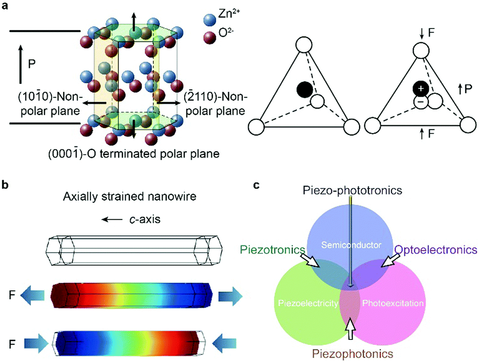 | ||
| Fig. 1 Piezopotential introduced by strain in the ZnO wurtzite crystal. (a) The wurtzite structured ZnO atomic model. Reproduced with permission.60 Copyright 2012, Wiley-VCH. (b) The piezopotential distribution along a ZnO nanowire under c-axial strain calculated with numerical methods. The nanowire grows along the c-axis. The colour gradient represents the piezopotential distribution with red indicating positive piezopotential and blue indicating negative piezopotential. Reproduced with permission.61 Copyright 2009, American Institute of Physics. (c) Schematic diagram showing the field of the piezotronics, piezophotonics, and piezo-phototronics. Reproduced with permission.42 Copyright 2015, Elsevier Ltd. | ||
2.2 Effect of piezopotential on metal–semiconductor contact
The metal–semiconductor contact is one of the common structures used in semiconductor optoelectronics and electronics.58,59 A Schottky barrier is created at the metal–semiconductor junction which is proportional to the difference of the metal-vacuum work function and the semiconductor-vacuum electron affinity.62,63 When a Schottky barrier photosensitive device is under illumination, the incident photons induce electron–hole pairs in the semiconductor. The built-in electric field created by the Schottky contact can separate and collect the electrons and holes, which gives rise to the photocurrent.64–66 So the photocurrent can be tuned by modulating the electric field in the junction region. The light-illuminated Schottky contact with an n-type piezoelectric semiconductor under a reverse bias voltage is used as an example to describe the effect of piezopotential. When the illumination is invariable, the thermionic field emission (TFE) theory indicates that the photocurrent is determined by the Schottky barrier height (SBH).67 If compressive strain is applied along the c-axis direction of the semiconductor, negative polarization charge will be introduced at the interface, resulting in a higher SBH. This deformation enhances the separation and collection of electrons and holes (Fig. 2a), leading to an increasing photocurrent. However, the enhancement will reach a peak when the polarization charge density increases to a level where the strong upward bending of the valence band edge is large enough to restrain the hole transport. Conversely, when tensile strain is applied, positive piezo-charge will be introduced at the interface, and the separation of charge carriers can be weakened by the decreasing SBH (Fig. 2b). Moreover, the decreasing energy barrier can also facilitate electron transport. Thus the piezo-polarization charges can modulate the photodetecting process.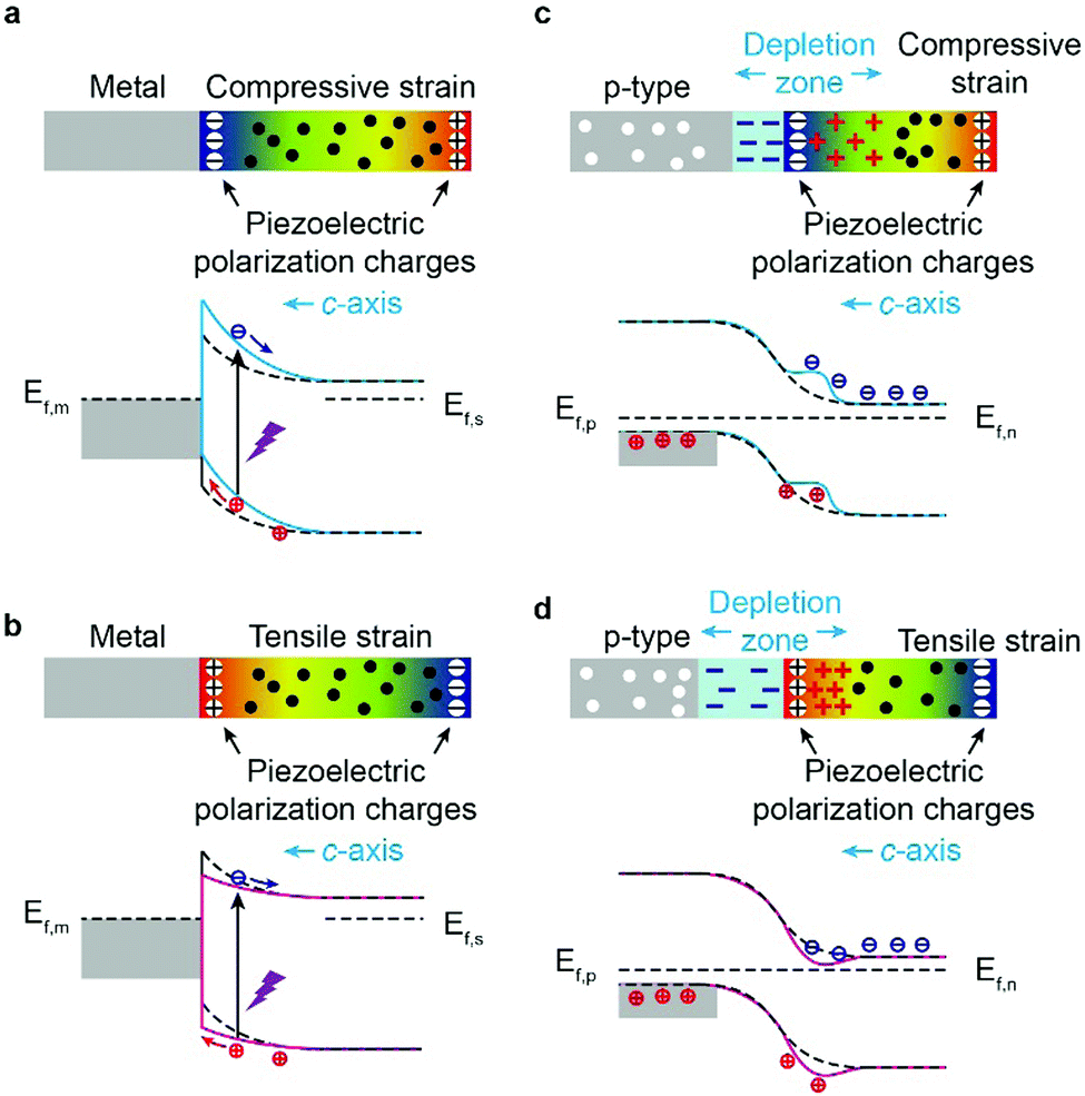 | ||
| Fig. 2 Schematic diagrams show the energy band illustrating the manipulation effect on the M–S and the p–n junction characteristics by the piezopotential. (a) Upon compressive strain, negative polarization charge is induced in the vicinity of the interface, increasing the local barrier height. (b) Upon tensile strain application, positive polarization charge is induced in the vicinity of the interface, decreasing the local barrier height. Upon strain application, negative (c) and positive (d) polarization charge is induced in the vicinity of the junction interface. The colour gradient represents the distribution of piezopotential with red indicating positive piezopotential and blue indicating negative piezopotential. Reproduced with permission.60 Copyright 2012, Wiley-VCH. | ||
2.3 Effect of piezo-charge on the p–n junction
When the p–n junction is excited by the light illumination, the electron–hole pairs generate through band-to-band light absorption.68,69 The photogenerated electrons and holes transport through the depletion region by the built-in electrical field which creates a photocurrent.70 The strain modulation on the p–n junction could be explained through the width change of the depletion zone and the band diagram deformation.71 Take a light-illuminated p–n junction with an n-type piezoelectric semiconductor as an example. Negative polarization charge will be introduced at the interface in the n-type side (Fig. 2c) when compressive strain is applied along the c-axis, and the depletion region expands and shifts toward the n-type side, decreasing the effective series resistance for charge injection to the contact and hence increasing the device current. Moreover, due to the piezo-charge, there is upward bending at the band edge to suppress electron–hole recombination and enhance the effective separation of the photogenerated carriers. Conversely, positive polarization charge is introduced when tensile strain is applied along the c-axis (Fig. 2d), where the depletion region expands and shifts toward the p-type side. This expansion of the depletion region increases the photon absorption and leads to abundant carrier generation in the p-side under illumination. However, positive polarization charge creates a dip at the band edge of the n-type semiconductor, trapping photogenerated carriers/electrons. This hampers the separation of the photogenerated electron–hole pair to a great extent and results in the decrease of the photocurrent. The p–n junction-based photodetection is modulated by static strains in the above way. The piezo-phototronic effect is an effective method to manipulate the photodetection process.2.4 Analytical solution for piezo-phototronic effect in photodetectors
The thermionic field emission (TFE) theory describes the behaviour of heavily doped semiconductor materials in which the tunnelling effect is taken into account.70 According to the TFE theory, for an n-type Schottky contact under a reverse bias voltage, the strain-free current density without illumination is described as: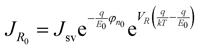 | (1) |
 | (2) |
According to previous work,73 the SBH change introduced by piezo-charge is:
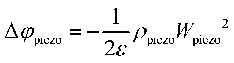 | (3) |
The SBH could also be reduced by photoexcitation besides the piezo-charge. So the total SBH change could be expressed as:
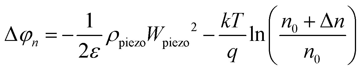 | (4) |
| φn = φn0 + Δφn | (5) |
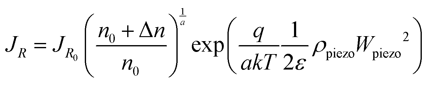 | (6) |
It is obvious that the charge carrier transport is directly related to the polarity of the applied strain (ρpiezo). The current can be enhanced or reduced by introducing positive or negative piezoelectric polarization charge at the local M–S contact, respectively.
3. Piezo-phototronic effect enhanced performance of Schottky contact photodetectors
3.1 Enhancing sensitivity of a single ZnO micro/nanowire photodetector
The charge carrier separation and transport process at the Schottky contact can be manipulated by the piezo-phototronic effect to enhance the performance of the photodetectors.34 This investigation was based on a single ZnO micro/nanowire photodetector and the experimental setup is shown schematically in Fig. 3a. The ZnO micro/nanowire was fabricated through a high-temperature thermal evaporation process.74 The Schottky contact was created at both ends of the ZnO nanowire using silver paste.75,76Fig. 3b shows the typical I–V characteristics of the device in the dark and under various UV light (372 nm) illumination intensities. The symmetric property of the I–V curves demonstrates that the Schottky contact was created at both ends of the ZnO nanowire. The I–V curves of the ZnO wire photodetector under various strains in dark conditions and under UV illumination with 2.2 × 10⁻⁵ W cm−2 excitation light intensity are shown in Fig. 3c and d, respectively. The photocurrent increases gradually with the external strain differing from −0.36% to 0.36% (Fig. 3d) at a positive bias, while the dark current remains unchanged under strain (Fig. 3c). Furthermore, the photocurrent was largely enhanced at low-level illumination using the piezo-phototronic effect (Fig. 3e). At high-level illumination, the large amount of photogenerated charge carriers can partly screen the piezopotential. By utilizing the piezo-phototronic effect, the responsivity of the device can been increased dramatically to sub-μW cm−2 (Fig. 3f).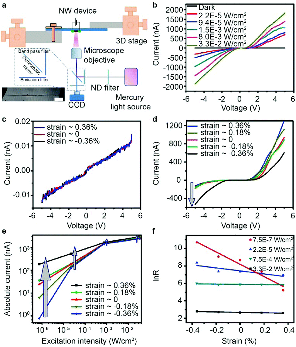 | ||
| Fig. 3 A single ZnO micro/nanowire photodetector. (a) Schematic diagram of the experimental setup. The inset in the bottom left is an optical image of the photodetector. The scale bar is 100 μm. (b) I–V characteristics of the photodetector under various UV illumination intensities (372 nm). The strain-dependent I–V curves of the ZnO wire photodetector in dark conditions (c) and under UV illumination (d) with an intensity of 2.2 × 10⁻⁵ W cm−2. (e) The change of the absolute photocurrent related to the excitation intensity under different strain. (f) Responsivity under a series of excitation intensities and external strain conditions. Reproduced with permission.34 Copyright 2010, American Chemical Society. | ||
3.2 Piezo-phototronic effect of CdSe nanowires
CdSe nanowires which possess a band gap size in the visible light region and unique optoelectronic properties have drawn much attention.78–83 Piezopotential can be created in the wurtzite structured CdSe nanowires by applying external strain. Thus, the piezo-phototronic effect is utilized to enhance the performance of the CdSe nanowire photodetector. The CdSe nanowires were grown through the vapour–liquid–solid method using Au particles as the catalyst. Fig. 4a is a scanning electron microscopy (SEM) image of CdSe nanowires together with an enlarged image. A CdSe nanowire was transferred onto a deformable PET substrate with the axis of the nanowire along the longitude direction of the substrate. Then, the two ends of the CdSe nanowire were fixed by silver paste to form Schottky contacts. Fig. 4b is the experimental setup with the optical image of the device. The light-dependent current response of the device without strain is presented in Fig. 4c, with a response and relaxation time of about 38 ms. Fig. 4d shows the strain-dependent photocurrent of devices under an illumination of 0.20 mW cm−2. The strain sensitivity under various illumination intensities is plotted in Fig. 4e. There is the same trend in the current–strain (Fig. 4d) and strain sensitivity (Fig. 4e) curves. When the applied strain increases, the response first increases and then decreases. The piezopotential increases the SBH, and this helps electrons in the junction area transport to the CdSe side, enhancing the separation of the photoexcited electron–hole pairs. So the photocurrent increases in this period (Fig. 4h). However, when the strain continues to increase, the valence CdSe band edge will be raised to a level higher than the Fermi level in the metal to form a new barrier. The separation of the photoexcited electron–hole pairs is restrained and the photocurrent decreases (Fig. 4i), which is in accordance with results in Fig. 4d and e. On the other hand, light illumination decreases the SBH (Fig. 4g), weakening the effect from the strain. So when there is illumination, the peak value of the strain modulation happens at a larger strain value as shown in Fig. 4e. For the CdSe photodetector under a certain illumination intensity, an optimum sensitivity can be obtained by modulating the applied strain.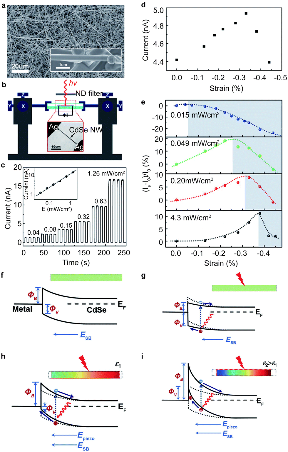 | ||
| Fig. 4 A CdSe nanowire photodetector. (a) SEM image of CdSe nanowires together with a high magnification image. (b) Schematic diagram of the experimental setup. The inset is an optical image of the CdSe photodetector. (c) Photocurrent response of the CdSe nanowire photodetector in strain-free conditions. The inset is the double-exponential fitting result of the photocurrent vs. illumination intensity. (d) The strain-dependent photocurrent of the CdSe nanowire photodetector under illumination intensity of 0.2 mW cm−2. (e) The change rate of the photocurrent under different strain with various excitation intensities. Energy band diagrams of the CdSe photodetector under (f) neither illumination nor strain, (g) only illumination, (h) illumination and slight compressive strain, and (i) illumination and large compressive strain. Reproduced with permission.77 Copyright 2012, Wiley-VCH. | ||
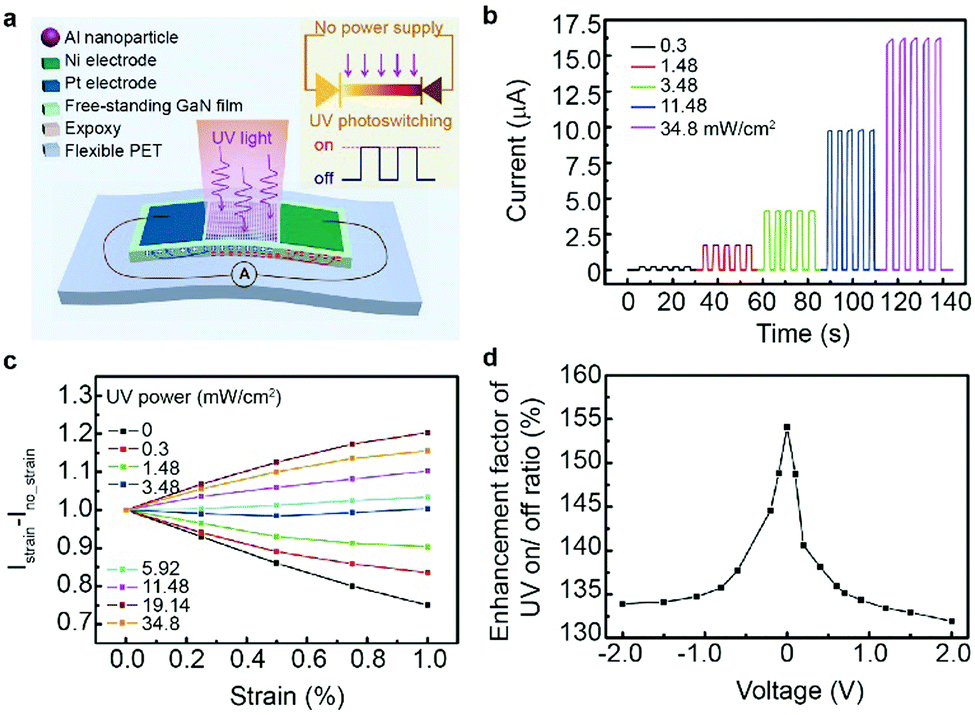
3.3 Piezo-phototronic enhanced on/off ratio of GaN film photodetector
Self-powered flexible optoelectronic sensing systems are expected to be the core of next-generation sensor networks due to their low weight, durability, and adaptability to different features of surfaces.86–88 The GaN thin film-based photodetectors with the advantages of being all-solid-state, having good chemical and thermal stability, and long lifetime are one of the candidates for the system.89,90In this work, the substrate transferring technique was used to fabricate a flexible self-powered GaN membrane-based metal–semiconductor–metal (MSM) UV photodetector, as shown in Fig. 5a. Pt and Ni were utilized to form Schottky contacts with GaN, leading to unsymmetrical photoabsorption when there is no applied voltage, which is crucial to self-powered UV detection. The self-powered photoswitching performance at 0 V bias is investigated in Fig. 5b. It exhibits a stable, fast, and wide range response to UV illumination with various intensities. It is notable that the strain modulation effect on output currents at the self-powered condition shows different trends under a variety of illumination intensities as shown in Fig. 5c. When the illumination is not strong, the SBH increase induced by the tensile strain reduces the leakage current which dominates in the current decrease. When the illumination is strong enough, more electron–hole pairs generate and they can be easily separated by the built-in electric field brought by tensile strain, leading to an increasing current. It begins to weaken at a higher intensity of UV illumination, which is due to the partial screening of piezo-charge by the large amount of photoexcited carriers. By introducing the tensile strain, the UV on/off ratio can be enhanced as shown in Fig. 5d. A peak appears at around 0 V, exhibiting a stronger strain-tuned UV on/off ratio in self-powered mode.
 | ||
| Fig. 5 Self-powered GaN film photodetector. (a) Schematic diagram of a self-powered GaN flexible film-based MSM UV photodetector. (b) Self-powered on/off switching response under different UV light illumination. (c) The ratio of device currents with strain and without strain under various illumination intensities and different strain at self-powered condition. (d) The piezo-phototronic enhancement of the UV on/off ratio under different bias voltages with a 1% tensile strain. Reproduced with permission.84 Copyright 2015, American Chemical Society. | ||
4. Piezo-phototronic effect enhanced performance of heterojunction photodetectors
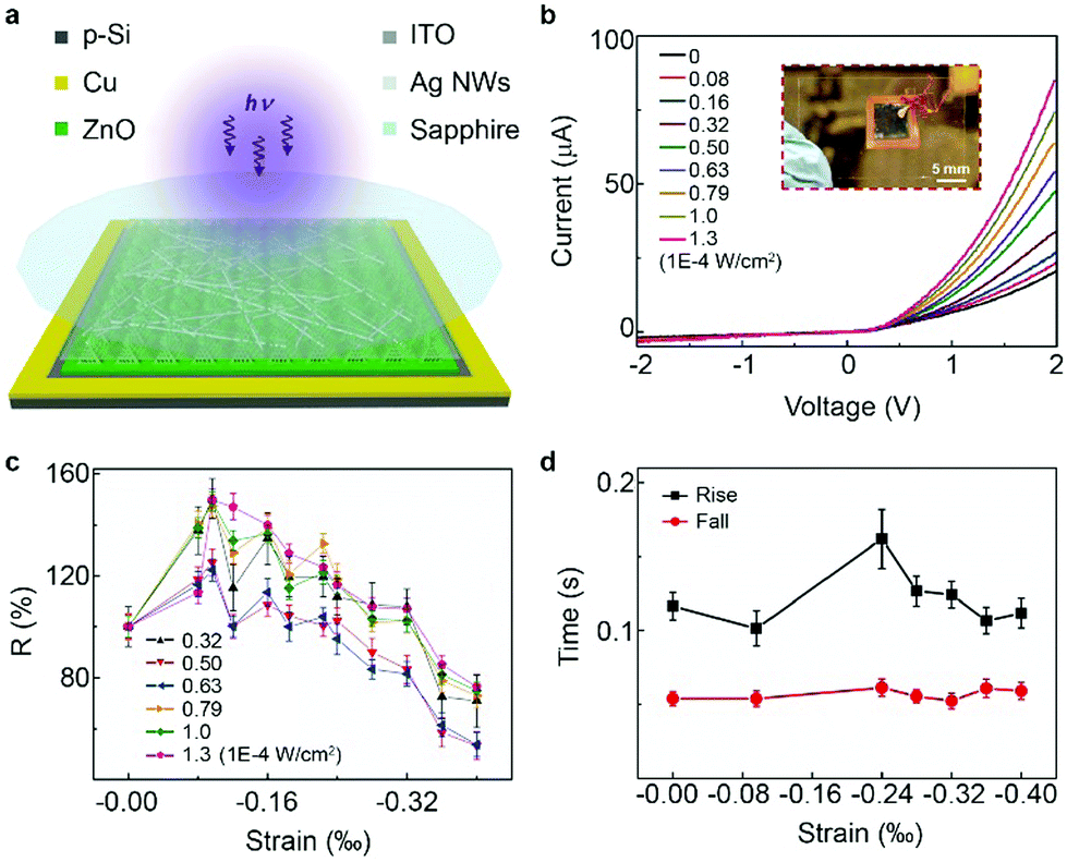
4.1 Si-based p–n junction photodetector
Silicon-based optoelectronic components play an important role in information and communication technologies because of the feasibility of integration with circuit methods.91–95 Tremendous efforts have been devoted to improve the photoresponsivity and adjustability of silicon-based nano/micro-photodetectors.96–99 Inspired by the enhanced performance by introducing the piezo-phototronic effect, a p-Si/ZnO nanowire hybridized photodetector has been fabricated.The structure design is shown in Fig. 6a. Micro-pyramids were fabricated on the p-Si wafer, and ZnO nanowires were grown on the substrate through the hydrothermal method. A thin layer of Ag nanowires was spin-coated onto the ZnO layer for better conductivity. An ITO layer and Cu layer were deposited as the top and bottom electrode respectively. The I–V curves under 442 nm laser illumination are presented in Fig. 6b together with a device image taken with a camera. To illustrate the piezo-phototronic effect on the photoresponsivity more clearly, relative changes of photoresponsivity R/R0 (R0 is the strain-free photoresponsivity) are calculated and summarized in Fig. 6c. For each illumination density, the relative change of R shows a similar trend, reaching a maximum value at a strain of −0.01%. When the illumination density was 6.3 × 10⁻⁵ W cm−2, the rise and fall time of the device under different compressive strains were obtained and are shown in Fig. 6d. No significant changes of the fall time are observed, while a minimum value of 101 ms for the rise time is observed at a strain of −0.01%, corresponding to a relative change of 87%. By introducing the piezo-phototronic effect, the photoresponsivity of the silicon-based photodetector is enhanced by 177% and the response time is shortened to 87%.
 | ||
| Fig. 6 Silicon-based p–n junction photodetector. (a) Schematic diagram of the structure of the device. (b) I–V characteristics of the photodetector under different UV illumination power densities (442 nm) with a photo of the real device. (c) Relative changes of the responsivity of the photodetector under various illumination and strain conditions. (d) The strain-dependent rise and fall time of the photodetector, under a power density of 6.3 × 10⁻⁵ W cm−2. Reproduced with permission.85 Copyright 2014, American Chemical Society. | ||
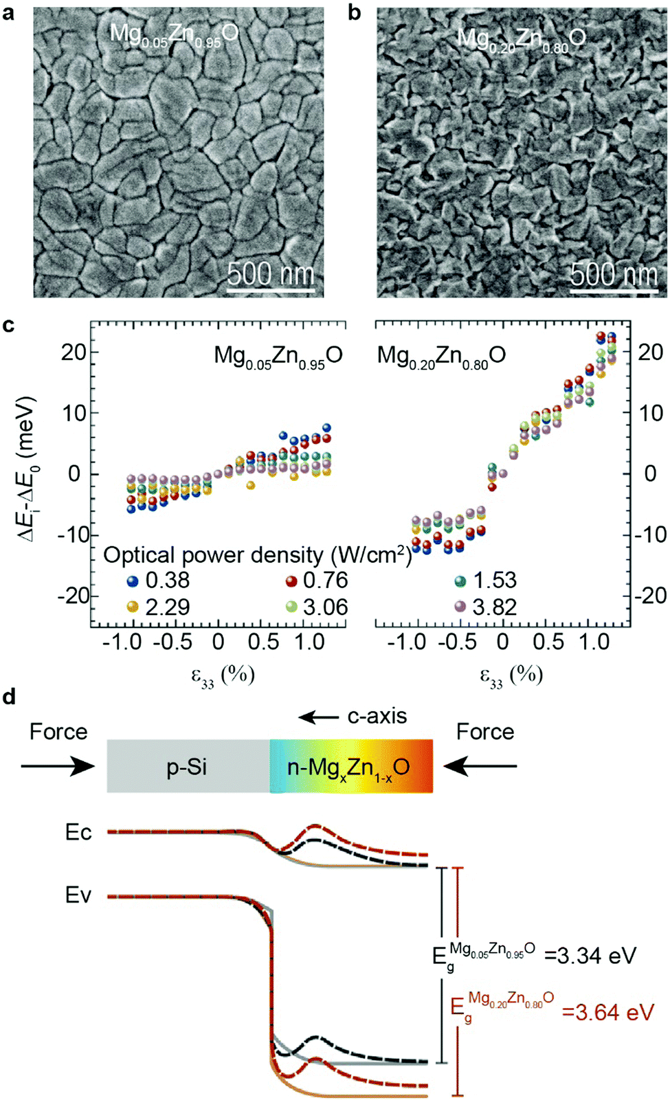
4.2 Alloying enhanced piezopotential of the p-Si/n-MgxZn1−xO photodetector
The modulation effect of the piezopotential is hindered under high illumination intensity due to the screening effect of piezo-charge by the large amount of photoexcited carriers. Tuning the doping concentration of the semiconductors can enhance the piezoelectric coefficient to reduce the screening effect.100,101 Alloying is a feasible way to enhance the piezoelectric coefficient while maintaining the crystal structure, but it has not been explored.Fig. 7a and b show the plan-view SEM images of the Mg0.05Zn0.95O and Mg0.20Zn0.80O thin films, respectively, which exhibit similar grain sizes. Fig. 7c is the dependence of the built-in potential difference (ΔEi − ΔE0) on strain under various illumination intensities, where ΔE0 and ΔEi represent the built-in potential without and with strain. The band shift by the piezo-phototronic effect is proportional to the strain when the MgZnO compound contains 5% Mg content. However, the linear trend does not appear with the higher Mg content case (20%) when the external strain is lower than −0.3%, which indicates that a flat band condition is reached at a −0.3% strain (Fig. 7d). This study demonstrates that the piezopotential of ZnO can be improved by alloying with Mg which provides an attractive approach to enhance the piezo-phototronic effect.
 | ||
| Fig. 7 Alloying enhanced piezopotential of the p-Si/n-MgxZn1−xO photodetector. Plan-view SEM images of the Mg0.05Zn0.95O (a) and Mg0.20Zn0.80O (b) thin films. (c) The changes of the built-in potential under various illumination and strain conditions for the devices with Mg0.05Zn0.95O and Mg0.20Zn0.80O. (d) Schematic band diagram of the photodetector with orange indicating the higher piezopotential of Mg0.20Zn0.80O and gray indicating the lower piezopotential of Mg0.05Zn0.95O. Reproduced with permission.102 Copyright 2014, Elsevier Ltd. | ||
4.3 Improved performance of the ZnO/spiro-MeOTAD heterojunction photodetector
Organic/inorganic hybrid photodetectors which possess unique properties with easy fabrication at low temperature, low cost, and high flexibility have drawn much attention.103–108 2,2′,7,7′-Tetrakis(N,N-di-p-methoxyphenylamine) 9,9′-spirobifluorene (spiro-MeOTAD) is a common hole conductor with both a non-hazardous property and efficient hole regeneration capability, thus it can be used in photodetectors.109Fig. 8a shows the structure of the ZnO/spiro-MeOTAD heterojunction photodetector. The ZnO film was deposited on the commercial flexible ITO/PET substrate. Spiro-MeOTAD solution was spin-coated onto the ZnO film. The Au film was thermally evaporated onto the as-fabricated device as the top electrode. Fig. 8b shows the I–V curves under different strain with 1 mW cm−2 UV illumination, and the inset is a schematic of the testing process. The photocurrent under different strain in the self-powered condition is shown in Fig. 8c. The responsivity and detectivity are also investigated to illustrate the strain modulation effect of the device, as shown in Fig. 8d. All of the photocurrent, responsivity, and detectivity increase gradually when the strain changes from compressive strain to the tensile strain. This work demonstrates that strain engineering is a feasible way to enhance the performance of the ZnO/spiro-MeOTAD heterojunction photodetector.
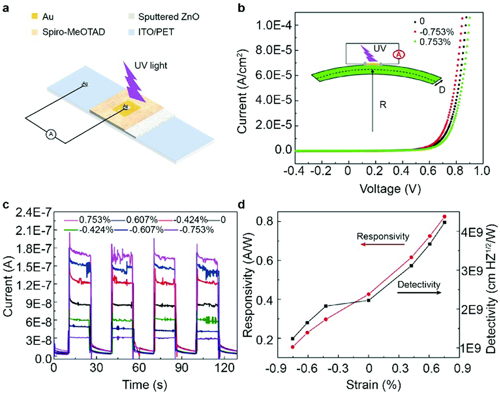 | ||
| Fig. 8 Self-powered ZnO/spiro-OMeTAD heterojunction UV photodetector. (a) Schematic diagram of the structure of the photodetector. (b) I–V characteristics of the photodetector under tensile strain, compressive strain, and strain-free conditions. The inset is a schematic of the experimental setup. (c) Photocurrent response of the device under various strain at self-powered condition. (d) Responsivity and detectivity under various applied strains. Reproduced with permission.110 Copyright 2016, American Chemical Society. | ||
4.4 Enhanced visible and ultraviolet photodetection using the ZnO–CdS core–shell structure
A schematic configuration of a ZnO–CdS core–shell nanowire is shown in Fig. 9a. The ZnO wires were synthesized by the chemical vapour deposition process, followed by the growth of a CdS nanowires array by the hydrothermal method. Fig. 9b is a scanning transmission electron microscopy (STEM) image of the ZnO–CdS nanowire. The results of energy dispersive X-ray (EDX) analysis across the nanowire along the red line in Fig. 9b are presented in Fig. 9c. Zn is located in the core while Cd and S distribute at the shell which proves that the ZnO nanowire is wrapped by CdS to form the core–shell structure.
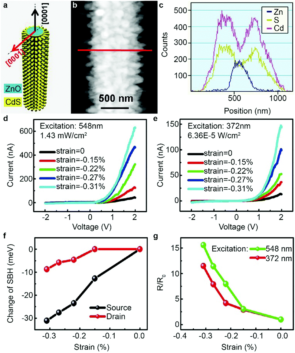 | ||
| Fig. 9 A ZnO–CdS core–shell photodetector. (a) Schematic diagram of the structure of the ZnO/CdS wire. (b) STEM image of a ZnO–CdS wire. (c) The result of the EDX analysis. (d and e) I–V characteristics of the device under varying compressive strain, excited by green light (d) and UV light (e). (f) Change of the SBH of the source and drain sides under varying compressive strain. (g) Relative responsivity under compressive strain, where R0 is the responsivity without strain. Reproduced with permission.118 Copyright 2012, American Chemical Society. | ||
The I–V characteristics of the device under various illumination and strain conditions are shown in Fig. 9d and e. The current of the photodetector at a positive bias increased gradually with applied compressive strain increasing under both green light and UV light illumination. Fig. 9f shows the changes of the SBH at the two ends of the wire with strains at a bias of 2 V. Both SBHs exhibit a similar trend with the strain. The asymmetric decreasing tendency indicates the participation of the piezopotential. The relative changes of photoresponsivity are calculated and summarized in Fig. 9g. The responsivity is enhanced by more than ten-fold when the strain is −0.4% compared to the strain-free nanowire.
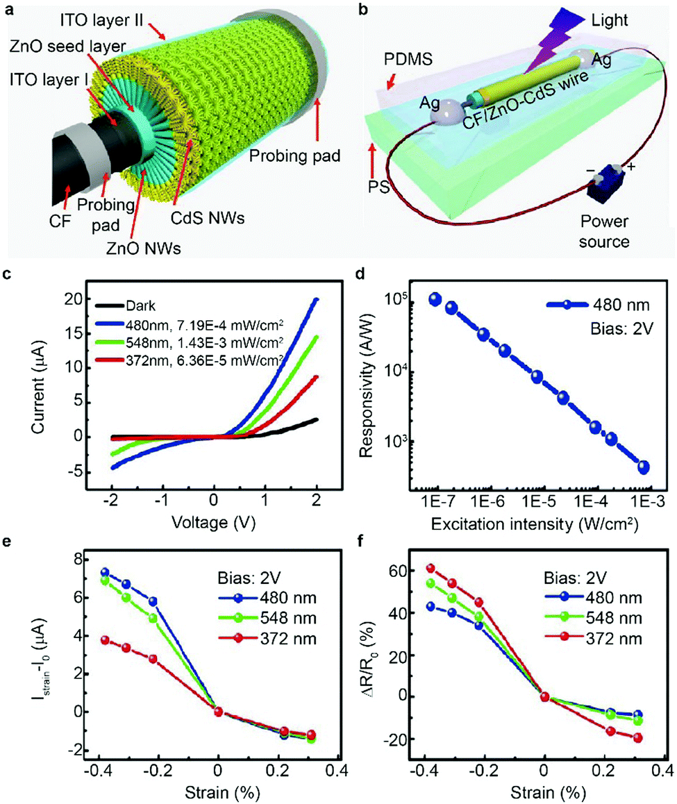 | ||
| Fig. 10 A CF/ZnO–CdS double-shell wire-based photodetector. (a and b) Schematic diagrams of the photodetector structure and the experimental setup. (c) I–V characteristics of the device excited by UV (372 nm), blue (480 nm), and green (548 nm) light illumination. (d) Responsivity of the device excited by blue light illumination. (e and f) Change of current and responsivity under different illumination and strain conditions. Reproduced with permission.119 Copyright 2013, American Chemical Society. | ||
The I–V curves in a dark environment were measured and the conditions under three different wavelengths of light illumination are also presented in Fig. 10c. Fig. 10d is the photon responsivity with the increasing excitation intensity under blue light (480 nm) illumination. The changes of photocurrent at 2 V bias voltage under different strains are plotted in Fig. 10e, which clearly demonstrate that the photocurrent monotonously increases with compressive strain increasing while tensile strain contributes to a current decrease. The responsivity of the photodetector exhibits the same tendency with the photocurrent under both compressive and tensile strain conditions (Fig. 10f).
Fig. 11a shows a structure schematic and corresponding energy band diagrams of a strain-free device. When the CF is under tensile strain along the axial direction, corresponding compressive strain is created in the ZnO nanowire, inducing negative piezo-charge in the ZnO/CdS interface. The negative piezo-charge makes a higher barrier at the band edge, and hampers the photogenerated electron transport from the excited ZnO and traps photogenerated holes from the excited CdS (Fig. 11b), leading to the decrease of photocurrent and responsivity. Conversely, when compressive strain along the wire introduces positive piezo-charge at the interface, and the barrier height decreases (Fig. 11c), this enhances the photogenerated electron transport from the excited ZnO, and in the excited CdS, the trapping of photogenerated holes was restrained, thus enhancing the performance. The direct integration of branched ZnO–CdS double-shell nanowires and CF not only enables the 3D nanostructure array to sense the light but also introduces a flexible substrate with good stability and the performance can be enhanced by introducing the piezo-phototronic effect.
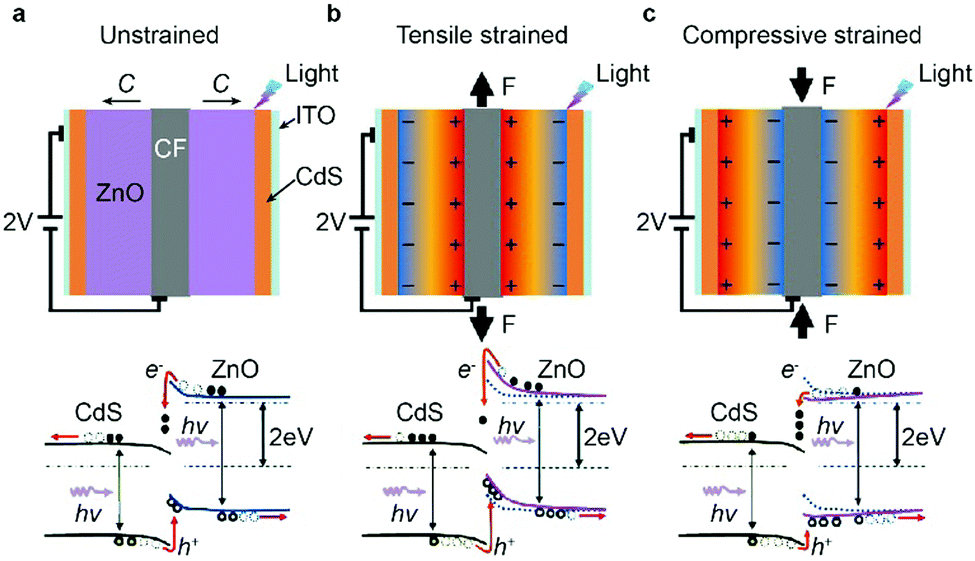 | ||
| Fig. 11 Schematic of the piezopotential distribution and the corresponding energy band diagrams of the CF/ZnO–CdS wire photodetector under (a) light illumination, (b) light illumination and tensile strain, and (c) light illumination and compressive strain. Reproduced with permission.119 Copyright 2013, American Chemical Society. | ||
As Fig. 12a shows, the UV/visible photodetector has been integrated with an optical fiber directly. ZnO/CdS nanowire heterojunctions are synthesized through a two-step hydrothermal method which is same as the carbon fiber ZnO/CdS double-shell photodetector mentioned above. There are two working modes for the device: axial and off-axial illumination mode (Fig. 12b). For the axial illumination mode, a 325 nm laser is focused at the end of the OF as UV stimulus. The optoelectronic behaviour of the device under 325 nm axial illumination mode is shown in Fig. 12c, signifying an obvious enhancement in the photocurrent with the applied strain increasing. The inset is the photocurrent under off-axial illumination to compare with the axial mode. The current values in the two modes are of the same order, while the excited power density of the axial illumination is about 10% of that employed for the off-axial mode. The relative changes of the photoresponsivity with strain are calculated and presented in Fig. 12d. When there is a larger external strain or stronger incident light is applied, the relative change increases. The piezo-phototronic effect enhanced performance under 532 nm off-axial illumination was studied in a similar manner, and the results are summarized in Fig. 12e and f. These results demonstrate the capability of the device in visible detection. The piezo-phototronic effect enhanced OF/ZnO–CdS hybridized photodetector can be directly integrated with an optical communication system by the fiber welding technology, which provides a possible solution to avoid energy losses.
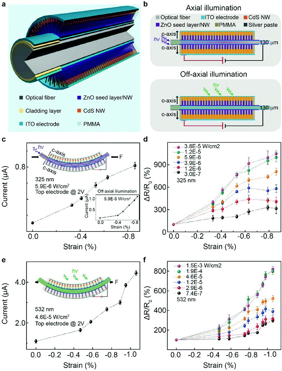 | ||
| Fig. 12 A photodetector based on optical fiber ZnO–CdS hybridized structures. (a) Schematic illustration of the optical fiber ZnO–CdS hybridized structure. (b) Schematic demonstration of the axial illumination and off-axial illumination mode. (c) Strain-dependent photocurrent of the device in the axial illumination mode (325 nm) with the schematic experimental setup. The bottom right is the I-strain curve in the off-axial illumination mode (325 nm). (e) I-strain curve in the off-axial illumination mode (532 nm). (d and f) Relative changes of responsivity of the device operating in axial illumination (d) and off-axial illumination (f) modes under different illumination and strain conditions. Reproduced with permission.126 Copyright 2015, Wiley-VCH. | ||
4.5 Three-dimensional core–shell nanowire array photodetector
Compared with the single nanowire devices, the three-dimensional (3D) core–shell nanowire array devices possess unique advantages, like simultaneous multichannel charge transport, large surface area, and increased light absorption.127–131 Type-II heterostructures can extend the photoresponse spectral range to the longer wavelength which is dominated by the lower band gap component. Both the ZnO/ZnS and CdSe/ZnTe core–shell nanowires which have type II alignment exhibit an efficient broad band UV/visible photoresponse.132,133 The piezoelectric effect of ZnO and CdSe makes the two types of core–shell structures excellent candidates for piezo-phototronic effect devices.Fig. 13a shows the structure of the 3D photodetector. The ZnO/ZnS core–shell structure was fabricated through a two-step method. First, the ZnO nanowire array was synthesized on the substrate through the chemical vapor deposition process and then the shell materials were deposited on the ZnO array through the pulsed laser deposition system. A polyester grating coated with a thin layer of Ag was positioned on the top of the core–shell nanowire array as the top electrode. The SEM images of the ZnO nanowire array and the fabricated ZnO/ZnS core–shell nanowire array are shown in Fig. 13b. Few ZnS particles were deposited on the surface of the nanowire array. The photocurrent of the ZnO/ZnS core–shell device under UV, blue, and green illumination and various strain conditions is summarized in Fig. 13c. Fig. 13d shows the relative change of the responsivity of the device under different illumination and strain conditions. Both the photocurrent and responsivity increase monotonously with the compressive strain enhancing. This work expands the application of the piezo-phototronic effect to a 3D core–shell nanowire array photodetector.
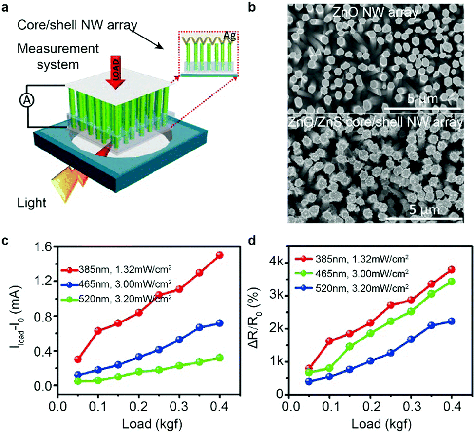 | ||
| Fig. 13 Three-dimensional photodetector based on a ZnO–ZnS core–shell nanowire array. (a) Schematic diagram of the device structure and experimental setup. (b) SEM image of the ZnO nanowire array (top) and ZnO/ZnS (bottom) core/shell nanowire array. (c and d) Absolute current (c) and relative change of responsivity (d) of the photodetector based on the ZnO/ZnS core–shell nanowire array with compressive load under UV (385 nm), blue (465 nm), and green (520 nm) illumination. Reproduced with permission.134 Copyright 2015, American Chemical Society. | ||
5. Piezo-phototronic effect enhanced photodetector array
Tremendous efforts have been devoted to making highly photoresponsive large-scale photodetectors, as there is a rapidly growing demand for good-performance photosensing devices. A fast response time and adequate spatial resolution are pursued.135–138 Developing nanowire photodetectors into an integrated array configuration is proposed as a promising solution. The structure design of the proposed UV photodetector array is presented in Fig. 14a, and the inset is an optical image of the as-fabricated device. Each device consists of 32 × 40 pixels which are made up of ZnO NWs. The ZnO nanowire array was grown on the ITO layers through the hydrothermal method. Each nanowire bunch is a pixel of the UV photodetector array. Then the space among the nanowire bunches was filled with SU-8 photoresist. An ITO/Au electrode layer was deposited, crossing equally with the bottom electrode layer. The photoresponse of a single pixel under various illumination intensities is shown in Fig. 14b. A 62 ms response time was obtained at the rising edge with the UV illumination intensity of 3.949 mW cm−2. Fig. 14c shows the photoresponsivity of a single pixel under different UV illumination. To characterise all the pixels in the photodetector array at the same time, a multichannel testing system was employed (Fig. 14d). The illumination is applied on the device through a mask on which there is a C-shape to let the light go through, and when the light intensity increases, a clear C-shape output is derived.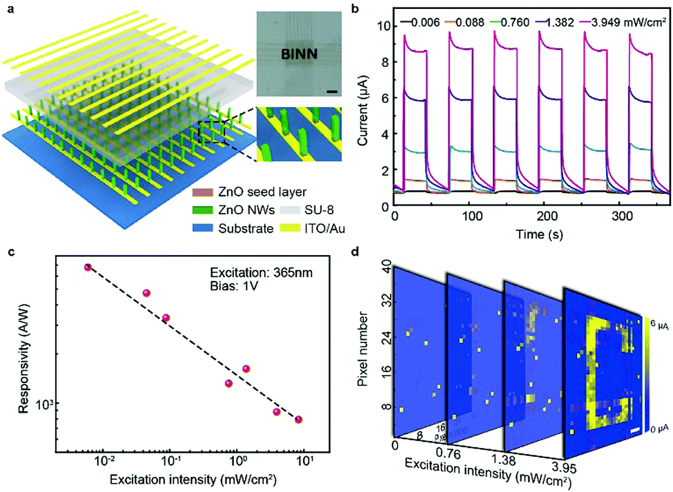 | ||
| Fig. 14 A Schottky photodetector array for light distribution imaging. (a) Schematic demonstration of the photodetector array structure together with an optical image of the as-fabricated device. The scale bar is 1 mm. (b) Photoresponse under 365 nm illumination with different intensities. (c) UV illumination intensity dependence of responsivity. (d) The photocurrent of the UV photodetector array to image the UV illumination distribution. The scale bar is 500 μm. Reproduced with permission.30 Copyright 2015, Wiley-VCH. | ||
External strain was introduced to optimize the UV sensing performance of the photodetector array. A strain modulation process was carried out on a single pixel first. The corresponding I–V curves are summarized in Fig. 15a under no illumination. When 1.38 mW cm−2 UV illumination was applied, the output currents of the entire device were measured both strain-free (Fig. 15b) and under 40.83 MPa pressure (Fig. 15c). Clearly, the UV sensing performance was enhanced by the piezo-phototronic effect, and a clearer C-shape output (Fig. 15c) was presented by the device indicating the higher photoresponsivity and sensitivity. Furthermore, with the help of 40.83 MPa pressure, the illumination distribution was successfully imaged by the photodetector array when the illumination intensity is 1.38 mW cm−2, which could only be achieved with at least 3.95 mW cm−2 at strain-free conditions (Fig. 14d). When we subtracted the data in Fig. 15b from Fig. 15c, the C-shape became more obvious (Fig. 15d). The enhancement of the total photocurrent by applying strain is summarized in Fig. 15e, together with the image of the illumination distribution under different strain. This work provides a feasible method to fabricate high-performance large-scale photodetectors through integrating NW photodetectors into an array configuration. The piezo-phototronic effect enhanced UV photodetector array device may have prospective applications in multifunctional optoelectronics, adaptive optical systems, and optical communication.
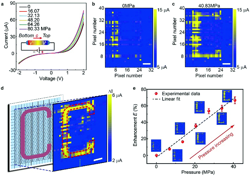 | ||
| Fig. 15 The enhanced performance of the photodetector array by introducing the piezo-phototronic effect. (a) I–V curves of a single ZnO nanowire pixel under various compressive strain. (b and c) The distribution of the UV illumination with an excited light intensity of 1.38 mW cm−2 at strain-free (b) and 40.38 MPa pressure (c) conditions. (d) Photocurrent difference between the strain-free (b) and strain (c) conditions. (e) The applied pressure dependence of the enhancement factor E together with the corresponding image of illumination distribution at an excited light intensity of 1.38 mW cm−2. Reproduced with permission.30 Copyright 2015, Wiley-VCH. | ||
6. Summary and outlook
In summary, we have presented the recent progresses in wurtzite structured material photodetector design and performance enhanced by the piezo-phototronic effect. By introducing the piezopotential upon straining, the optoelectronic processes are modulated. Newly found fundamental phenomena and recently developed device performance as a result of the piezo-phototronic effect have been demonstrated, from a single nanowire device to photodetector arrays for illumination imaging. The material investigation has been carried out for both organic materials and alloys, significantly improving the understanding of piezo-phototronics. It is promising that this technology will bring revolution to energy harvesting, human electronics interfacing display, multifunctional systems, and so on.Acknowledgements
The authors are thankful for support from the “Thousand Talents” program of China for pioneering researchers and innovative teams, the support of national key R&D project from Minister of Science and Technology, China (2016YFA0202703), National Natural Science Foundation of China (No. 51622205, 61675027, 61405040, 51432005, 61505010 and 51502018), Beijing City Committee of Science and Technology (Z151100003315010), Beijing Natural Science Foundation (2164076), and the President Funding of the Chinese Academy of Sciences.Notes and references
- L. Kou, T. Q. Huang, B. N. Zheng, Y. Han, X. L. Zhao, K. Gopalsamy, H. Y. Sun and C. Gao, Nat. Commun., 2014, 5, 3754 CrossRef CAS PubMed.
- D. Son, J. Lee, S. Qiao, R. Ghaffari, J. Kim, J. E. Lee, C. Song, S. J. Kim, D. J. Lee, S. W. Jun, S. Yang, M. Park, J. Shin, K. Do, M. Lee, K. Kang, C. S. Hwang, N. S. Lu, T. Hyeon and D. H. Kim, Nat. Nanotechnol., 2014, 9, 397–404 CrossRef CAS PubMed.
- Y. Bae, S. Fukushima, A. Harada and K. Kataoka, Angew. Chem., Int. Ed., 2003, 42, 4640–4643 CrossRef CAS PubMed.
- I. F. Akyildiz, W. Su, Y. Sankarasubramaniam and E. Cayirci, Comput. Netw., 2002, 38, 393–422 CrossRef.
- K. T. V. Grattan and T. Sun, Sens. Actuators, A, 2000, 82, 40–61 CrossRef CAS.
- C. H. Dong, L. He, Y. F. Xiao, V. R. Gaddam, S. K. Ozdemir, Z. F. Han, G. C. Guo and L. Yang, Appl. Phys. Lett., 2009, 94, 231119 CrossRef.
- C. Wang, D. Hwang, Z. B. Yu, K. Takei, J. Park, T. Chen, B. W. Ma and A. Javey, Nat. Mater., 2013, 12, 899–904 CrossRef CAS PubMed.
- C. F. Pan, L. Dong, G. Zhu, S. M. Niu, R. M. Yu, Q. Yang, Y. Liu and Z. L. Wang, Nat. Photonics, 2013, 7, 752–758 CrossRef CAS.
- X. D. Wang, H. L. Zhang, R. M. Yu, L. Dong, D. F. Peng, A. H. Zhang, Y. Zhang, H. Liu, C. F. Pan and Z. L. Wang, Adv. Mater., 2015, 27, 2324–2331 CrossRef CAS PubMed.
- X. D. Wang, H. L. Zhang, L. Dong, X. Han, W. M. Du, J. Y. Zhai, C. F. Pan and Z. L. Wang, Adv. Mater., 2016, 28, 2896–2903 CrossRef CAS PubMed.
- X. L. Zhao, Q. L. Hua, R. M. Yu, Y. Zhang and C. F. Pan, Adv. Electron. Mater., 2015, 1, 1500142 CrossRef.
- Q. L. Hua, H. T. Liu, J. Zhao, D. F. Peng, X. N. Yang, L. Gu and C. F. Pan, Adv. Electron. Mater., 2016, 2, 1600093 CrossRef.
- J. A. Rogers, T. Someya and Y. G. Huang, Science, 2010, 327, 1603–1607 CrossRef CAS PubMed.
- G. Konstantatos and E. H. Sargent, Nat. Nanotechnol., 2010, 5, 391–400 CrossRef CAS PubMed.
- G. Konstantatos, I. Howard, A. Fischer, S. Hoogland, J. Clifford, E. Klem, L. Levina and E. H. Sargent, Nature, 2006, 442, 180–183 CrossRef CAS PubMed.
- H. Kind, H. Q. Yan, B. Messer, M. Law and P. D. Yang, Adv. Mater., 2002, 14, 158–160 CrossRef CAS.
- S. A. McDonald, G. Konstantatos, S. G. Zhang, P. W. Cyr, E. J. D. Klem, L. Levina and E. H. Sargent, Nat. Mater., 2005, 4, 138–142 CrossRef CAS PubMed.
- J. Qi, X. K. Zhou, D. Z. Yang, W. Q. Qiao, D. G. Ma and Z. Y. Wang, Adv. Funct. Mater., 2014, 24, 7605–7612 CrossRef CAS.
- D. Ruh, P. Reith, S. Sherman, M. Theodor, J. Ruhhammer, A. Seifert and H. Zappe, Adv. Mater., 2014, 26, 1706–1710 CrossRef CAS PubMed.
- M. M. Russew and S. Hecht, Adv. Mater., 2010, 22, 3348–3360 CrossRef CAS PubMed.
- Y. B. Li, T. Tokizono, M. Y. Liao, M. A. Zhong, Y. Koide, I. Yamada and J. J. Delaunay, Adv. Funct. Mater., 2010, 20, 3972–3978 CrossRef CAS.
- X. Liu, L. L. Gu, Q. P. Zhang, J. Y. Wu, Y. Z. Long and Z. Y. Fan, Nat. Commun., 2014, 5, 4007 CAS.
- M. Engel, M. Steiner and P. Avouris, Nano Lett., 2014, 14, 6414–6417 CrossRef CAS PubMed.
- O. Lopez-Sanchez, D. Lembke, M. Kayci, A. Radenovic and A. Kis, Nat. Nanotechnol., 2013, 8, 497–501 CrossRef CAS PubMed.
- M. A. Green, Prog. Photovoltaics, 2001, 9, 123–135 CAS.
- A. J. Nozik, M. C. Beard, J. M. Luther, M. Law, R. J. Ellingson and J. C. Johnson, Chem. Rev., 2010, 110, 6873–6890 CrossRef CAS PubMed.
- A. Rogalski, J. Antoszewski and L. Faraone, J. Appl. Phys., 2009, 105, 091101 CrossRef.
- X. Q. Liu, L. Jiang, X. M. Zou, X. H. Xiao, S. S. Guo, C. Z. Jiang, X. Liu, Z. Y. Fan, W. D. Hu, X. S. Chen, W. Lu, W. P. Hu and L. Liao, Adv. Mater., 2014, 26, 2919–2924 CrossRef CAS PubMed.
- J. Zhou, Y. D. Gu, Y. F. Hu, W. J. Mai, P. H. Yeh, G. Bao, A. K. Sood, D. L. Polla and Z. L. Wang, Appl. Phys. Lett., 2009, 94, 191103 CrossRef PubMed.
- X. Han, W. M. Du, R. M. Yu, C. F. Pan and Z. L. Wang, Adv. Mater., 2015, 27, 7963–7969 CrossRef CAS PubMed.
- Z. Zhang, Q. L. Liao, Y. H. Yu, X. D. Wang and Y. Zhang, Nano Energy, 2014, 9, 237–244 CrossRef CAS.
- Y. F. Hu, Y. Zhang, Y. L. Chang, R. L. Snyder and Z. L. Wang, ACS Nano, 2010, 4, 4220–4224 CrossRef CAS PubMed.
- Q. Yang, W. H. Wang, S. Xu and Z. L. Wang, Nano Lett., 2011, 11, 4012–4017 CrossRef CAS PubMed.
- Q. Yang, X. Guo, W. H. Wang, Y. Zhang, S. Xu, D. H. Lien and Z. L. Wang, ACS Nano, 2010, 4, 6285–6291 CrossRef CAS PubMed.
- Z. L. Wang and W. Z. Wu, Natl. Sci. Rev., 2014, 1, 62–90 CrossRef.
- R. R. Bao, C. F. Wang, L. Dong, R. M. Yu, K. Zhao, Z. L. Wang and C. F. Pan, Adv. Funct. Mater., 2015, 25, 2884–2891 CrossRef CAS.
- C. F. Pan, M. X. Chen, R. M. Yu, Q. Yang, Y. F. Hu, Y. Zhang and Z. L. Wang, Adv. Mater., 2016, 28, 1535–1552 CrossRef CAS PubMed.
- R. R. Zhou, G. F. Hu, R. M. Yu, C. F. Pan and Z. L. Wang, Nano Energy, 2015, 12, 588–596 CrossRef CAS.
- C. F. Wang, R. R. Ba, K. Zhao, T. P. Zhang, L. Dong and C. F. Pan, Nano Energy, 2015, 14, 364–371 CrossRef CAS.
- R. M. Yu, S. M. Niu, C. F. Pan and Z. L. Wang, Nano Energy, 2015, 14, 312–339 CrossRef CAS.
- R. M. Yu, X. F. Wang, W. Z. Wu, C. F. Pan, Y. Bando, N. Fukata, Y. F. Hu, W. B. Peng, Y. Ding and Z. L. Wang, Adv. Funct. Mater., 2015, 25, 5277–5284 CrossRef CAS.
- Y. Liu, Y. Zhang, Q. Yang, S. M. Niu and Z. L. Wang, Nano Energy, 2015, 14, 257–275 CrossRef CAS.
- M. X. Chen, C. F. Pan, T. P. Zhang, X. Y. Li, R. R. Liang and Z. L. Wang, ACS Nano, 2016, 10, 6074–6079 CrossRef CAS PubMed.
- W. Z. Wu, X. N. Wen and Z. L. Wang, Science, 2013, 340, 952–957 CrossRef CAS PubMed.
- W. Z. Wu, L. Wang, Y. L. Li, F. Zhang, L. Lin, S. M. Niu, D. Chenet, X. Zhang, Y. F. Hao, T. F. Heinz, J. Hone and Z. L. Wang, Nature, 2014, 514, 470–474 CrossRef CAS PubMed.
- J. J. Qi, Y. W. Lan, A. Z. Stieg, J. H. Chen, Y. L. Zhong, L. J. Li, C. D. Chen, Y. Zhang and K. L. Wang, Nat. Commun., 2015, 6, 7430 CrossRef CAS PubMed.
- X. Y. Li, M. X. Chen, R. M. Yu, T. P. Zhang, D. S. Song, R. R. Liang, Q. L. Zhang, S. B. Cheng, L. Dong, A. L. Pan, Z. L. Wang, J. Zhu and C. F. Pan, Adv. Mater., 2015, 27, 4447–4453 CrossRef CAS PubMed.
- Q. L. Liao, M. Y. Liang, Z. Zhang, G. J. Zhang and Y. Zhang, Nano Res., 2015, 8, 3772–3779 CrossRef CAS.
- P. Lin, X. Chen, X. Q. Yan, Z. Zhang, H. G. Yuan, P. F. Li, Y. G. Zhao and Y. Zhang, Nano Res., 2014, 7, 860–868 CrossRef CAS.
- R. R. Bao, C. F. Wang, L. Dong, C. Y. Shen, K. Zhao and C. F. Pan, Nanoscale, 2016, 8, 8078–8082 RSC.
- G. F. Hu, R. R. Zhou, R. M. Yu, L. Dong, C. F. Pan and Z. L. Wang, Nano Res., 2014, 7, 1083–1091 CrossRef CAS.
- G. F. Hu, W. X. Guo, R. M. Yu, X. N. Yang, R. R. Zhou, C. F. Pan and Z. L. Wang, Nano Energy, 2016, 23, 27–33 CrossRef CAS.
- Z. L. Wang and J. H. Song, Science, 2006, 312, 242–246 CrossRef CAS PubMed.
- Z. L. Wang, Adv. Funct. Mater., 2008, 18, 3553–3567 CrossRef CAS.
- Z. L. Wang, Mater. Sci. Eng., R, 2009, 64, 33–71 CrossRef.
- Z. L. Wang, R. S. Yang, J. Zhou, Y. Qin, C. Xu, Y. F. Hu and S. Xu, Mater. Sci. Eng., R, 2010, 70, 320–329 CrossRef.
- Z. L. Wang, Nano Today, 2010, 5, 540–552 CrossRef CAS.
- C. K. Jeong, K. I. Park, J. Ryu, G. T. Hwang and K. J. Lee, Adv. Funct. Mater., 2014, 24, 2620–2629 CrossRef CAS.
- K. Momeni, G. M. Odegard and R. S. Yassar, J. Appl. Phys., 2010, 108, 114303 CrossRef.
- Z. L. Wang, Adv. Mater., 2012, 24, 4632–4646 CrossRef CAS PubMed.
- Z. Y. Gao, J. Zhou, Y. D. Gu, P. Fei, Y. Hao, G. Bao and Z. L. Wang, J. Appl. Phys., 2009, 105, 113707 CrossRef PubMed.
- L. J. Brillson and Y. C. Lu, J. Appl. Phys., 2011, 109, 121301 CrossRef.
- D. K. Ferry, R. Akis, A. Cummings, M. J. Gilbertl and S. M. Ramey, 2006 International Conference on Nanoscience and Nanotechnology, 2006, vol. 1 and 2, pp. 114–119 Search PubMed.
- Z. M. Liao, K. J. Liu, J. M. Zhang, J. Xu and D. P. Yu, Phys. Lett. A, 2007, 367, 207–210 CrossRef CAS.
- S. Liang, H. Sheng, Y. Liu, Z. Huo, Y. Lu and H. Shen, J. Cryst. Growth, 2001, 225, 110–113 CrossRef CAS.
- M. A. Khan, J. N. Kuznia, D. T. Olson, M. Blasingame and A. R. Bhattarai, Appl. Phys. Lett., 1993, 63, 2455–2456 CrossRef CAS.
- F. A. Padovani and R. Stratton, Solid-State Electron., 1966, 9, 695–707 CrossRef.
- E. Monroy, E. Munoz, F. J. Sanchez, F. Calle, E. Calleja, B. Beaumont, P. Gibart, J. A. Munoz and F. Cusso, Semicond. Sci. Technol., 1998, 13, 1042–1046 CrossRef CAS.
- Q. Chen, M. A. Khan, C. J. Sun and J. W. Yang, Electron. Lett., 1995, 31, 1781–1782 CrossRef CAS.
- S. M. Sze, CC/Eng. Tech. Appl. Sci., 1982, 28 Search PubMed.
- Y. Liu, S. M. Niu, Q. Yang, B. D. B. Klein, Y. S. Zhou and Z. L. Wang, Adv. Mater., 2014, 26, 7209–7216 CrossRef CAS PubMed.
- Z. Y. Zhang, K. Yao, Y. Liu, C. H. Jin, X. L. Liang, Q. Chen and L. M. Peng, Adv. Funct. Mater., 2007, 17, 2478–2489 CrossRef CAS.
- Y. Zhang, Y. Liu and Z. L. Wang, Adv. Mater., 2011, 23, 3004–3013 CrossRef CAS PubMed.
- Z. W. Pan, Z. R. Dai and Z. L. Wang, Science, 2001, 291, 1947–1949 CrossRef CAS PubMed.
- J. Zhou, P. Fei, Y. D. Gu, W. J. Mai, Y. F. Gao, R. Yang, G. Bao and Z. L. Wang, Nano Lett., 2008, 8, 3973–3977 CrossRef CAS PubMed.
- J. Zhou, Y. D. Gu, P. Fei, W. J. Mai, Y. F. Gao, R. S. Yang, G. Bao and Z. L. Wang, Nano Lett., 2008, 8, 3035–3040 CrossRef CAS PubMed.
- L. Dong, S. M. Niu, C. F. Pan, R. M. Yu, Y. Zhang and Z. L. Wang, Adv. Mater., 2012, 24, 5470–5475 CrossRef CAS PubMed.
- J. Debaets, J. Vanfleteren, I. Derycke, J. Doutreloigne, A. Vancalster and P. Devisschere, IEEE Trans. Electron Devices, 1990, 37, 636–639 CrossRef CAS.
- M. Achermann, M. A. Petruska, S. Kos, D. L. Smith, D. D. Koleske and V. I. Klimov, Nature, 2004, 429, 642–646 CrossRef CAS PubMed.
- I. Gur, N. A. Fromer, M. L. Geier and A. P. Alivisatos, Science, 2005, 310, 462–465 CrossRef CAS PubMed.
- T. Uematsu, J. Kimura and Y. Yamaguchi, Nanotechnology, 2004, 15, 822–827 CrossRef CAS.
- X. J. Ji, J. Y. Zheng, J. M. Xu, V. K. Rastogi, T. C. Cheng, J. J. DeFrank and R. M. Leblanc, J. Phys. Chem. B, 2005, 109, 3793–3799 CrossRef CAS PubMed.
- Y. Xing, Q. Chaudry, C. Shen, K. Y. Kong, H. E. Zhau, L. WChung, J. A. Petros, R. M. O'Regan, M. V. Yezhelyev, J. W. Simons, M. D. Wang and S. Nie, Nat. Protoc., 2007, 2, 1152–1165 CrossRef CAS PubMed.
- M. Z. Peng, Y. D. Liu, A. F. Yu, Y. Zhang, C. H. Liu, J. Y. Liu, W. Wu, K. Zhang, X. Q. Shi, J. Z. Kou, J. Y. Zhai and Z. L. Wang, ACS Nano, 2016, 10, 1572–1579 CrossRef CAS PubMed.
- Z. N. Wang, R. M. Yu, X. N. Wen, Y. Liu, C. F. Pan, W. Z. Wu and Z. L. Wang, ACS Nano, 2014, 8, 12866–12873 CrossRef CAS PubMed.
- S. M. Hatch, J. Briscoe and S. Dunn, Adv. Mater., 2013, 25, 867–871 CrossRef CAS PubMed.
- X. J. Hou, B. Liu, X. F. Wang, Z. R. Wang, Q. F. Wang, D. Chen and G. Z. Shen, Nanoscale, 2013, 5, 7831–7837 RSC.
- Z. W. Gao, W. F. Jin, Y. Zhou, Y. Dai, B. Yu, C. Liu, W. J. Xu, Y. P. Li, H. L. Peng, Z. F. Liu and L. Dai, Nanoscale, 2013, 5, 5576–5581 RSC.
- D. B. Li, X. J. Sun, H. Song, Z. M. Li, Y. R. Chen, H. Jiang and G. Q. Miao, Adv. Mater., 2012, 24, 845–849 CrossRef CAS PubMed.
- S. Pimputkar, J. S. Speck, S. P. DenBaars and S. Nakamura, Nat. Photonics, 2009, 3, 179–181 CrossRef.
- K. D. Hirschman, L. Tsybeskov, S. P. Duttagupta and P. M. Fauchet, Nature, 1996, 384, 338–341 CrossRef CAS.
- O. Hayden, R. Agarwal and C. M. Lieber, Nat. Mater., 2006, 5, 352–356 CrossRef CAS PubMed.
- J. Michel, J. F. Liu and L. C. Kimerling, Nat. Photonics, 2010, 4, 527–534 CrossRef CAS.
- C. Huh, K. H. Kim, B. K. Kim, W. Kim, H. Ko, C. J. Choi and G. Y. Sung, Adv. Mater., 2010, 22, 5058–5062 CrossRef CAS PubMed.
- H. S. Rong, S. B. Xu, Y. H. Kuo, V. Sih, O. Cohen, O. Raday and M. Paniccia, Nat. Photonics, 2007, 1, 232–237 CrossRef CAS.
- Z. Guo, D. X. Zhao, Y. C. Liu, D. Z. Shen, J. Y. Zhang and B. H. Li, Appl. Phys. Lett., 2008, 93, 163501 CrossRef.
- R. A. Ismail, A. Al-Naimi and A. A. Al-Ani, Semicond. Sci. Technol., 2008, 23, 075030 CrossRef.
- T. C. Zhang, Y. Guo, Z. X. Mei, C. Z. Gu and X. L. Du, Appl. Phys. Lett., 2009, 94, 113508 CrossRef.
- C. C. Liu, S. L. Hu and S. P. Shen, Smart Mater. Struct., 2012, 21, 115024 CrossRef.
- N. J. Ku, C. H. Wang, J. H. Huang, H. C. Fang, P. C. Huang and C. P. Liu, Adv. Mater., 2013, 25, 861–866 CrossRef CAS PubMed.
- C. H. Wang, W. S. Liao, Z. H. Lin, N. J. Ku, Y. C. Li, Y. C. Chen, Z. L. Wang and C. P. Liu, Adv. Energy Mater., 2014, 4, 1400392 CrossRef.
- Y. Y. Chen, C. H. Wang, G. S. Chen, Y. C. Li and C. P. Liu, Nano Energy, 2015, 11, 533–539 CrossRef CAS.
- J. J. Wang, Y. Q. Wang, F. F. Cao, Y. G. Guo and L. J. Wan, J. Am. Chem. Soc., 2010, 132, 12218–12221 CrossRef CAS PubMed.
- X. F. Wang, W. F. Song, B. Liu, G. Chen, D. Chen, C. W. Zhou and G. Z. Shen, Adv. Funct. Mater., 2013, 23, 1202–1209 CrossRef CAS.
- Q. X. Tang, L. Q. Li, Y. B. Song, Y. L. Liu, H. X. Li, W. Xu, Y. Q. Liu, W. P. Hu and D. B. Zhu, Adv. Mater., 2007, 19, 2624–2628 CrossRef CAS.
- G. Sarasqueta, K. R. Choudhury, J. Subbiah and F. So, Adv. Funct. Mater., 2011, 21, 167–171 CrossRef CAS.
- D. J. Xue, J. J. Wang, Y. Q. Wang, S. Xin, Y. G. Guo and L. J. Wan, Adv. Mater., 2011, 23, 3704–3707 CrossRef CAS PubMed.
- Z. Z. Wang, J. J. Qi, X. Q. Yan, Q. Zhang, Q. Y. Wang, S. N. Lu, P. Lin, Q. L. Liao, Z. Zhang and Y. Zhang, RSC Adv., 2013, 3, 17011–17015 RSC.
- O. Game, U. Singh, T. Kumari, A. Banpurkar and S. Ogale, Nanoscale, 2014, 6, 503–513 RSC.
- Y. W. Shen, X. Q. Yan, H. N. Si, P. Lin, Y. C. Liu, Y. H. Sun and Y. Zhang, ACS Appl. Mater. Interfaces, 2016, 8, 6137–6143 CAS.
- D. L. Shao, M. P. Yu, H. T. Sun, T. Hu, J. Lian and S. Sawyer, Nanoscale, 2013, 5, 3664–3667 RSC.
- P. N. Ni, C. X. Shan, S. P. Wang, X. Y. Liu and D. Z. Shen, J. Mater. Chem. C, 2013, 1, 4445–4449 RSC.
- C. Xie, B. Nie, L. H. Zeng, F. X. Liang, M. Z. Wang, L. B. Luo, M. Feng, Y. Q. Yu, C. Y. Wu, Y. C. Wu and S. H. Yu, ACS Nano, 2014, 8, 4015–4022 CrossRef CAS PubMed.
- J. A. Czaban, D. A. Thompson and R. R. LaPierre, Nano Lett., 2009, 9, 148–154 CrossRef CAS PubMed.
- M. L. Que, W. X. Guo, X. J. Zhang, X. Y. Li, Q. L. Hua, L. Dong and C. F. Pan, J. Mater. Chem. A, 2014, 2, 13661–13666 CAS.
- C. F. Pan, Z. X. Luo, C. Xu, J. Luo, R. R. Liang, G. Zhu, W. Z. Wu, W. X. Guo, X. X. Yan, J. Xu, Z. L. Wang and J. Zhu, ACS Nano, 2011, 5, 6629–6636 CrossRef CAS PubMed.
- X. J. Zhang, W. X. Guo and C. F. Pan, J. Mater. Chem. A, 2016, 4, 6569–6576 CAS.
- F. Zhang, Y. Ding, Y. Zhang, X. L. Zhang and Z. L. Wang, ACS Nano, 2012, 6, 9229–9236 CrossRef CAS PubMed.
- F. Zhang, S. M. Niu, W. X. Guo, G. Zhu, Y. Liu, X. L. Zhang and Z. L. Wang, ACS Nano, 2013, 7, 4537–4544 CrossRef CAS PubMed.
- I. Hartl, X. D. Li, C. Chudoba, R. K. Ghanta, T. H. Ko, J. G. Fujimoto, J. K. Ranka and R. S. Windeler, Opt. Lett., 2001, 26, 608–610 CrossRef CAS PubMed.
- C. F. Pan, W. X. Guo, L. Dong, G. Zhu and Z. L. Wang, Adv. Mater., 2012, 24, 3356–3361 CrossRef CAS PubMed.
- W. X. Guo, C. Xu, G. Zhu, C. F. Pan, C. J. Lin and Z. L. Wang, Nano Energy, 2012, 1, 176–182 CrossRef CAS.
- M. Iida, K. Hagiwara and H. Asakura, Appl. Opt., 1992, 31, 3015–3019 CrossRef PubMed.
- M. Binda, D. Natali, A. Iacchetti and M. Sampietro, Adv. Mater., 2013, 25, 4335–4339 CrossRef CAS PubMed.
- T. G. Giallorenzi, J. A. Bucaro, A. Dandridge, G. H. Sigel, J. H. Cole, S. C. Rashleigh and R. G. Priest, IEEE J. Quantum Electron., 1982, 18, 626–665 CrossRef.
- Z. N. Wang, R. M. Yu, C. F. Pan, Y. Liu, Y. Ding and Z. L. Wang, Adv. Mater., 2015, 27, 1553–1560 CrossRef CAS PubMed.
- B. Tian, T. J. Kempa and C. M. Lieber, Chem. Soc. Rev., 2009, 38, 16–24 RSC.
- M. Law, L. E. Greene, J. C. Johnson, R. Saykally and P. D. Yang, Nat. Mater., 2005, 4, 455–459 CrossRef CAS PubMed.
- J. Wallentin, N. Anttu, D. Asoli, M. Huffman, I. Aberg, M. H. Magnusson, G. Siefer, P. Fuss-Kailuweit, F. Dimroth, B. Witzigmann, H. Q. Xu, L. Samuelson, K. Deppert and M. T. Borgstrom, Science, 2013, 339, 1057–1060 CrossRef CAS PubMed.
- M. Q. Yao, N. F. Huang, S. Cong, C. Y. Chi, M. A. Seyedi, Y. T. Lin, Y. Cao, M. L. Povinelli, P. D. Dapkus and C. W. Zhou, Nano Lett., 2014, 14, 3293–3303 CrossRef CAS PubMed.
- S. C. Rai, K. Wang, J. J. Chen, J. K. Marmon, M. Bhatt, S. Wozny, Y. Zhang and W. L. Zhou, Adv. Electron. Mater., 2015, 1, 1400050 CrossRef.
- K. Wang, J. J. Chen, Z. M. Zeng, J. Tarr, W. L. Zhou, Y. Zhang, Y. F. Yan, C. S. Jiang, J. Pern and A. Mascarenhas, Appl. Phys. Lett., 2010, 96, 123105 CrossRef.
- K. Wang, S. C. Rai, J. Marmon, J. J. Chen, K. Yao, S. Wozny, B. B. Cao, Y. F. Yan, Y. Zhang and W. L. Zhou, Nanoscale, 2014, 6, 3679–3685 RSC.
- S. C. Rai, K. Wang, Y. Ding, J. K. Marmon, M. Bhatt, Y. Zhang, W. L. Zhou and Z. L. Wang, ACS Nano, 2015, 9, 6419–6427 CrossRef CAS PubMed.
- L. T. Dou, Y. Yang, J. B. You, Z. R. Hong, W. H. Chang, G. Li and Y. Yang, Nat. Commun., 2014, 5, 5404 CrossRef CAS PubMed.
- H. Deng, X. K. Yang, D. D. Dong, B. Li, D. Yang, S. J. Yuan, K. K. Qiao, Y. B. Cheng, J. Tang and H. S. Song, Nano Lett., 2015, 15, 7963–7969 CrossRef CAS PubMed.
- C. Soci, A. Zhang, B. Xiang, S. A. Dayeh, D. P. R. Aplin, J. Park, X. Y. Bao, Y. H. Lo and D. Wang, Nano Lett., 2007, 7, 1003–1009 CrossRef CAS PubMed.
- J. B. K. Law and J. T. L. Thong, Appl. Phys. Lett., 2006, 88, 133114 CrossRef.
| This journal is © The Royal Society of Chemistry 2016 |