
 Open Access Article
 This Open Access Article is licensed under a Creative Commons Attribution-Non Commercial 3.0 Unported Licence
Two-dimensional charge transport in molecularly ordered polymer field-effect transistors†
V.
D'Innocenzo
ab,
A.
Luzio
a,
H.
Abdalla
c,
S.
Fabiano
de,
M. A.
Loi
e,
D.
Natali
af,
A.
Petrozza
a,
M.
Kemerink
c and
M.
Caironi
*a
aCenter for Nano Science and Technology @PoliMi, Istituto Italiano di Tecnologia, Via G. Pascoli 70/3, 20133, Milan, Italy. E-mail: mario.caironi@iit.it
bDipartimento di Fisica, Politecnico di Milano, Piazza L. da Vinci, 32, 20133 Milano, Italy
cComplex Materials and Devices, Department of Physics, Chemistry and Biology, Linköping University, 58183 Linköping, Sweden
dLaboratory of Organic Electronics, Department of Science and Technology, Linköping University, SE-60174, Norrköping, Sweden
eZernike Institute for Advanced Materials, University of Groningen, Nijenborgh 4, Groningen, 9747 AG, The Netherlands
fDipartimento di Elettronica, Informazione e Bioingegneria, Politecnico di Milano, Piazza L. da Vinci, 32, 20133 Milano, Italy
First published on 31st October 2016
Abstract
Nanometer-thick Langmuir–Schäfer monolayers of an electron transporting polymer display charge transport, optical and electro-optical properties that do not depend on the number of layers deposited one above the other. This phenomenon can be rationalized with the micro-structure of the specific multi-layers, which introduces an interlayer hopping penalty confining transport to a neat 2D regime, with a channel not extending beyond a single ∼3 nm thick polymer strand, as confirmed by kinetic Monte Carlo simulations. Such findings are critical to establish a quantitative structure–property nexus in high mobility polymer semiconductors and in the control of charge transport at a molecular scale.
Introduction
Organic electronics is now being adopted for various applications in the field of large-area and flexible electronics.1–3 Despite a steady progress in the recent past, charge transport in solution processed field-effect transistors (FETs) is still a subject of study and debate, and with more performing materials being revealed and more models proposed,4–8 further insights are required to obtain a general understanding and to spur further progress in the field. Yet to be solved, the processing-structure-property nexus is a critical aspect both in the opto-electronic properties of the intrinsic material and in the device performances.8–10 In particular, the extension of the charge accumulation layer in organic FETs has been extensively investigated in different device architectures, with various works reporting the involvement of a few monolayers from the interface, with currents saturating variably from 2 to 6 monolayers.11–17 In the case of solution-processed small-molecules, a device mobility independent of the number of molecular layers has been demonstrated for two-dimensional crystals.18 For semiconducting polymers the examples are more scarce, and typically a mobility increase with an increasing number of molecular layers has been reported.19–21 Yet, the correlation between the width of density of localized states and the Urbach energy in a series of solution-processed polymer thin films has indicated two-dimensional (2D) carrier transport in top-gate FETs.22 This leaves open the question of whether there is a fundamental necessity of a critical number of layers to saturate currents in polymer transistors. Moreover, this topic has received little attention from a theoretical point of view beyond dimensionality analyses based on the analytical Vissenberg–Matters model, concluding, as in the aforementioned case, a 2D behavior independent of the material chosen,22,23 and numerical analysis assuming a Gaussian density of states (DOS) in which charge transport is found to be predominantly three-dimensional.24,25A direct observation of 2D transport in solution-processed polymer mono- and multi-layers with highly controlled structures, alongside with the comparison of experimental data with suitable numerical simulations, would actually help to solve the open issues.
To this purpose, we adopt herein a Langmuir–Schäfer (LS) technique to form monolayer-by-monolayer controlled molecular films of the widely studied and good electron transporter poly{[N,N′-bis(2-octyldodecyl)-naphthalene-1,4,5,8-bis(dicarboximide)-2,6-diyl]-alt-5,5′-(2,2′-bithiophene)}, P(NDI2OD-T2) (Fig. 1a).26,27 Through multiple depositions of subsequent P(NDI2OD-T2) layers, the LS technique provides an accurate control of the semiconductor thickness at the molecular scale,28,29 allowing the successive deposition of complete monolayers, with an edge-on relative substrate/molecular backbone orientation, forming a semiconducting phase with a neat and well-defined molecular organization.19,30 It is useful to recall here that the most commonly adopted deposition techniques (e.g. spin-coating, dip-coating, inkjet-printing, bar-coating, etc.) lead to P(NDI2OD-T2) films with a prevalently edge-on oriented surface, in contrast to a prevalently face-on bulk.20,31–34 The LS technique therefore on the one hand allows the investigation of a precisely controlled polymer layer sharing the prevalent molecular package dominating transport in field-effect devices where the active phase is deposited with technologically relevant techniques, and on the other, it represents an optimal tool in order to disentangle the intrinsic electronic properties of the semiconducting polymer films and their interaction with the extrinsic deposition parameters.
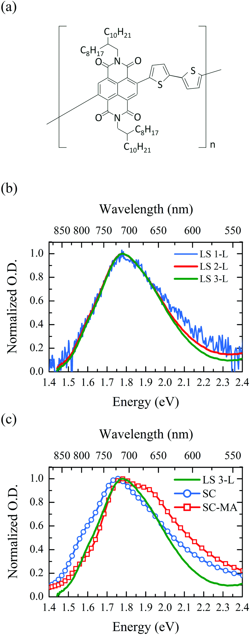 | ||
| Fig. 1 (a) P(NDI2OD-T2) molecular structure; (b) normalized UV-Vis optical absorption of LS deposited 1, 2 and 3 layers of P(NDI2OD-T2) samples; (c) normalized UV-Vis optical absorption of LS deposited three layers (LS 3-L) together with a spin-coated thin film of P(NDI2OD-T2) before (SC) and after (SC-MA) a melting treatment. | ||
In order to clarify the interplay of the different layers in defining the opto-electronic and transport properties of the films, we have adopted optical (UV-Vis absorption spectroscopy) and electrical (current–voltage characteristics of FET) measurements on one (1-L), two (2-L) and three (3-L) layers of P(NDI2OD-T2) deposited via the LS technique, in comparison with spin-coated films. Subsequently, Charge Modulation Spectroscopy (CMS) is employed to reveal charge-induced features in FETs where 1-L, 2-L and 3-L constitute the device active phase.35–37 Overall, we provide direct experimental evidence of the electronic independence of subsequently deposited LS monolayers, up to three layers, of the invariance of their opto-electronic and transport properties and the consequent 2D nature of the charge accumulated channel. In addition to the experimental evidence, we corroborate the occurrence of true 2D charge transport in molecularly ordered OFETs from a numerical point of view by means of kinetic Monte Carlo (MC) simulations.
Results and discussion
UV-Vis absorption
LS mono-layers were obtained by spreading a 0.1 mg ml−1 solution of P(NDI2OD-T2) on water, followed by the application of a compressing force that induces compact packing of the molecules at the air/liquid interface. The deposition was then carried out at a surface pressure of about 25 mN m−1, by approaching hexamethyldisilazane (HMDS)-treated glass substrates horizontal to the air/water interface. This surface pressure allows for the self-assembly of well-ordered films with a preferential edge-on molecular orientation with respect to the substrate over a large area.19 Surface pressure versus mean monomeric area isotherm curves (ESI,† Fig. S1) agree with the area per repeat unit (∼55 Å2) calculated for a P(DNI2OD-T2) Langmuir close-packed monolayer having an out-of-plane molecular order (more details in the ESI†). While it was possible to record the absorption spectra of 2-L and 3-L samples with a standard spectrophotometer, for the measurement of the 1-L sample we resorted to a lock-in detection technique, because of the very low optical density (OD). Moving the sample periodically in and out of the probing light beam, we managed to produce a transmitted light signal T modulated at a fixed and known frequency. This signal is then selectively detected with a lock-in amplifier granting the possibility to detect a reduction in transmittance ΔT, with respect to the glass substrate reference, as low as 10−5–10−6, eventually allowing the measurement of an optical density of the order of 10−3 (details can be found in the Methods section). A comparison of the three spectra (Fig. 1b) normalized at the absorption peak shows that, apart from a slight deviation at high energies, between 1.4 and 2.3 eV all samples have basically the same absorption spectrum. Irrespective of the number of layers deposited, the spectrum is characterized by a broad absorption consisting of three overlapping spectral features with a main optical transition peaked at ∼1.8 eV. The optical density (OD) of different samples (Fig. S2, ESI†) increases with the number of LS layers from OD ≈ 0.003 for 1-L to OD ≈ 0.007 for 3-L at the absorption peak. Bearing in mind that 2-L and 3-L are obtained as a stack of subsequently deposited single layers, the absence of any spectral shape evolution going from 1-L to 3-L indicates that from an optical point of view each successive layer is identical to the previous one and unaffected by the presence of others.When compared to the optical absorption spectrum of a spin-coated (SC) reference thin film processed from dichlorobenzene, a typical solvent adopted to deposit P(NDI2OD-T2), LS-deposited samples display a slight blue-shift of the main peak, along with a partial quenching of the spectral feature at 1.55 eV (Fig. 1c). Both the aforementioned spectral differences between the LS and SC samples are also observed when the SC sample is compared with a P(NDI2OD-T2) thin film treated with a melt-annealing procedure (SC-MA),31,38 also reported for comparison in Fig. 1c (details of the thermal treatment are reported in the Methods section). It is worth noticing that on the one hand with respect to the SC-MA sample, the quenching of the shoulder at 1.55 eV is only partial, while on the other hand no significant growth of the transition at 1.90 eV is observable. The spectral feature at 1.55 eV has been previously ascribed to a well-defined aggregate-induced inter-molecular transition,39 while, according to previously published DFT calculations, the feature at 1.90 eV, stemming from the linear combination of the excited states of two interacting chromophores, is expected to preserve the properties of a single chain transition.38 Both of them are particularly sensitive to the packing motif of the molecules and while the first transition is quenched upon thermal treatment, the latter is enhanced. Thus, the reported observations suggest that the LS deposition leads to a reduced aggregate content, while retaining a molecular packing motif typical of the SC thin film.
Electrical characterization
We have then evaluated the charge transport properties of 1-L, 2-L and 3-L samples in top-gate, bottom-contact FETs, depositing the three films on HMDS-treated glass substrates with photolithographically pre-patterned thin (15 nm) gold electrodes. As a dielectric we used a low-k (k = 2.1) perfluorinated 550 nm thick CYTOP layer (Fig. 2a). Remarkably, the n-channel saturation (drain–source voltage, VDS = 60 V) transfer characteristic curves of all devices (Fig. 2b) are almost identical, with a very minor difference in currents (∼15% of the 3-L current) at high gate–source voltage (VGS) and a limited difference in the subthreshold regime at low VGS. Correspondingly, for all devices we extracted identical saturation mobility values (μsat) of 0.022 ± 0.002 cm2 V−1 s−1 at sufficiently high VGS. Therefore, also from an electrical point of view, we do not see any evolution in charge transport properties with the addition of layers. Different from previous reports on ultrathin polymer films, where currents and mobility saturation were obtained after a few molecular layers,19–21 here we achieve saturation already at a layer thickness of one molecular strand. Since no advantage is gained with additional molecular layers, and since the mobility in 1-L is already higher than the plateau value of 0.018 cm2 V−1 s−1 previously reported for 6 or more P(NDI2OD-T2) LS layers over 50 μm long channels,19 we safely conclude that a single layer is not limiting the charge transport and that efficient percolation pathways are present already within a monolayer. It is worth noting that always the last deposited layer is involved in transport, since it is the one coming into contact with the gate dielectric and it will therefore be the one hosting the accumulation layer.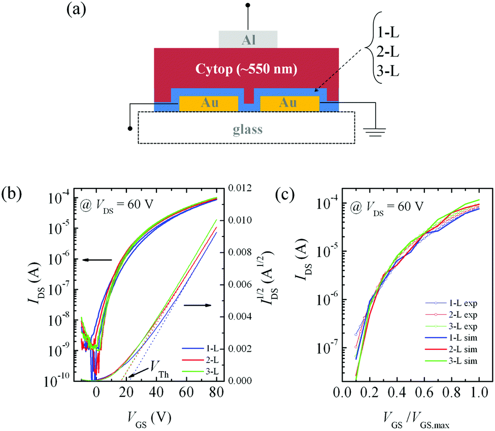 | ||
| Fig. 2 (a) Sketch of FET architecture employed in this work; (b) experimental transfer characteristic curves of 1-L (blue line), 2-L (red line) and 3-L (green line) based OFETs; (c) simulated transfer characteristic curves of 1-L (blue line), 2-L (red line) and 3-L (green line) based OFETs; for comparison, experimental curves are also reported in this panel (open circles). | ||
Lower mobility values for 1-L, 2-L and 3-L were reported in past reports on the LS transferred P(NDI2OD-T2) film19,30 where an eventual inherent dependence of channel integrity and coverage on film thickness was still plausible. By optimizing the deposition method, we now obtain a polymer monolayer with identical transport properties of a multilayer, so that any dependence of transport properties on film thickness can be definitely excluded, in much better agreement with the measurement of invariant thermal activation energy reported by Fabiano et al.30
We also highlight that with a single molecular strand, like in the 1-L case, common advantages of top-gate architecture with respect to a bottom gate are evidently not valid anymore, especially in terms of more ideal energetics at the semiconductor–polymer dielectric interface.40 The latter may only explain the small differences between 1-L and the other films in the subthreshold behavior, a bias range more sensitive to the presence of trap states and/or wider density of states. However, the identical mobilities at high VGS, i.e. in full accumulation, of 1-L, 2-L and 3-L samples contrast with the consolidated idea that a more efficient transport occurs at the interface with polymer dielectrics. Albeit functionalized with HMDS, the interface with glass should be less ideal for transport, especially in the case of n-type materials.41 Irrespective of this, the two interfaces with glass and polymer dielectric are physically very different, and it is rather remarkable not to observe any difference when the channel is accumulated in the top layer of 2-L and 3-L samples. Thus this represents a direct observation of the effective electronic isolation of the first monolayer from strong substrate-induced detrimental effects on transport. There has not been a similar observation for polymer ultra-thin films so far.19–21 We can rationalize this finding as an effect of the aliphatic solubilizing side chains that, because of the specific edge-on configuration, acts as a spacer in between the conjugated backbone and the dielectric.26 Indirectly we also have a confirmation that the nanostructure of each layer is defined at the water–air interface during the LS procedure, and that there is no influence of the underlying layers or substrate on the film morphology and electronic properties upon subsequent transfer of each monolayer.
Monte Carlo (MC) simulations
To further strengthen the evidence of 2D transport as inferred by UV-Vis absorption spectroscopy and electrical characterization, we investigated charge transport by means of kinetic Monte Carlo (MC) simulations. MC simulations represent a simplified real-world experiment with the ability to control all aspects of sample and measurement. The model of the LS layered OFETs consists of a stack of a gate dielectric and a number of semiconductor monolayers in the z-direction, where the material parameters have been chosen to represent the P(NDI2OD-T2) OFETs used in this work. Transport of Coulombically interacting charges in the semiconductor layer is assumed to occur via nearest neighbor hopping with Miller–Abrahams rates on a rectangular lattice between localized sites distributed in energy according to an exponential distribution. The gate field is applied along the z-axis and a source–drain field along the y-axis directs the movement of the charges in the system. The magnitude of the said field has been chosen to be at least one order of magnitude lower than the gate field. Further technical details concerning the MC algorithm can be found in ref. 42 and 43.The obtained transfer characteristics are shown in Fig. 2c, along with a direct comparison with experiments. An energetic disorder of 80 meV was required to consistently fit the data. The layer height and lateral lattice spacing were set to 3 nm and 1 nm, respectively, obtaining a rectangular unit cell, which better mimics the unit cell of the actual material where each edge-on LS strand is ∼3 nm thick.19 The magnitude of the current has been scaled to fit the experimental values of the 1-L device at the highest gate field. As it can be seen, the gate field dependence is well reproduced in the simulations, and the simulated current is only mildly modulated by the number of layers, with the total variation just slightly higher than in the experimental curves (∼35% of the 3-L current). The absence of a marked thickness dependence is in contrast to the work by Sharma et al.,24 where additional layers were found to affect the current. We attribute this difference to the rectangular unit cell of the present system, 3 × 1 × 1 nm3vs. 1 × 1 × 1 nm3 used in ref. 24, which is chosen because of the particular LS layer morphology. From a numerical point of view, such a unit cell enhances the confinement by the gate field and reduces the tunneling rates between successive monolayers, both enhancing the 2D nature of the charge transport. The slight dependence on the number of layers at lower gate fields, which is also observed in experiments, stems from the consideration that the carriers are distributed over multiple monolayers (if present) before being confined to the first monolayer at stronger gate fields, as discussed below in more detail.
It is noteworthy that, in the simulation, the gate field dependence of the current is strongly dependent on the energetic disorder of the semiconductor where a strong and weak energetic disorder leads to a strong and weak field dependence of the current, respectively. This allows for a relatively precise estimate of the actual (exponential) disorder of 80 ± 10 meV.
Charge modulation spectroscopy investigation
We have further investigated the transport properties of mono- and multi-layer FETs by adopting charge modulation spectroscopy (CMS) as a direct probe of the charge-induced spectral features in the different samples.44 CMS measures the spectral transmission variation (ΔT), normalized to total transmission (ΔT/T), induced by a modulation of the charge density in the channel obtained through the modulation of the FET gate voltage. This technique is inherently sensitive only to conjugated segments visited by the charge within the molecular films. Since the charge-induced ΔT is usually a very low signal, a lock-in detection system is typically adopted: the gate voltage is modulated at a certain frequency while a light beam is focused on the sample, generating a ΔT signal at the same frequency, which is then collected through a lock-in amplifier. This signal is then normalized to the transmittance value in the absence of any accumulated charge and plotted as a function of the impinging photon energy.The CMS spectra collected on the 1-L, 2-L and 3-L FETs (Fig. 3a) are identical; very small deviations are within the experimental error. The positive band (ΔT > 0), corresponding to the bleaching signal due to the reduced ground-state absorption, confirms the same shape of the optical absorption spectrum for all samples irrespective of the number of layers (Fig. 1b). The negative charge-induced absorption (ΔT < 0), peaked at 1.45 eV, proves that charge carrier relaxation and the energetic landscape probed by the charge carriers are not changing upon increasing the number of layers. In between the two main features, from 1.60 to 1.65 eV, the region with ΔT ≈ 0 is a result of the compensation between an absorption and a bleaching feature.38 Compared to the CMS spectrum of an SC film, where the two features at 1.55 eV and at 1.65 eV (previously discussed in ref. 38) can be distinguished, the spectra of the LS layers flatten because of the partial suppression of the 1.55 eV transition in the ground-state absorption (Fig. 3a). CMS measurements therefore indicate that all LS layers are structurally and energetically identical and that they are very weakly coupled.
 | ||
| Fig. 3 (a) Charge Modulation Spectra (CMS) collected from OFETs based on 1, 2 and 3 LS deposited semiconducting layers. (b) Numerically determined percentage of the total number of charge carriers in the first monolayer as a function of gate field for OFETs of different thickness as indicated by the legend. The data set is the same as used in Fig. 2b. (c) Sketch representing the confinement of the charge within the first polymer monolayer at the dielectric/semiconductor interface in full accumulation. | ||
We verified such interpretation of the experimental data by further MC simulations. The time-dependent nature of the MC algorithm allows us to track the position of every carrier at every point in time, which gives a unique and unambiguous opportunity to investigate the dimensionality of the charge transport. As a measure of this, the percentage of charge carriers in the first monolayer is plotted as a function of gate field for 1-L, 2-L and 3-L based FETs in Fig. 3b. The data set rationalizes Fig. 3a by showing that at larger gate fields the vast majority of all charges sits in the first monolayer in contact with the dielectric, irrespective of the total number of layers; at low gate fields lower lying layers do get populated, which leads to the observed minor thickness-dependence of the current. The various factors contributing to this dependence are beyond the scope of the present work and are extensively discussed in ref. 24.
It is also worth noting that there is a qualitative agreement between this work and the work by Maddalena et al.45 where, for a thin-film of P(NDI2OD-T2) deposited by spin-coating, an accumulation channel depth of ∼2 nm at high gate voltage was estimated.
The direct evidence provided by CMS investigations, along with the MC simulations, further strengthens the I–V data previously reported and proves the 2D nature of charge distribution in LS devices, where percolation pathways are efficiently established within electronically independent molecular monolayers (see the sketch in Fig. 3c). The same aliphatic chains which hinder the effect of the dielectric interface introduce a transversal energetic barrier in between molecular layers, the height of which can reach hundreds of meV,30,46 and are responsible for the electronic independence of the subsequent layers.
Thermal annealing effects
To assess whether the observed thickness independence originates from the specific layer-by-layer deposition method adopted, or a more general feature for P(NDI2OD-T2), we have investigated the transport properties and CMS features of 1-L, 2-L and 3-L films after a thermal treatment on films above the melting temperature. Melt-annealing at 350 °C and slow-cooling at a rate of 10 °C min−1 were employed to provide sufficient thermal energy and time for the backbones and side-chains to rearrange and relax into an energetic minimum which can largely differ from the one imposed by LS procedure. The same conditions have been extensively employed in the literature on P(NDI2OD-T2) samples, producing edge-on films with improved crystallinity and reduced intra-crystallite disorder starting from spin-coated films.32,47–49 In this way we obtained three films, namely 1-L MA, 2-L MA and 3-L MA, with molecular content identical to 1-L, 2-L and 3-L, respectively, and a microstructure defined by the cooling process. FET devices based on 1-L MA, 2-L MA and 3-L MA are characterized by a large threshold voltage (VT) shift, similar to what was reported in the case of melt-annealing of spin-coated samples (Fig. 4a). Such a shift is largely ascribable to an increased contact resistance in the OFETs after annealing.38 In MA films we measure a clear dependence of the device currents with the number of layers, with a fivefold increase passing from 1 to 3 layers. When we extract the field-effect mobility at the same VG − VT value, we correspondingly record an increase of mobility with increasing thickness, from 0.01 cm2 V−1 s−1 to 0.04 cm2 V−1 s−1 and 0.07 cm2 V−1 s−1 for 1-L MA, 2-L MA and 3-L MA samples, respectively. This largely deviates from what was observed in the LS films indicating that when molecules can reassemble, the film properties do change substantially. | ||
| Fig. 4 (a) Transfer characteristic curves of melt-annealed 1-L (blue line), 2-L (red line) and 3-L (green line) based OFETs. (b) Charge Modulation Spectra (CMS) collected from OFETs based on 1, 2 and 3 LS deposited semiconducting layers of P(NDI2OD-T2) after the melting procedure and (c) from the melt annealed spin coated (SC MA) sample. | ||
We have also recorded the CMS spectra for MA samples (Fig. 4b). The changes in the spectra observed with respect to LS films are similar to what was previously observed by melt-annealing pristine, spin-coated films.38 The charge-induced absorption is fairly identical in all MA samples: here the 1.65 eV feature becomes much more prominent with respect to LS films due to a complete suppression of the excitonic ground-state absorption at 1.55 eV. MA spectra instead show differences in the bleaching signal as a function of the number of layers, with a progressive increase of the band around ∼1.9 eV. Such evolution, not present in the pristine LS films, brings the spectrum of the 3-L MA sample to be very close to the spectrum measured in a MA spin-coated film (Fig. 4c). We also note that the 3-L MA film reaches a mobility value approaching that of bulkier SC film after undergoing the same treatment (μsat = 0.1 cm2 V−1 s−1).38 Both charge transport and CMS measurements indicate that the LS structure is lost and the film has re-arranged similar to what occurs in spin-coated thin films upon the same melting treatment. Importantly, the dependence on the number of ML indicates that the strict 2D nature of the pristine LS-films is lost upon melt annealing. Thus the film thickness independence observed in LS films is due to the successive deposition of complete monolayers whose microstructure is pre-formed at the air–water interface.
In contrast to the experimental findings, no ML dependence is observed for simulations performed on rectangular lattices (see also Fig. S5, ESI†). Simulations on a cubic lattice, however, were previously found to result in a ML dependence.24 As explained above, the 2D confinement is strongly enhanced by the rectangular unit cell. Hence, morphological irregularities introduced into the well-defined structure of the LS films by melt annealing will give rise to sites with a distribution of shorter inter-monolayer distances which reduces the penalty for hopping away from the first monolayer and allows percolation pathways to extend further into the material, i.e. in between what used to be individual layers. At the same time (a distribution of) larger in-plane hopping distances will be formed, further enhancing the tendency for out-of-plane hopping. The thickness dependence of melt-annealed devices might therefore be attributable to a less perfect packing of the layers. Unfortunately, a continuous distribution of inter-site distances cannot be accounted for in our MC model.
Experimental methods
OFET fabrication and electrical characterization
Thoroughly cleaned 1737F glass or SiO2 was used as a substrate for all the films realized in this work. FETs were fabricated according to a Top-Gate, Bottom-Contact architecture. Bottom Au contacts were defined by a lift-off photolithographic process with a 1.5 nm thick Cr adhesion layer. The thickness of the Au contacts was 15 nm. Patterned substrates were cleaned in an ultrasonic bath in isopropyl alcohol for 2–3 min before deposition of the semiconductor. The 1-L, 2-L and 3-L P(NDI2OD-T2) films were transferred on the substrate using the Langmuir–Schäfer (LS) technique as described above. As the dielectric layer, the perfluorinated polymer CYTOP CTL-809 M dielectric (Asahi Glass) was spun as received at 6000 rpm for 90 s (film thickness ∼550 nm); thermally evaporated 4.5 nm thick Au transparent gate electrodes were employed. The electrical characteristics of transistors were measured in a nitrogen glovebox on a Wentworth Laboratories probe station with an Agilent B1500A semiconductor device analyzer. Saturation charge carrier mobility values were extracted by the transfer characteristic curves according to the gradual channel approximation, following the expression IDS = μsat × Cdie × W/2L × (VGS − VTh)2, where IDS is the drain current, μsat is the saturation mobility, Cdie is the specific dielectric capacitance, W and L are the width and the length of the channel, respectively, VGS is the gate voltage, VDS is the drain voltage, and VTh is the threshold voltage. Accordingly, μsat was obtained from the slope of IDS0.5versus VGS, calculated every three points around each VGS value.UV-Vis absorption
The absorption measurements were performed using a spectrophotometer (Perkin Elmer Lambda 1050). The sample for the absorption measurements was prepared by the LS deposition on glass substrates according to the same recipe used for OFET preparation described above in the sample preparation part. In the case of the 1-L sample, the absorption was below the spectrometer resolution. Thus, in order to improve the signal to noise ratio, we moved to a lock-in detection technique. Mounting the sample on a chopper blade rotating at a fixed frequency f and focusing a monochromated tungsten lamp on it, we managed to get a transmitted light signal modulated at a known frequency. Notice that the actual rotation frequency was determined by shining a monochromatic CW light source on the same blade and then using its transmission as a reference. We then demodulated the transmitted white signal with a DSP lock-in in order to get the 1-L sample transmittance T. Eventually the absorption was defined as 1 − T.Charge modulation spectroscopy
The CMS spectra were collected by measuring the normalized transmittance variation (ΔT/T) induced by the gate voltage modulation. We performed the measurements keeping the source and drain electrode at 0 V, while the modulated voltage (f = 983 Hz) was applied at the gate electrode. The light of a tungsten lamp was monochromated and subsequently focused on the device. The transmitted portion of the light was then detected through a silicon photodiode. The electrical signal is amplified through a trans-impedance amplifier (Femto DHPCA-100) and then revealed through a DSP lock-in amplifier (Stanford Instrument SR830). All the measurements were performed in a vacuum atmosphere (∼10−5–10−6 mbar).Kinetic Monte-Carlo simulations
The MC experiments were performed with the temperature set to T = 300 K in a box containing 70 × 70 × N lattice sites in the x-, y- and z-direction, respectively, where N is the number of monolayers. As described above, the inter-site distance was chosen to be 1 × 1 × 3 nm3 for rectangular lattices and 1 × 1 × 1 nm3 for cubic lattices, where the hopping probabilities scale with distance as pd ∝ e−2α(ad−a0), where α = 2 × 10⁹ m−1 is the inverse localization length, ad is the lattice constant in the direction of the hop and a0 is a reference lattice constant. The number of particles in the box is set by Vg and the areal capacitance of the gate, and was between several tens and several hundreds for the field range considered in this work. Every current data point is the result of averaging over 20 configurations, where the convergence of every simulation was ensured. Interactions of twin charges resulting from the periodic boundary conditions in the x- and y-direction have been included for all carriers up to 5 box sizes away, at which point these interactions become negligible. Image charges of all charges and their twins in the z-direction arise due to the difference in the dielectric constant between the semiconductor ε1 = 3.6 and the substrate ε2 = 4.7 (the gate dielectric was set to have the same dielectric constant as the semiconductor). The electric potential in the semiconductor due to self-interaction of charge q was calculated according to ref. 24 as where ε0 is the vacuum permittivity, r is the distance between the charge and its image in the substrate in the z-direction and
  is the total charge induced by charge q in the substrate.
Conclusions
For the first time for a solution processed polymer semiconductor, we have observed the saturation of FET device currents and mobility already with a single molecular layer, and a consequent independence of FET performances from the number of monolayers. Overall our FETs' electrical and CMS data allow us to identify a scenario in which, within each single monolayer, energetically identical charge carrier states are equally sustained in a strictly 2D percolation path. The 2D transport derives from an interlayer hopping penalty reflecting a specific microstructure obtained by the LS technique where monolayers, pre-formed at the air–water interface and unmodified upon transfer to substrates, share the short- and long-range morphology. Interestingly, charge transport in such molecular layers is not affected by the usual defectivity associated with glass substrates treated with short hydrophobic molecules, likely favored by the high compactness of the LS molecular strand which packs with an edge-on motif. When melting and slow cooling processes are adopted, allowing the LS layers to reassemble and interact, the LS-induced microstructure, and therefore the strict 2D nature of both optical and electronic properties, is lost, and the thickness dependence is reintroduced. This confirms the paramount importance of the supra-molecular self-organization in the determination of polymer semiconductor charge transport properties.Acknowledgements
This work has been in part financially supported by the European Research Council (ERC) under the European Union's Horizon 2020 research and innovation programme ‘HEROIC’, grant agreement 638059. H. A. gratefully acknowledges funding from the Knut och Alice Wallenbergs stiftelse (project ‘Tail of the Sun’). S. F. acknowledges support from the Advanced Functional Materials Center at Linköping University (No. 2009-00971) and VINNOVA (No. 2015-04859).Notes and references
- M. Caironi and Y. Y. Noh, Large Area and Flexible Electronics, Wiley-VCH Verlag GmbH & Co. KGaA, 2015 Search PubMed.
- H. Sirringhaus, Adv. Mater., 2014, 26(9), 1319–1335 CrossRef CAS PubMed.
- A. C. Arias, J. D. MacKenzie, I. McCulloch, J. Rivnay and A. Salleo, Chem. Rev., 2010, 110(1), 3–24 CrossRef CAS PubMed.
- R. P. Fornari and A. Troisi, Adv. Mater., 2014, 26(45), 7627–7631 CrossRef CAS PubMed.
- D. Gargi, R. J. Kline, D. M. DeLongchamp, D. A. Fischer, M. F. Toney and B. T. O'Connor, J. Phys. Chem. C, 2013, 117, 17421–17428 CAS.
- R. Noriega, J. Rivnay, K. Vandewal, F. P. V. Koch, N. Stingelin, P. Smith, M. F. Toney and A. Salleo, Nat. Mater., 2013, 12, 1038 CrossRef CAS PubMed.
- D. Venkateshvaran, M. Nikolka, A. Sadhanala, V. Lemaur, M. Zelazny, M. Kepa, M. Hurhangee, A. J. Kronemeijer, V. Pecunia, I. Nasrallah, I. Romanov, K. Broch, I. McCulloch, D. Emin, Y. Olivier, J. Cornil, D. Beljonne and H. Sirringhaus, Nature, 2014, 515(7527), 384–388 CrossRef CAS PubMed.
- D. Fazzi and M. Caironi, Phys. Chem. Chem. Phys., 2015, 17(14), 8573–8590 RSC.
- S. Wang, S. Fabiano, S. Himmelberger, S. Puzinas, X. Crispin, A. Salleo and M. Berggren, Proc. Natl. Acad. Sci. U. S. A., 2015, 112(34), 10599–10604 CrossRef CAS PubMed.
- I. V. Klimovich, L. I. Leshanskaya, S. I. Troyanov, D. V. Anokhin, D. V. Novikov, A. A. Piryazev, D. A. Ivanov, N. N. Dremova and P. A. Troshin, J. Mater. Chem. C, 2015, 2(36), 7621–7631 RSC.
- E. L. Granstrom and C. D. Frisbie, J. Phys. Chem. B, 1999, 103(42), 8842–8849 CrossRef CAS.
- F. Dinelli, M. Murgia, P. Levy, M. Cavallini, F. Biscarini and D. M. de Leeuw, Phys. Rev. Lett., 2004, 92(11), 116802 CrossRef PubMed.
- R. Ruiz, A. Papadimitratos, A. C. Mayer and G. G. Malliaras, Adv. Mater., 2005, 17(14), 1795–1798 CrossRef CAS.
- A. Shehu, S. D. Quiroga, P. D'Angelo, C. Albonetti, F. Borgatti, M. Murgia, A. Scorzoni, P. Stoliar and F. Biscarini, Phys. Rev. Lett., 2010, 104(24), 246602 CrossRef PubMed.
- M. Kiguchi, M. Nakayama, T. Shimada and K. Saiki, Phys. Rev. B: Condens. Matter Mater. Phys., 2005, 71(3), 035332 CrossRef.
- T. Muck, V. Wagner, U. Bass, M. Leufgen, J. Geurts and L. W. Molenkamp, Synth. Met., 2004, 146(3), 317–320 CrossRef CAS.
- F. Zhang, C.-A. Di, N. Berdunov, Y. Hu, Y. Hu, X. Gao, Q. Meng, H. Sirringhaus and D. Zhu, Adv. Mater., 2013, 25(10), 1401–1407 CrossRef CAS PubMed.
- L. Jiang, H. Dong, Q. Meng, H. Li, M. He, Z. Wei, Y. He and W. Hu, Adv. Mater., 2011, 23(18), 2059–2063 CrossRef CAS PubMed.
- S. Fabiano, C. Musumeci, Z. Chen, A. Scandurra, H. Wang, Y. L. Loo, A. Facchetti and B. Pignataro, Adv. Mater., 2012, 24(7), 951–956 CrossRef CAS PubMed.
- S. Wang, W. Pisula and K. Müllen, J. Mater. Chem., 2012, 22(47), 24827 RSC.
- B. M. I. Flier, M. C. Baier, J. Huber, K. Müllen, S. Mecking, A. Zumbusch and D. Wöll, J. Am. Chem. Soc., 2012, 134(1), 480–488 CrossRef CAS PubMed.
- A. J. Kronemeijer, V. Pecunia, D. Venkateshvaran, M. Nikolka, A. Sadhanala, J. Moriarty, M. Szumilo and H. Sirringhaus, Adv. Mater., 2014, 26(5), 728–733 CrossRef CAS PubMed.
- J. J. Brondijk, W. S. C. Roelofs, S. G. J. Mathijssen, A. Shehu, T. Cramer, F. Biscarini, P. W. M. Blom and D. M. de Leeuw, Phys. Rev. Lett., 2012, 109(5), 056601 CrossRef CAS PubMed.
- A. Sharma, F. W. A. van Oost, M. Kemerink and P. A. Bobbert, Phys. Rev. B: Condens. Matter Mater. Phys., 2012, 85(23), 235302 CrossRef.
- L. Demeyu, S. Stafström and M. Bekele, Phys. Rev. B: Condens. Matter Mater. Phys., 2007, 76(15), 155202 CrossRef.
- H. Yan, Z. Chen, Y. Zheng, C. Newman, J. R. Quinn, F. Dotz, M. Kastler and A. Facchetti, Nature, 2009, 457(7230), 679–686 CrossRef CAS PubMed.
- Z. Chen, Y. Zheng, H. Yan and A. Facchetti, J. Am. Chem. Soc., 2008, 131(1), 8–9 CrossRef PubMed.
- M. Gleiche, L. F. Chi and H. Fuchs, Nature, 2000, 403(6766), 173–175 CrossRef CAS PubMed.
- B. Pignataro, J. Mater. Chem., 2009, 19(21), 3338–3350 RSC.
- S. Fabiano, H. Yoshida, Z. Chen, A. Facchetti and M. A. Loi, ACS Appl. Mater. Interfaces, 2013, 5, 4417–4422 CAS.
- T. Schuettfort, S. Huettner, S. Lilliu, J. E. Macdonald, L. Thomsen and C. R. McNeill, Macromolecules, 2011, 44(6), 1530–1539 CrossRef CAS.
- T. Schuettfort, L. Thomsen and C. R. McNeill, J. Am. Chem. Soc., 2013, 135(3), 1092–1101 CrossRef CAS PubMed.
- W. Porzio, G. Scavia, L. Barba, G. Arrighetti and C. R. McNeill, Eur. Polym. J., 2014, 61, 172–185 CrossRef CAS.
- S. G. Bucella, A. Luzio, E. Gann, L. Thomsen, C. R. McNeill, G. Pace, A. Perinot, Z. Chen, A. Facchetti and M. Caironi, Nat. Commun., 2015, 6, 8394 CrossRef CAS PubMed.
- M. Caironi, M. Bird, D. Fazzi, Z. Chen, R. Di Pietro, C. Newman, A. Facchetti and H. Sirringhaus, Adv. Funct. Mater., 2011, 21, 3371 CrossRef CAS.
- A. Luzio, L. Criante, V. D'Innocenzo and M. Caironi, Sci. Rep., 2013, 3, 3425 Search PubMed.
- N. Martino, D. Fazzi, C. Sciascia, A. Luzio, M. R. Antognazza and M. Caironi, ACS Nano, 2014, 8(6), 5968–5978 CrossRef CAS PubMed.
- V. D'Innocenzo, A. Luzio, A. Petrozza, D. Fazzi and M. Caironi, Adv. Funct. Mater., 2014, 24(35), 5584–5593 CrossRef.
- R. Steyrleuthner, M. Schubert, I. Howard, B. Klaumünzer, K. Schilling, Z. Chen, P. Saalfrank, F. Laquai, A. Facchetti and D. Neher, J. Am. Chem. Soc., 2012, 134(44), 18303–18317 CrossRef CAS PubMed.
- H. Sirringhaus, Adv. Mater., 2005, 17(20), 2411–2425 CrossRef CAS.
- H. Phan, M. Wang, G. C. Bazan and T.-Q. Nguyen, Adv. Mater., 2015, 27(43), 7004–7009 CrossRef CAS PubMed.
- A. Melianas, V. Pranculis, A. Devižis, V. Gulbinas, O. Inganäs and M. Kemerink, Adv. Funct. Mater., 2014, 24(28), 4507–4514 CrossRef CAS.
- A. Melianas, F. Etzold, T. J. Savenije, F. Laquai, O. Inganäs and M. Kemerink, Nat. Commun., 2015, 24, 4507–4514 CrossRef.
- P. J. Brown, H. Sirringhaus, M. Harrison, M. Shkunov and R. H. Friend, Phys. Rev. B: Condens. Matter Mater. Phys., 2001, 63(12), 125204 CrossRef.
- F. Maddalena, C. de Falco, M. Caironi and D. Natali, Org. Electron., 2015, 17, 304–318 CrossRef CAS.
- J. C. Blakesley, M. Schubert, R. Steyrleuthner, Z. Chen, A. Facchetti and D. Neher, Appl. Phys. Lett., 2011, 99(18), 183310 CrossRef.
- J. Rivnay, R. Steyrleuthner, L. H. Jimison, A. Casadei, Z. Chen, M. F. Toney, A. Facchetti, D. Neher and A. Salleo, Macromolecules, 2011, 44(13), 5246–5255 CrossRef CAS.
- J. Rivnay, M. F. Toney, Y. Zheng, I. V. Kauvar, Z. Chen, V. Wagner, A. Facchetti and A. Salleo, Adv. Mater., 2010, 22(39), 4359–4363 CrossRef CAS PubMed.
- M. Brinkmann, E. Gonthier, S. Bogen, K. Tremel, S. Ludwigs, M. Hufnagel and M. Sommer, ACS Nano, 2012, 6(11), 10319–10326 CrossRef CAS PubMed.
Footnote |
| † Electronic supplementary information (ESI) available: The mobility data table, additional CMS spectra, and Monte Carlo simulations for MA films. See DOI: 10.1039/c6tc03897b |
| This journal is © The Royal Society of Chemistry 2016 |