DOI:
10.1039/C6TC03818B
(Paper)
J. Mater. Chem. C, 2016,
4, 10329-10338
Lu2CaMg2(Si1−xGex)3O12:Ce3+ solid-solution phosphors: bandgap engineering for blue-light activated afterglow applicable to AC-LED†
Received
3rd September 2016
, Accepted 16th October 2016
First published on 17th October 2016
Abstract
Persistent luminescence (PersL) has long commanded the curiosity of researchers owing to the complicated and profound physics behind it. In this work, the PersL mechanism in a new kind of persistent garnet phosphors, Lu2CaMg2(Si1−xGex)3O12:Ce3+, is studied from the new perspective of a “solid-solution” scheme. Different from the conventional study in pursuit of long PersL, we focus on manipulation of afterglow to the millisecond range and tentatively demonstrate its potential to compensate the flickering of the alternating current driven LED (AC-LED) in every AC cycle. Evidently, the tailored host bandgap favors efficient electron charging and facilitates electron detrapping, as well as redeploying trap distribution, which results in a blue light activated afterglow in the millisecond time range, and subsequently a reduced percent flicker of 64.1% for the AC-LED. This investigation is the first attempt to establish the design guidelines for new PersL materials with an adjustable millisecond ranged afterglow, and, hopefully, it paves a pathway to the development of burgeoning low-flickering AC-LED technology.
1. Introduction
Bandgap engineering is an effective approach to tune the electrical and optical properties of inorganic materials through alloying or solidification of foreign elements into the host lattice to form a solid-solution.1–5 Great success has been demonstrated by adopting this design strategy to achieve efficient optoelectronic property tailoring in semiconductors, which boosts the wide application of semiconductor materials in the fields of light-emitting-diode (LED), photovoltaics, biological imaging, etc.6–9 Recently, this approach was revealed as applicable for phosphors (an insulator in nature) as well, endowing them with PersL properties,10–15 which opens up a brand-new perspective for exploring novel phosphorescent materials that are highly desirable in security signs, night displays, optical storage media, etc.16–20
PersL is an interesting phenomenon whereby luminescence from an active center still lasts for a long period after ceasing the excitation.16 However, there is some complex and profound physics behind the PersL mechanism, including excitation, delocalization, migration, storage, release, and recombination of charge carriers, which casts a veil of mystery over it. Especially, the trap properties (including the species, depth, concentration and distribution) that determine PersL behavior in a host are difficult to be identified and modulated.17,21–23 Bandgap engineering can affect not only the PersL charging process that refers to the promotion of activator electrons to the conduction band (CB) and the further storage of them in traps, but also the PersL detrapping process that relates to the liberation of immobilized electrons in traps with the aid of heat. As schematically illustrated in Fig. 1, CB lowering allows for electrons' jumping over the barrier between the excited state of rare earth ions (REI) and the CB via photoionization on one hand, and makes the trap depth closer to the CB on the other hand.10 The former effect leads to more efficient electron charging via the CB instead of quantum tunneling, while the latter might facilitate electron release from the trap at room temperature. Both of them are favorable to enhance the PersL intensity. Evidently, bandgap engineering can efficiently tailor the PersL properties, and serve as an effective tool to take a closer look at the PersL mechanism.
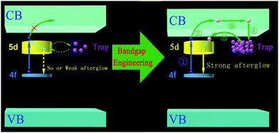 |
| | Fig. 1 Schematic illustration of the PersL mechanism including ① electron excitation, ② electron photoionization, ③ electron migration, ④ electron trapping, and ⑤ electron detrapping, and the design concept of applying bandgap engineering to achieve a more intense afterglow with a shorter duration. | |
Generally, scientists are always in pursuit of long PersL due to the strong demands of emergency lighting and identification markers. Little attention has been paid to the short afterglow, typically in the time window of milliseconds. Garlick and Wilkins first clarified that the millisecond afterglow of ZnS:Cu is dependent on the time that electrons spend in the trap.24 Kanai et al. observed the X-ray activated millisecond afterglow in a garnet crystal.25 Recently, a novel application of PersL materials in the alternating current driven LED (AC-LED) was proposed by Liu and Chen et al., since the millisecond afterglow is able to compensate the dimming time in every AC cycle.26–28 Thereafter, the blue-light activated SrSi2O2N2:Eu2+,Mn2+,26 SrAl2O4:Eu2+,Ce3+,Li+,27 SrAl2O4:Eu2+,R3+ (R = Y, Dy),28 Gd2.98Al2Ga3O12:0.02Ce3+,29 and Mg3Y2(Ge,Si)3O12:Ce3+ (ref. 30) persistent phosphors were developed for AC-LED. Despite this progress, no appropriate guidance was established for the design of blue-excited PersL materials with short afterglow in the millisecond range and, thus, more in-depth fundamental investigations are highly desired.
In this work, we exhaustively investigate the PersL behavior of Lu2CaMg2(Si1−xGex)3O12:Ce3+ (abbreviated as LCMSGO:Ce3+) solid-solution garnet phosphors, which have never been reported previously to the best of our knowledge. The bandgap engineering design concept is validated to efficiently manipulate the electron charging and detrapping for realizing blue-light excited PersL with adjustable afterglow in the millisecond range. Particularly, the trap properties are carefully examined with the aid of TL and EPR measurements. Thanks to the compensation arising from the stimulus intensity of the afterglow, flickering of the constructed AC-LED prototype device is partially compensated, demonstrating promising application of the developed LCMSGO:Ce3+ phosphors in low flickering AC-LEDs with the advantages of a cheaper price, longer lifetime, and higher energy utilization efficiency.
2. Experimental section
2.1. Preparations
Lu2CaMg2(Si1−xGex)3O12:Ce3+ (x = 0–1) samples were synthesized via a high-temperature solid-state route using high-purity chemicals (Aladin) of Lu2O3, CaO, MgO, GeO2, SiO2 and CeO2 as starting materials and a small amount of H3BO3 as flux. The CaO powder was calcined at 850 °C for 1 h before use to release the absorbed H2O and transform the possibly present CaCO3 to CaO, considering that it is very sensitive to water and carbon dioxide in the air. These compounds were weighed at the stoichiometric ratio, mixed and ground in an agate mortar for 30 min. Then, the mixture was calcined at 1300 °C for 4 hours under a 95% N2 + 5% H2 reductive atmosphere.
2.2. Characterizations
The resulting LCMSGO:Ce3+ samples were characterized using a powder diffractometer (Rigaku, Miniflex600) using Cu Kα radiation. XRD patterns were collected using the continuous scan mode with a rate of 5° min−1 for phase determination and the step scan mode with a rate of 8 s per step (step size: 0.02°) for Rietveld refinement. The microstructure observations and analyses were performed on a transmission electron microscope (TEM, JEM-2010) operating at 200 kV. The photoluminescence (PL), photoluminescence excitation (PLE), persistent luminescence (PersL), persistent luminescence excitation (PersLE) spectra, and persistent decay curves were all measured using a spectrophotometer (Edinburgh Instruments, FS920) with a 450 W xenon arc lamp as the light source. The diffuse reflection spectra of samples were measured using a UV-Vis-NIR spectrophotometer (PerkinElmer, Lambda 950), using BaSO4 as a standard reference. EPR spectra were obtained with an X-band electron paramagnetic resonance spectrometer (Bruker, ELEXSYS E500) at a frequency of 9.826 GHz before and after the samples were irradiated with 460 nm light. For the thermoluminescence (TL) measurements, the samples were mounted on a thermal stage (Linkam Scientific Instruments, THMS600E), exposed to 460 nm blue-light irradiation for 5 min at the setting temperature, and then heated to 673 K with a heating rate of 1 K s−1. Meanwhile, the luminescent intensity variation of Ce3+ by monitoring at 580 nm was recorded by employing the kinetic mode of FS920. The final TL curves were obtained by transforming the measured time dependent luminescent curves to the temperature dependent ones. The chromaticity and photometric parameters of the fabricated w-LEDs were measured in an integrating sphere of 50 cm diameter connected to a CCD detector with an optical fiber (Everfine Photo-E-Info Co. Ltd, HAAS-2000). The percent flicker of AC-LED was measured using a rapid recording photometer (Everfine Photo-E-Info Co. Ltd, Photo-2000F) with a sampling rate of 200 kS s−1.
3. Results and discussion
3.1. Micro-structure analyses
As shown in Fig. 2a, all the XRD patterns of the as-prepared LCMSGO:Ce3+ (x = 0–1) samples with various Si![[thin space (1/6-em)]](https://www.rsc.org/images/entities/char_2009.gif) :Ge molar ratios are in good agreement with that of the garnet structure. There is no appreciable signal from impurities when the Si:Ge molar ratio is lower than 2:1, while the second apatite phase (denoted by an asterisk) appears in the high-Si content sample due to destabilization of the crystal structure.31,32 With decreasing of the Si content, the XRD peaks gradually shift to the lower 2θ side. The lattice expansion induced by the replacement of Ge (r = 0.53 Å) for Si (r = 0.42 Å) should be responsible for this observation. Fig. S1a (ESI†) presents the calculated lattice constants of the samples with the aid of Jade 5.0 software, which accord well with Vegard's law, indicating the solid-solution formation. To further explore the structure variation, XRD Rietveld refinement of the Lu1.99CaMg2Si1.5Ge1.5O12:0.01Ce3+ (taken as an example) is implemented by adopting Fullprof software as the running program and crystallographic data of Y3Al3Ga2O12 (ICSD #280106) as the initial structure model (Fig. 2b). The finally obtained weighted (Rwp) and profile (Rp) R-factors are determined to be 4.98% and 3.94%, respectively, indicating that the refined atom positions, fraction factors and temperature factors of the sample satisfy the reflection conditions. The main refined structural parameters are summarized in Table 1 and Table S1 (ESI†). The high-resolution TEM (HRTEM) patterns of the LCMSGO sample and the related fast Fourier transform (FFT) image in the denoted square region are shown in Fig. 2c, indicating the single-crystalline nature. The HRTEM image shows clear lattice fringes with interplanar spacings of 0.276 and 0.248 nm, corresponding to the (240) and (422) planes of LCMSGO. The FFT image exhibits the diffraction pattern along the [2 1
:Ge molar ratios are in good agreement with that of the garnet structure. There is no appreciable signal from impurities when the Si:Ge molar ratio is lower than 2:1, while the second apatite phase (denoted by an asterisk) appears in the high-Si content sample due to destabilization of the crystal structure.31,32 With decreasing of the Si content, the XRD peaks gradually shift to the lower 2θ side. The lattice expansion induced by the replacement of Ge (r = 0.53 Å) for Si (r = 0.42 Å) should be responsible for this observation. Fig. S1a (ESI†) presents the calculated lattice constants of the samples with the aid of Jade 5.0 software, which accord well with Vegard's law, indicating the solid-solution formation. To further explore the structure variation, XRD Rietveld refinement of the Lu1.99CaMg2Si1.5Ge1.5O12:0.01Ce3+ (taken as an example) is implemented by adopting Fullprof software as the running program and crystallographic data of Y3Al3Ga2O12 (ICSD #280106) as the initial structure model (Fig. 2b). The finally obtained weighted (Rwp) and profile (Rp) R-factors are determined to be 4.98% and 3.94%, respectively, indicating that the refined atom positions, fraction factors and temperature factors of the sample satisfy the reflection conditions. The main refined structural parameters are summarized in Table 1 and Table S1 (ESI†). The high-resolution TEM (HRTEM) patterns of the LCMSGO sample and the related fast Fourier transform (FFT) image in the denoted square region are shown in Fig. 2c, indicating the single-crystalline nature. The HRTEM image shows clear lattice fringes with interplanar spacings of 0.276 and 0.248 nm, corresponding to the (240) and (422) planes of LCMSGO. The FFT image exhibits the diffraction pattern along the [2 1 ![[5 with combining macron]](https://www.rsc.org/images/entities/char_0035_0304.gif) ] zone axis.
] zone axis.
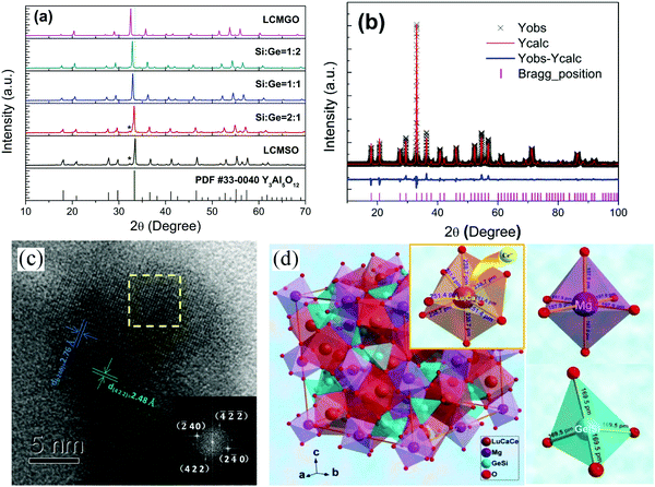 |
| | Fig. 2 (a) XRD patterns of the LCMSGO:0.01Ce3+ samples with various Si:Ge molar ratios; standard data of the Y3Al5O12 phase (PDF #33-0040) is presented as a reference. (b) Rietveld refinement of Lu1.99CaMg2Si1.5Ge1.5O12:0.01Ce3+ with the data and the fit represented by points and the line. (c) HRTEM analyses on LCMSGO and the related FFT image. (d) Crystal structure of LCMSGO, showing the dodecahedral coordination environment of Lu/Ca for Ce3+ doping, octahedral one of Mg, and tetrahedral one of Ge/Si. | |
Table 1 Crystallographic data and refinement parameters for the Lu1.99CaMg2Si1.5Ge1.5O12:0.01Ce3+ phosphor
| Atom |
Site |
x
|
y
|
z
|
Occupancy |
U (Å2) |
Space group: Ia![[3 with combining macron]](https://www.rsc.org/images/entities/char_0033_0304.gif) d(230). Symmetry: cubic. Lattice parameters: a = b = c = 12.1251 Å; V = 1782.61 Å3. Reliable factors: Rwp = 4.98%; Rp = 3.94%; χ2 = 5.86%. d(230). Symmetry: cubic. Lattice parameters: a = b = c = 12.1251 Å; V = 1782.61 Å3. Reliable factors: Rwp = 4.98%; Rp = 3.94%; χ2 = 5.86%. |
| Lu |
24c |
0.1250 |
0 |
0.2500 |
0.6633 |
0.0010 |
| Ca |
24c |
0.1250 |
0 |
0.2500 |
0.3333 |
0.0010 |
| Mg |
16a |
0 |
0 |
0 |
1.0000 |
0.0038 |
| Si |
24d |
0.3750 |
0 |
0.2500 |
0.5000 |
0.0063 |
| Ge |
24d |
0.3750 |
0 |
0.2500 |
0.5000 |
0.0063 |
| O |
96h |
0.0988 |
0.2021 |
0.2884 |
1.0000 |
0.0089 |
| Ce |
24c |
0.1250 |
0 |
0.2500 |
0.0034 |
0.0010 |
A schematic illustration of the LCMSGO crystal structure based on the refinement results is depicted in Fig. 2d. In the structure, Lu and Ca are in the dodecahedra site (24c) with four longer Lu/Ca–O bond lengths of 0.2387 nm and four shorter ones of 0.2514 nm. Mg exclusively occupies the octahedral site (16a) with Mg–O bond length of 0.1979 nm. Si and Ge locate in the tetrahedral site (24d) with Si/Ge–O bond length of 0.1695 nm. Each [(Lu/Ca)O8] dodecahedron is connected to four [MgO6] octahedrons and two [(Si/Ge)O4] tetrahedrons by sharing edges, and four [(Si/Ge)O4] tetrahedrons by sharing O2− vertexes. The activator center Ce3+ ions are expected to preferentially substitute the Lu/Ca site owing to the similar ionic radius and valence.
3.2. Electronic structure
Quantum mechanical first-principles calculations for the Ca4Lu8Si6Ge6Mg8O48 crystal were performed by the plane-wave pseudopotential method33 implemented in the CASTEP package.34 The exchange–correlation potential employed the Perdew–Burke–Ernzerhof (PBE) function35 in the framework of a generalized gradient approximation (GGA). The kinetic energy cutoffs of 500 eV and Monkhorst–Pack k-point meshes36 (2 × 2 × 2) in the Brillouin zone were chosen. The ion–electron interactions were modeled by the ultrasoft pseudopotentials37 for all elements, in which the orbital electrons Ca 3s23p64s2, Lu 4f145d15p66s2, Si 3s23p2, Ge 4s24p2, Mg 2p63s2 and O 2s22p4 were regarded as valence electrons. The bond lengths and angles were fully optimized using the BFGS method.38 All of the structure models were fully relaxed until the energy change, maximum force, maximum stress, and maximum displacement were less than 5.0 × 10⁻⁶ eV per atom, 0.01 eV Å−1, 0.02 GPa, and 5.0 × 10⁻⁴ Å, respectively. In order to solve the disordered occupation between Si/Ge and Ca/Lu atoms, the space group was changed from Iad symmetry to P1 symmetry and the atoms were set occupying every independent site alternatively according to their stoichiometric ratio (Fig. S2, ESI†). In Fig. 3a, it is clear that the top of the valence band (VB) maximum and the bottom of the CB minimum are both located at the k-point of G, demonstrating a direct bandgap with energy of ∼4.2 eV. Since the adopted GGA exchange–correlation function usually underestimates the bandgap energy, the calculated value is below the experimental one of 5.8 eV. In Fig. 3b, it is revealed that the CB bottom is determined by the 3p orbital of Si, and 4s, 4p orbitals of Ge, therefore its energy position should be greatly altered by varying the Si/Ge ratio. The VB top is mainly composed of the 4f orbital of Lu and 2p orbital of O. With increasing the Ge concentration, the bond length of Ge/Si–O is expected to be changed, which induces variations in the electron bonding energy for the O 2p orbital and then the VB top.39–41
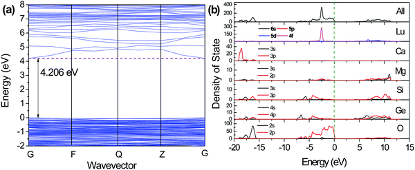 |
| | Fig. 3 (a) Calculated energy band structure of Lu2CaMg2Si1.5Ge1.5O12. (b) The total and partial (Lu, Ca, Mg, Si, Ge, O atoms) density of states for Lu2CaMg2Si1.5Ge1.5O12. | |
3.3. Luminescence and PersL property
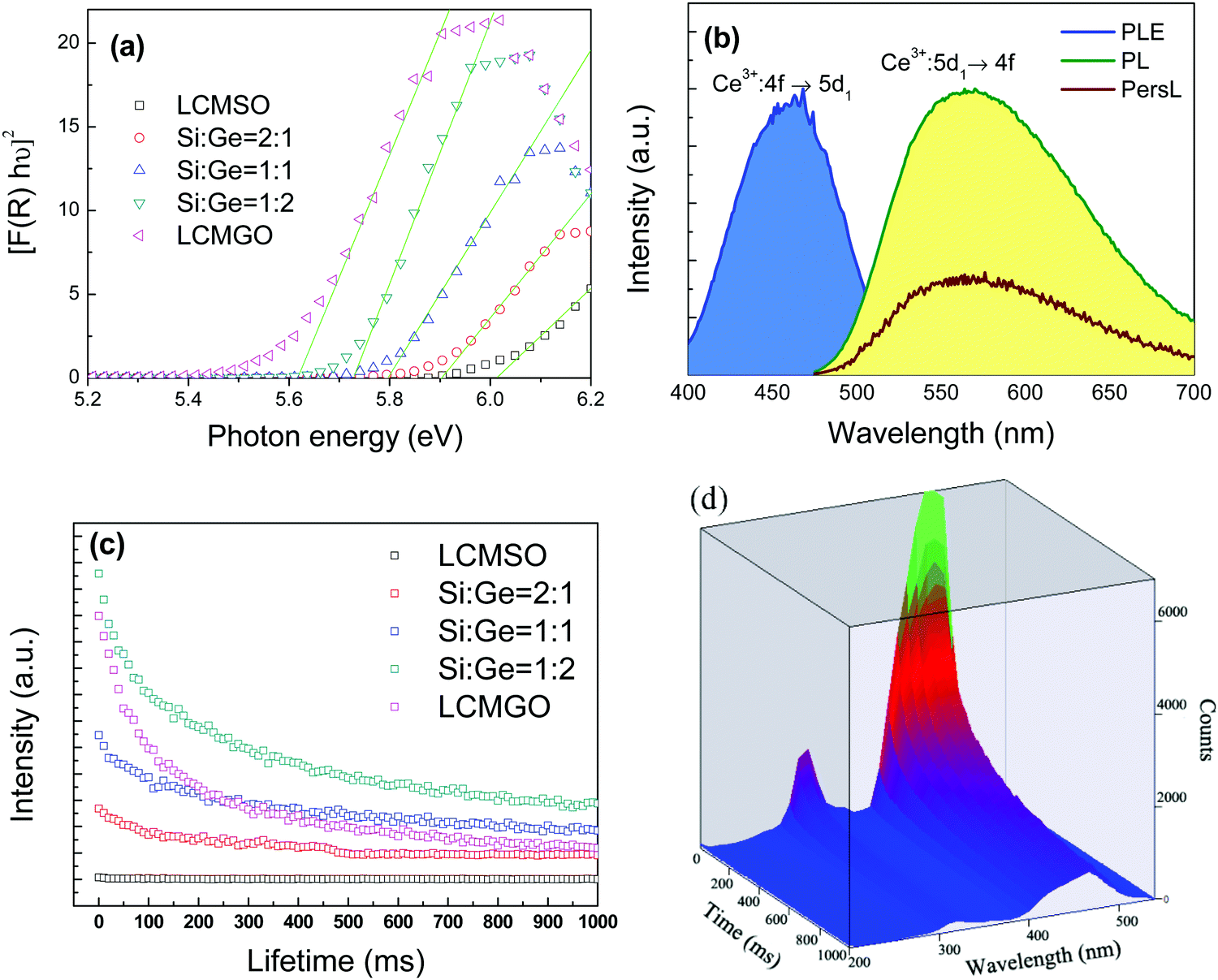
Kubelka–Munk-transformed diffuse reflectance spectra of the samples according to the formula of [F(R∞)hν]n = A(hν − Eg) are presented in Fig. 4a, where F(R∞) is the ratio of absorption coefficient to scattering coefficient, n equals 2 since the host absorption is governed by the direct allowed transitions, A is the proportional constant, hν the photon energy, and Eg the host bandgap. With variation from LCMSO to LCMGO, the calculated Eg gradually declines from 6.03 eV to 5.63 eV, obeying Vegard's law (Fig. S1b, ESI†), which confirms the successful formation of the LCMSGO solid-solution.
 |
| | Fig. 4 (a) Kubelka–Munk-transformed diffuse reflectance spectra of LCMSGO with various Si:Ge ratios; Eg is determined by extrapolating the linear portion of the Tauc plot to the photon energy axis. (b) PL, PLE, and PersL spectra of the Lu1.99CaMg2Si1.5Ge1.5O12:0.01Ce3+ sample. (c) PersL decay curves of the samples with various Si:Ge ratios. (d) PersL excitation spectra plotted by measuring the PersL decay curve at different excitation wavelengths. | |
Typical PL and PLE spectra (Fig. 4b) of the Lu1.99CaMg2Si1.5Ge1.5O12:0.01Ce3+ sample show intense Ce3+:5d1 → 4f yellow emission upon Ce3+:4f → 5d1 blue-light excitation. Owing to Lu3+/Ca2+ cation disorder in the dodecahedral site, the Ce3+ emission band is rather broad.31 It is revealed by the Si/Ge ratio dependent PL spectra in Fig. S3 (ESI†) that the emission peak wavelength shifts to the high energy side when more Ge is substituted for Si, indicating that the crystal field strength is reduced.
It is well known that there are plenty of localized imperfections in garnet phosphor sintered at high-temperature, including point defects, anti-site defects, and defect clusters, enabling garnets as potential candidates for PersL materials.10–12 LCMSGO:Ce3+ silicate garnet also contains certain defects in the crystal structure as demonstrated by the following EPR and TL tests, so bright yellow PersL can be observed after ceasing the irradiation. Fig. 4b exhibits PersL spectra of the sample, demonstrating that the PersL emissive center is originating from Ce3+. Fig. 4c shows Si/Ge ratio dependent PersL decay curves. One can see that no PersL is observed in LCMSO, while PersL emerges and becomes brighter and brighter until the Si:Ge ratio reaches 1:2; thereafter it weakens in LCMGO. The PersL lifetime, estimated by the time the luminescence decreases to 1/e of the initial intensity, is determined to be decreasing from >1000 ms, 790 ms, 410 ms to 180 ms, for Si:Ge = 2:1, 1:1, 1:2, and LCMGO samples, respectively. As known, most PersL materials developed to date should be activated at high radiation energy (e.g. ultraviolet or X-ray).16,20 Unlike that, the PersL excitation spectrum in Fig. 4d demonstrates the efficient activation of PersL in LCMSGO:Ce3+ by the blue-light irradiation. Such a unique spectral feature is the basis for AC-LED application due to the blue-emitting commercialized InGaN chip. The similar spectral profile between PLE and PersL excitation spectra suggests that efficient electron charging of PerL should proceed via the Ce3+:4f → 5d excitation. We further optimized the Ce3+ concentration and H3BO3 amount to be 2 mol% and 2 wt% to achieve the brightest PersL, as shown in Fig. S4 (ESI†).
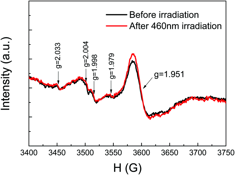
The EPR spectra of the Lu1.98CaMg2Si1.5Ge1.5O12:0.02Ce3+ sample at room temperature before and after 460 nm irradiation are shown in Fig. 5. One can see an intense EPR signal at g = 1.951 and four weaker ones at g = 1.979, 1.998, 2.004, and 2.033. These signals are attributed to the Ge-related defects featuring g values at ∼2.000, such as a Ge(1) center (an electron trapped in a tetra-coordinated Ge atom), Ge(2) center (an ionized twofold coordinated Ge obtained by releasing one electron), and an E′-Ge center (a threefold-coordinated Ge atom with an unpaired electron).42–44 Therefore, it is reasonable to postulate that the trap type in LCMSGO belongs to different kinds of Ge-related defect species, e.g., VGe–Ce3+–VO defect clusters.17,18,30 It is worth noting that there is an evident signal enhancement at g = 1.951 after irradiation. Considering the g-value of the light-enhanced EPR signal that is smaller than the g-value of a free electron (gfree−ion = 2.0023), this signal is readily assigned to the presence of trapped electrons.16,45,46
 |
| | Fig. 5 EPR spectra of the Lu1.98CaMg2Si1.5Ge1.5O12:0.02Ce3+ sample before and after 460 nm irradiation. | |
3.4. Electron charging and detrapping
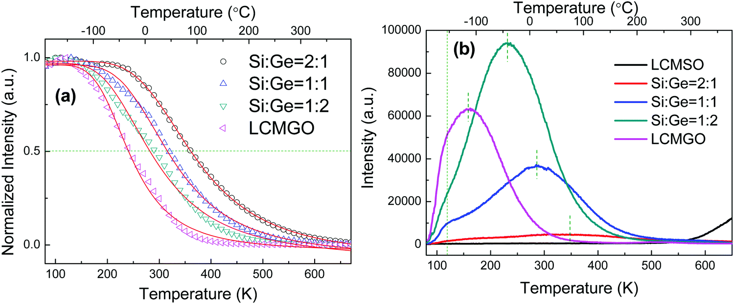
As stated above, the composition variation in the LCMSGO:Ce3+ solid-solution phosphor results in distinct PersL changes. In order to find out the inherent mechanism, electron charging and detrapping processes of PersL should be carefully examined. Fig. 6a shows the temperature dependence of the integrated PL intensity of the samples with various Si:Ge ratios (λex = 460 nm). In all the samples, one can observe temperature induced quenching. The experimental data can be well fitted by a single barrier quenching function:47| |  | (1) |
where I(T) is the luminescence intensity at temperature T, Γ0 and Γv represent the attempt rate for thermal quenching and radiative decay rate of the Ce3+:5d1 state, respectively, Eq is the energy barrier for thermal quenching, and kB is the Boltzmann constant. The estimated thermal quenching parameters are listed in Table S2 (ESI†). Obviously, both the Eq and quenching temperature (T0.5) at which the emission intensity dropped to 50% of the original level decrease with the Ge content increase. This is just as we expected, since the CB bottom lowering in the high-Ge content sample makes the thermal ionization from the Ce3+:5d state to the CB much easier; in other words, it facilitates the electron charging process.
 |
| | Fig. 6 (a) Normalized 460 nm-excited PL intensity of Ce3+-doped LCMSGO samples with various Si:Ge ratios as a function of temperature; the red line represents the data fit using a single barrier quenching function. (b) TL curves of the samples with various Si:Ge ratios. | |
The TL spectra (77–673 K) of the samples with different Ge:Si ratios were recorded and compared with each other, as shown in Fig. 6b. TL intensity, reflecting the concentration of electrons stored in the traps, shows an identical variation trend to that of PersL intensity. As for the TL intensity decline in LCMGO, it is probably caused by the severe electron retrapping, i.e., the thermally released electrons from the trap do not combine with the emission centers but go back to the traps.14,30 With the Ge content increase, the TL peak maximum shifts toward low temperatures, indicating the shallower average trap depths. There are two possibilities that would result in this phenomenon: one is that for the trap with a fixed energy location in the bandgap, its depth is reduced when the CB bottom decreases; and the other is that the CB bottom goes downward, while the trap energy position goes upward. Correspondingly, the decrease in PersL lifetime in Fig. 4c is now well explained, ascribed to the electrons being readily released from the shallower trap. Also, it is found that TL peak profiles are rather broad in all the samples, implying that there is a continuous trap depth distribution in the host; while the broadness gradually decreases, suggesting that the trap distribution is dependent on the Ge/Si ratio.
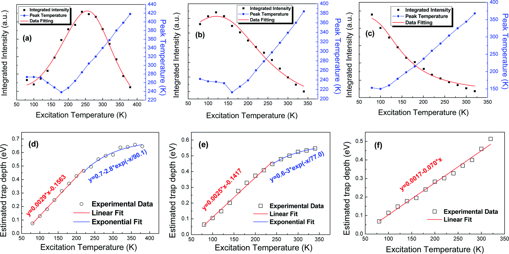
To gain more insight into the charging and detrapping behaviors of LCMSGO solid-solution phosphors, a series of elaborate TL measurements by varying the excitation temperature (Texc), accompanied by the “initial rising method” analyses, were performed on the three representative Si:Ge = 1:1, Si:Ge = 1:2, and LCMGO samples with intense afterglow, as presented in Fig. S5a, c and e (ESI†). The measurement details and the involved physical pictures have been previously elucidated by Eeckhout et al.48 For each measurement, the sample was cooled/heated to a given Texc, irradiated with 460 nm light for 5 min, delayed at a time interval of 3 min, and then measured starting from Texc at a heating rate of 1 K s−1. The 3 min delay time is used, since we found that it assures the depletion of a vast majority of unstable electrons in the traps, and the exclusion of the fast persistent decays at all excitation temperatures. Correspondingly, the trap information derived from the TL spectra reflects the trap states occupied by stable electrons at different temperatures. Upon gradually changing Texc, the number and distribution of the trapped electrons alter in a regular manner, so the TL curves measured at different Texc provide comprehensive and in-depth information of the electron charging and detrapping processes. Herein, we made a comparative study on the TL behaviors of the solid-solution phosphor for the first time, and observed some interesting phenomena. The plot of integrated TL peak intensity (Iint) as a function of Texc (Fig. 7a–c) shows clear rising and falling sections in the Si:Ge = 1:1 sample with the inflection point of 240 K; however, the rising section is reduced in the Si:Ge = 1:2 sample with the inflection point decreased to 120 K, and it totally disappears in the LCMGO sample. Assuming the concentration of electrons stored in the traps is only determined by the electron charging and detrapping processes, we tentatively fit the data of Texcversus Iint in three samples based on the formula49,50
| |  | (2) |
where
Iint(
T) is the integrated TL intensity at the excitation temperature
T,
kB is the Boltzmann constant, and
Ec and
Ed are the thermal activation energies for electron charging and detrapping, respectively. The fitted data are summarized in
Table 2. Evidently, both
Ec and
Ed decrease with the increase of Ge content, according well with the postulation that CB lowering leads to more electrons being captured by the traps and more electrons escaping from the traps. It is worth noting that
Ec and
Ed are not the real values of activation energies for electron charging and detrapping, but only serve as their rough estimations, since the severe electron retrapping process, reflected by the TL peak shifting with prolonging excitation time (Fig. S6, ESI
†), is not taken into consideration. Although these fitted values are not so exact, they can still be used to make a qualitative judgment on the variations for the relative energy position of the Ce
3+:5d excited state to the CB bottom, and that for the trap state to the CB bottom. It can be concluded that the Ce
3+:5d
1 excited state locates below the CB bottom in the Si
:
Ge = 1
:
1 and Si
:
Ge = 1
:
2 samples since the obvious thermal ionization process is observed.
11 The rising section in the plot indicates that the electron charging overwhelms the electron detrapping within the excitation temperature range. In contrast, the falling section suggests that the detrapping process is dominant. When more Ge is substituted for Si, the inflection point representing the equilibrium of electron charging and detrapping shifts toward the low temperature side and is not even observed in the LCMGO sample, which indicates that the electron detrapping tends to take control, therefore the persistent lifetime gradually shortens. The peak temperature (
Tpeak) dependent on
Texc first decreases exponentially, and, then, increases monotonically with the inflection points of 180 K (Si
:
Ge = 1
:
1), 160 K (Si
:
Ge = 1
:
2) and 100 K (LCMGO), suggesting that the excitation temperature affects the distribution of electrons in the traps.
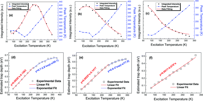 |
| | Fig. 7 Dependence of Tpeak and Iint on Texc, obtained from the TL spectra of (a) Si:Ge = 1:1, (b) Si:Ge = 1:2, and (c) LCMGO samples. Estimated trap depths in the (d) Si:Ge = 1:1, (e) Si:Ge = 1:2, and (f) LCMGO samples as a function of Texc. | |
Table 2 Fitted parameters of the samples based on the formula of eqn (2)
| Sample |
A
c
|
E
c (eV) |
A
d
|
E
d (eV) |
| Si:Ge = 1:1 |
4117.26 |
0.225 |
16.15 |
0.043 |
| Si:Ge = 1:2 |
34.69 |
0.079 |
52.53 |
0.002 |
| LCMGO |
36.81 |
0.048 |
0 |
0 |
Then, we adopted the initial rising method to estimate the trap depth and distribution, as presented in Fig. S5b, d and f (ESI†). This method is able to efficiently reveal the shallowest occupied electron trap depth in the host, regardless of the order of the kinetics involved in the detrapping processes.48,51,52 Making assumptions that the concentration of trapped electrons on the low-temperature side of a TL glow curve remains relatively constant, TL intensity (I(T)) can be approximately expressed as:48
| |  | (3) |
where
C is the constant including the frequency factor
s, and
k is the Boltzmann constant. By plotting the TL curves as ln(
I)
vs. (1000/
T), the shallowest trap depth
E can be determined by the slope of a fitted straight section at the low-temperature side. By further plotting the estimated trap depth
versus Texc (
Fig. 7d–f), the trap depth distribution can be roughly identified. One can see the good linear fit in the LCMGO sample, indicating that the detrapping rate is constant, and so it is considered to have the uniform trap depth distribution. There are two different fit functions for the Si
:
Ge = 1
:
1 and Si
:
Ge = 1
:
2 samples, probably attributed to two different kinds of traps. The shallower trap follows the uniform distribution, while the deeper one follows the exponential distribution. It is also found that the shallowest trap depth is even lower than 0.1 eV, which might be responsible for the millisecond afterglow.
3.5. PersL mechanism
According to the dependence of electron charging and detrapping on the solid-solution composition, we believe that Dorenbos’ model should be the most applicable for the PersL mechanism in LCMSGO, as schematically illustrated in Fig. 1. The blue-light pumped electrons delocalize from the Ce3+:5d1 state to the CB via photoionization, and then they are further captured by the traps; meanwhile the holes are left behind. With the thermal perturbation, the immobilized electrons gradually release from the traps and recombine with the holes to realize PersL. Bandgap engineering enables the blue-light induced electron charging and the millisecond ranged electron detrapping, making LCMSGO potential candidates for AC-LED application.
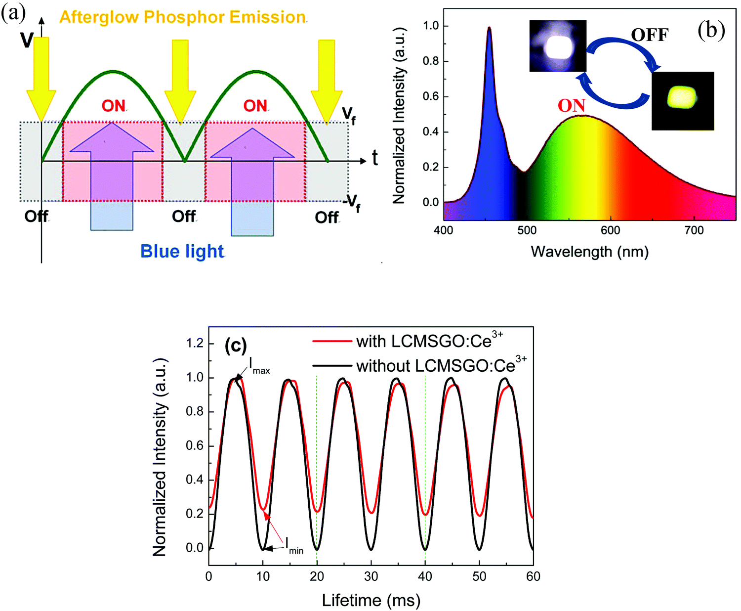
3.6. AC-LED performance
As a proof-of-concept experiment, an AC-LED prototype device was fabricated by coupling the Lu1.98CaMg2Si1Ge2O12:0.02Ce3+ based phosphor-in-silicone (PiS, made by dispersing Lu1.98CaMg2Si1Ge2O12:0.02Ce3+ phosphor in silicone) with a commercial InGaN blue-emitting chip, and connecting to an AC bridge circuit. The concept of AC flicker compensation by the PersL phosphor is presented in Fig. 8a. When the voltage across the circuit is higher than the turn-on voltage (VF) of the LED, the Lu1.98CaMg2Si1Ge2O12:0.02Ce3+ phosphor is irradiated to produce yellow light (the emitted yellow light blends with the transmitted blue light to yield white light) and, in parallel, the trap in the host stores the excitation energy. When the voltage is lower than VF, the excitation ceases and the energy stored in the traps is released to yield PersL and compensate the dimming period of the AC-LED. The typical electroluminescence spectrum of the fabricated w-LED is displayed in Fig. 8b. Upon driving with a 20 mA current, the prototype device exhibits neutral white light with a luminous efficacy of 42.8 lm W−1, CRI of 80.7, CCT of 5247 K, and a chromaticity coordinate of (0.3382, 0.3401). Percent flicker (δ), expressed as δ = 100% × (Imax − Imin)/(Imax + Imin),53 is adopted to characterize the flickering effect, where Imax and Imin represent the maximal and minimal luminescent intensities. Evidently, the AC-LED flicker is reduced from 100% to 64.1% (Fig. 8c) due to compensation arising from the stimulus intensity of the afterglow.
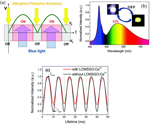 |
| | Fig. 8 (a) The strategy of using a persistent material to compensate the flicker of an AC-LED constructed with an AC bridge circuit design. (b) Electroluminescent spectrum of an AC-LED prototype device fabricated by coupling the Lu1.98CaMg2Si1.5Ge1.5O12:0.02Ce3+ based PiS composite with a commercial InGaN blue chip, under 20 mA current; insets are the luminescence photographs of the corresponding AC-LED on state and off state. (c) Luminescence intensity variation of AC-LEDs in the presence/absence of the LCMSGO:Ce3+ based PiS driven in AC periodic cycles. | |
4. Conclusion
In summary, we report a new kind of garnet persistent phosphors, Lu2CaMg2(Si1−xGex)3O12:Ce3+, which feature blue light activated afterglow in a millisecond time window. The successful solid-solution formation is verified by microstructural analysis, including XRD Rietveld refinement and HRTEM observation. The host bandgap tailoring is found to mainly originate from the CB lowering according to the electronic structure evaluation implemented by the first-principle calculation. As revealed by the composition dependent spectroscopic measurements, not only the crystal field around Ce3+ is varied, but also the PersL properties can be greatly altered upon changing the Ge:Si ratio. The presence of the trapped electrons in the host is confirmed and the trap type is designated by EPR as the Ge-related defect species. The TL measurements accompanied by “initial rising method” analyses were performed to take a closer look at the electron charging and detrapping processes, unraveling relationships between the host bandgap, the trap depth and distribution, and the PersL behavior. Based on the knowledge of electron charging and detrapping, the Dorenbos model is believed appropriate for the PersL mechanism in the LCMSGO:Ce3+ solid-solution phosphors. As a proof-of-concept experiment, an AC-LED prototype device is fabricated by coupling Lu1.98CaMg2Si1Ge2O12:0.02Ce3+ with an InGaN blue-emitting chip, and connected to an AC bridge circuit, which shows a reduced percent flicker of 64.1%.
Acknowledgements
This work was supported by the National Natural Science Foundation of China (11574312, 51472242, 11304312, 11674318) and The National Key Research and Development Program of China (2016YFB0701003).
References
- X. H. Zhang, L. Y. Li, J. Su, Y. M. Wang, Y. L. Shi, X. L. Ren, N. S. Liu, A. Q. Zhang, J. Zhou and Y. H. Gao, Laser Photonics Rev., 2014, 8, 429–435 CrossRef CAS.
- H. Y. Ye, W. Q. Liao, C. L. Hu, Y. Zhang, Y. M. You, J. G. Mao, P. F. Li and R. G. Xiong, Adv. Mater., 2016, 28, 2579–2586 CrossRef CAS PubMed.
- Z. G. Xia, C. G. Ma, M. S. Molokeev, Q. L. Liu, K. Rickert and K. R. Poeppelmeier, J. Am. Chem. Soc., 2015, 137, 12494–12497 CrossRef CAS PubMed.
- W. J. Yang, B. D. Liu, B. Yang, J. Y. Wang, T. Sekiguchi, S. Thorsten and X. Jiang, Adv. Funct. Mater., 2015, 25, 2543–2551 CrossRef CAS.
- J. Arbiol, M. de la Mata, M. Eickhoff and A. F. I. Morral, Mater. Today, 2013, 16, 213–219 CrossRef CAS.
- J. M. Klostranec and W. C. W. Chan, Adv. Mater., 2006, 18, 1953–1964 CrossRef CAS.
- J. H. Kim and P. H. Holloway, Adv. Mater., 2005, 17, 91–96 CrossRef CAS.
- T. Kuykendall, P. Ulrich, S. Aloni and P. Yang, Nat. Mater., 2007, 6, 951–956 CrossRef CAS PubMed.
- A. Kongkanand, K. Tvrdy, K. Takechi, M. Kuno and P. V. Kamat, J. Am. Chem. Soc., 2008, 130, 4007–4015 CrossRef CAS PubMed.
- J. Ueda, K. Kuroishi and S. Tanabe, Appl. Phys. Lett., 2014, 104, 101904 CrossRef.
- J. Ueda, P. Dorenbos, A. J. J. Bos, K. Kuroishi and S. Tanabe, J. Mater. Chem. C, 2015, 3, 5642–5651 RSC.
- J. Ueda, P. Dorenbos, A. J. J. Bos, A. Meijerink and S. Tanabe, J. Phys. Chem. C, 2016, 120, 5916–5921 Search PubMed.
- H. D. Luo, A. J. J. Bos and P. Dorenbos, J. Phys. Chem. C, 2016, 120, 5916–5925 CAS.
- B. Wang, H. Lin, Y. L. Yu, D. Q. Chen, R. Zhang, J. Xu and Y. S. Wang, J. Am. Ceram. Soc., 2014, 97, 2539–2545 CrossRef CAS.
- Y. Li, Y. Y. Li, R. C. Chen, K. Sharafudeen, S. F. Zhou, M. Gecevicius, H. H. Wang, G. P. Dong, Y. L. Wu, X. X. Qin and J. R. Qiu, NPG Asia Mater., 2015, 7, e180 CrossRef.
- Y. Li, M. Gecevicius and J. R. Qiu, Chem. Soc. Rev., 2016, 45, 2090–2136 RSC.
- Z. W. Pan, Y. Y. Lu and F. Liu, Nat. Mater., 2012, 11, 58–63 CrossRef CAS PubMed.
- J. T. Piegza, J. Niittykoski, J. Hölsä and E. Zych, Chem. Mater., 2008, 20, 2252–2261 CrossRef.
- B. Y. Qu, B. Zhang, L. Wang, R. L. Zhou and X. C. Zeng, Chem. Mater., 2015, 27, 2195–2202 CrossRef CAS.
- K. van den Eeckhout, P. F. Smet and D. Poelman, Materials, 2010, 3, 2536–2566 CrossRef CAS.
- T. Matsuzawa, Y. Aoki, N. Takeuchi and Y. Murayama, J. Electrochem. Soc., 1996, 143, 2670–2673 CrossRef CAS.
- P. Dorenbos, J. Electrochem. Soc., 2005, 152, H107–H110 CrossRef CAS.
- D. D. Jia, X. J. Wang and W. M. Yen, Phys. Rev. B: Condens. Matter Mater. Phys., 2004, 69, 235113 CrossRef.
- G. F. J. Garlick and M. H. F. Wilkins, Proc. R. Soc. London, Ser. A, 1945, 184, 408 CrossRef CAS.
- T. Kanai, M. Satoh and I. Miura, J. Am. Ceram. Soc., 2008, 91, 456–462 CrossRef CAS.
- C. W. Yeh, Y. Li, J. Wang and R. S. Liu, Opt. Express, 2012, 20, 18031–18034 CrossRef CAS PubMed.
- L. Chen, Y. Zhang, F. Y. Liu, A. Q. Luo, Z. X. Chen, Y. Jiang, S. F. Chen and R. S. Liu, Mater. Res. Bull., 2012, 47, 4071–4075 CrossRef CAS.
- L. Chen, Y. S. Zhang, C. Xue, X. R. Deng, A. Q. Luo, F. Y. Liu and Y. Jiang, Funct. Mater. Lett., 2013, 6, 1350047 CrossRef.
- H. Lin, B. Wang, J. Xu, R. Zhang, H. Chen, Y. L. Yu and Y. S. Wang, ACS Appl. Mater. Interfaces, 2014, 6, 21264–21269 CAS.
- H. Lin, J. Xu, Q. M. Huang, B. Wang, H. Chen, Z. B. Lin and Y. S. Wang, ACS Appl. Mater. Interfaces, 2015, 7, 21835–21843 CAS.
- A. A. Setlur, W. J. Heward, Y. Gao, A. M. Srivastava, R. G. Chandran and M. V. Shankar, Chem. Mater., 2006, 18, 3314–3322 CrossRef CAS.
- Y. R. Shi, G. Zhu, M. Mikami, Y. Shimomura and Y. H. Wang, Dalton Trans., 2015, 44, 1775–1781 RSC.
- W. Kohn, Rev. Mod. Phys., 1999, 71, 1253–1266 CrossRef CAS.
- S. J. Clark, M. D. Segall, C. J. Pickard, P. J. Hasnip, M. J. Probert, K. Refson and M. C. Payne, Z. Kristallogr., 2005, 220, 567–570 CAS.
- J. P. Perdew, K. Burke and M. Ernzerhof, Phys. Rev. Lett., 1996, 77, 3865–3868 CrossRef CAS PubMed.
- H. J. Monkhorst and J. D. Pack, Phys. Rev. B: Solid State, 1976, 13, 5188–5192 CrossRef.
- D. Vanderbilt, Phys. Rev. B: Condens. Matter Mater. Phys., 1990, 41, 7892–7895 CrossRef.
- B. G. Pfrommer, M. Cote, S. G. Louie and M. L. Cohen, J. Comput. Phys., 1997, 131, 233–240 CrossRef CAS.
- Y. H. Li, A. Walsh, S. Y. Chen and S. H. Wei, Appl. Phys. Lett., 2009, 94, 212109 CrossRef.
- S. H. Wei. and A. Zunger, Phys. Rev. Lett., 1987, 59, 144–147 CrossRef CAS PubMed.
- P. Dorenbos, J. Phys.: Condens. Matter, 2013, 25, 225501 CrossRef PubMed.
- S. Agnello, A. Alessi, F. M. Gelardi, R. Boscaino, A. Parlato, S. Grandi and A. Magistris, Eur. Phys. J. B, 2008, 61, 25–31 CrossRef CAS.
- N. Chiodini, F. Meinardi, F. Morazzoni, A. Paleari and R. Scotti, Phys. Rev. B: Condens. Matter Mater. Phys., 1999, 60, 2429–2435 CrossRef CAS.
- L. Giacomazzi, L. Martin-Samos, A. Boukenter, Y. Ouerdane, S. Girard and N. Richard, Opt. Mater. Express, 2005, 5, 1054–1064 CrossRef.
- L. Zhang, C. Y. Li, S. B. Wang and Q. Su, J. Lumin., 2007, 126, 551–555 CrossRef CAS.
- R. Pang, Y. L. Jia, R. Zhao, H. F. Li, J. P. Fu, W. Z. Sun, L. H. Jiang, S. Zhang, C. Y. Li and Q. Su, Dalton Trans., 2014, 43, 9661–9668 RSC.
- P. Dorenbos, J. Phys.: Condens. Matter, 2005, 17, 8103–8111 CrossRef CAS.
- K. van den Eeckhout, Adrie J. J. Bos, D. Poelman and P. F. Smet, Phys. Rev. B: Condens. Matter Mater. Phys., 2013, 87, 045126 CrossRef.
- T. Arai and S. Adachi, J. Lumin., 2014, 153, 46–53 CrossRef CAS.
- J. T. Kong, W. Zheng, Y. S. Liu, R. F. Li, E. Ma, H. M. Zhu and X. Y. Chen, Nanoscale, 2015, 7, 11048–11054 RSC.
-
S. W. S. McKeever, Thermoluminescence of Solid, Cambridge University Press, Cambridge, UK, 1985 Search PubMed.
- A. J. J. Bos, Radiat. Meas., 2007, 41, S45–S56 CrossRef CAS.
-
M. S. Rea, The IESNA Lighting Handbook, Illuminating Engineering Society, New York, 2007 Search PubMed.
Footnote |
| † Electronic supplementary information (ESI) available. See DOI: 10.1039/c6tc03818b |
|
| This journal is © The Royal Society of Chemistry 2016 |
Click here to see how this site uses Cookies. View our privacy policy here. 
 Open Access Article
 This Open Access Article is licensed under a