
 Open Access Article
 This Open Access Article is licensed under a
 Creative Commons Attribution 3.0 Unported Licence
Synthesis and photoluminescence properties of a phase pure green-emitting Eu doped JEM sialon (LaSi6−zAl1+zN10−zOz, z ∼ 1) phosphor with a large red-shift of emission and unusual thermal quenching behavior
Chun-Yun
Wang
*ab,
Takashi
Takeda
*ab,
Otmar Melvin
ten Kate
b,
Rong-Jun
Xie
b,
Kohsei
Takahashi
b and
Naoto
Hirosaki
b
aGraduate School of Chemical Sciences and Engineering, Hokkaido University, Sapporo 060-8628, Japan. E-mail: WANG.Chunyun@nims.go.jp; TAKEDA.Takashi@nims.go.jp
bSialon Group, National Institute for Materials Science (NIMS), Namiki 1-1, Tsukuba, Ibaraki 305-0044, Japan
First published on 3rd October 2016
Abstract
A green-emitting phosphor, Eu2+ doped LaAl(Si6−zAlz)(N10−zOz) (denoted as JEM, z ∼ 1), was synthesized via a solid-state reaction method. By the careful control of the sintering temperature and chemical composition of starting materials (z value, N/O ratio and Si/Al ratio), a single phase JEM phosphor was achieved for the first time. The JEM:Eu2+ phosphor displays a broad 4f–5d excitation band from the UV region up to 525 nm, with a maximum at 355 nm. Excitation at 355 nm results in a Eu2+ 5d–4f emission band, that shows a large red-shift (490 → 564 nm) and a change in shape with increasing Eu concentration. The thermal quenching behavior of JEM:Eu2+ has been investigated in the temperature range from 4 K to 573 K. An abnormal nearly linear relation is observed between temperature and luminescence intensity. These phenomena indicate that there are two types of Eu2+ sites, although only one crystallographic site can be found in the JEM structure. A non-linear decay behavior with a bi-exponential curve and time-resolved photoluminescence emission spectra with two distinctive Gaussian peaks further give strong evidence for two emission sites in the Eu2+ doped JEM phosphor.
Introduction
In recent decades, oxy-nitride phosphors have received great attention due to their large flexibility in tuning the photoluminescence spectra, high conversion efficiency, small thermal quenching and high chemical stability. Especially rare earth ion activated nitrido-silicate phosphors, M–Si–(Al)–(O)–N:RE (M is an alkaline earth or lanthanide metal, RE is a rare earth ion), possess a strong covalent and highly condensed structure built up on a corner or edge sharing SiN4 tetrahedral framework, which leads to flexible controlling of photoluminescence spectra and structural diversity and stability.1–4 Furthermore, the structural variety of nitrido-silicates can be further extended by substituting Si with Al or Li resulting in nitridoalumino- or nitridolithosilicates, respectively.5–7 Several efficient phosphors promising for application in white light-emitting diodes (LEDs) have been discovered among the nitrido-silicate phosphors, such as (1) blue-emitting phosphors: LaAl(Si6−zAlz)N10−zOz:Ce3+8 and Ca-α-sialon:Ce3+ (Cam/2Si12−(m+n)Alm+nOnN16−n:Ce3+);9 (2) green-emitting phosphors: β-sialon:Eu2+ (Si6−zAlzOzN8−z:Eu2+),10 SrSi2O2N2:Eu2+,11 and Ba2LiSi7AlN12:Eu2+;12 (3) yellow-emitting phosphors: Ca-α-sialon:Eu2+13 and Li-α-sialon:Eu2+ (LimSi12−(m+n)Alm+nOnN16−n:Eu2+);14 (4) red-emitting phosphors: Sr2Si5N8:Eu2+,15 CaAlSiN3:Eu2+,16 and Sr(LiAl3N4):Eu2+.17 However, the number of commercialized rare earth ion activated nitrido-silicate phosphors is very limited due to some problems, such as quantum efficiency, cost, spectral shape, large thermal quenching and degradation, the difficulty to get phase pure powder samples and so on. For instance, SrSi2O2N2:Eu2+ has a higher quantum efficiency than β-sialon:Eu2+, but it suffers from large thermal degradation due to its layer structure, which makes the Eu2+ easy to oxidize.18LaAl(Si6−zAlz)(N10−zOz) (denoted as JEM, z ∼ 1) was discovered as an intergranular phase in ceramic materials by Grins et al. in 1995.19 JEM has an orthorhombic structure with lattice parameters a = 9.4303 Å, b = 9.7689 Å, and c = 8.9386 Å in space group Pbcn. The Al atoms and (Si,Al) atoms are tetrahedrally coordinated by (N,O) atoms, yielding an Al(Si,Al)6(N,O)103− network. The La atoms are located in the tunnels formed by the network extending along the [001] direction and are irregularly coordinated by seven (N,O) atoms at an average distance of 2.70 Å.19 It was mainly studied as a heat-resistant material until 2007 when Takahashi et al.8 reported that a Ce doped JEM phase phosphor can emit blue light with high quantum efficiency (internal quantum efficiency is around 62%) after 405 nm light excitation. Its emission spectra peak wavelength is widely tunable in a range of 460–500 nm, and a high color rendering index (Ra = 95–96) has been obtained for the near-UV LED with various correlated color temperatures. Therefore, JEM:Ce3+ has been strongly suggested as a candidate for solid-state lighting, especially for home illumination. Afterwards, the photoluminescence properties of the JEM:Ce3+ phosphor were enhanced by co-doping Ca.20 However, a phase pure JEM phosphor has not yet been obtained, with some impure phases even coexisting inside the same particle.21 In general, Eu2+ and Ce3+ are the two most effective and frequently used activators in LED phosphors due to their flexibility to control and tailor the photoluminescence properties. However, the properties of Eu2+ doped JEM phosphors have not been reported at present.
In this work, we report the synthesis of a Eu doped JEM phosphor by using La2O3, LaN, Si3N4, AlN and Eu2O3 as starting materials. Aiming at a phase pure JEM:Eu phosphor, the effects of the synthesis temperature and chemical composition of the starting materials (z value, N/O ratio and Si/Al ratio) are investigated. After getting the Eu doped single phase JEM sample, we further investigate the photoluminescence properties of the JEM:Eu phosphor.
Experimental section
1. Sample preparation
Eu2+ doped LaAl(Si6−zAlz)(N10−zOz) (z ∼ 1) phosphor powder samples were prepared via a solid-state reaction method. Appropriate amounts of starting materials including La2O3 (Shin-Etsu Chemical Co.), LaN, α-Si3N4 (SN-E10, Ube Industries), AlN (Tokuyama, E-grade) and Eu2O3 (Shin-Etsu Chemical Co.) powders were weighed with designed chemical compositions and then packed in boron nitride crucibles in a glove box filled with nitrogen gas. The samples were fired in a nitrogen gas-pressure sintering furnace (Fujidempa Kogyo Co. Ltd, Osaka, Japan) at 1800–1900 °C for 2 hours. After heating, the sintered samples were finely ground using a mortar for further characterization.2. Characterization
The crystalline phases of the samples were detected with X-ray powder diffraction (XRD) by using Cu Kα1 radiation (Rigaku, Smartlab). The quantitative analysis of the crystalline phases was conducted using a reference intensity ratio (RIR) method.22 A field-emission scanning electron microscope (Hitachi S4800) was used to investigate the microstructure of the samples. Photoluminescence spectra at room temperature were measured using a spectrophotometer (Hitachi F-4500) equipped with a Xe lamp. The diffuse reflectance spectra were recorded using a UV/vis spectrophotometer (JASCO, V-560), and a Spectralon resin was used for calibration.23 X-Ray absorption of the Eu-LIII edge was measured by the transparent method with the beam line BL9C (Photo Factory, KEK, Japan). Low temperature dependent luminescence spectra were recorded using a spectrometer (Otsuka electronics, MCPD-9800) and a Xe lamp. Samples were cooled from 298 K to 4 K by using a He cryostat (Oxford, OPTICOOL). Luminescence spectra above room temperature were obtained using a multichannel detector (Otsuka electronics, MCPD-7000) under excitation at 355 nm from 298 K to 573 K. This measurement system combined with an integrating sphere was also used to measure the emission and reflectance of the phosphors for calculating the internal quantum efficiency (IQE) according to the formula:24where E(λ), R(λ) and P(λ) are the intensity per unit wavelength in the spectra of excitation, reflectance, and emission of the phosphor, respectively. Luminescence decay and time-resolved photoluminescence emission spectra at room temperature were measured by a time-correlated single photon counting system (TCSPC) technique, using a 370 nm and 1.2 ns pulse duration nanoLED as the excitation source (Horiba Jobin Yvon, FluoroCube).
Results and discussion
1. Phase identification and microstructure
Grins et al.19 reported the first synthesis of the LaAl(Si6−zAlz)(N10−zOz) (JEM, z ∼ 1) phase material with an overall composition of La2Al4Si11N18O4 synthesized at 1800 °C, containing 31.7% β-sialon as an impurity phase. Takahashi et al.8 synthesized Ce doped JEM phosphor La1−xCexSi6−zAl1+zOzN10−z (z = 1) at 1900 °C by using α-Si3N4, AlN, La2O3 and CeO2 as the starting materials. The JEM phase content reached 94% in the case of x < 0.5. However, β-sialon (Si6−zAlzOzN8−z) was still present as the only secondary phase. Afterwards, Takahashi et al.21 tried to enhance the phase purity of JEM by setting the z value to 1.5 and a synthesis temperature of 1800 °C. Yet a very small amount of La N-phase (La3Si6.5Al1.5N9.5O5.5) formed, while β-sialon could also be detected. Some impure phases even coexisted inside one particle. Based on these previous works, it is believed that the temperature and chemical composition play a key role in JEM phase formation. However, there is no report in the literature about the effect of temperature and chemical composition on JEM phase formation.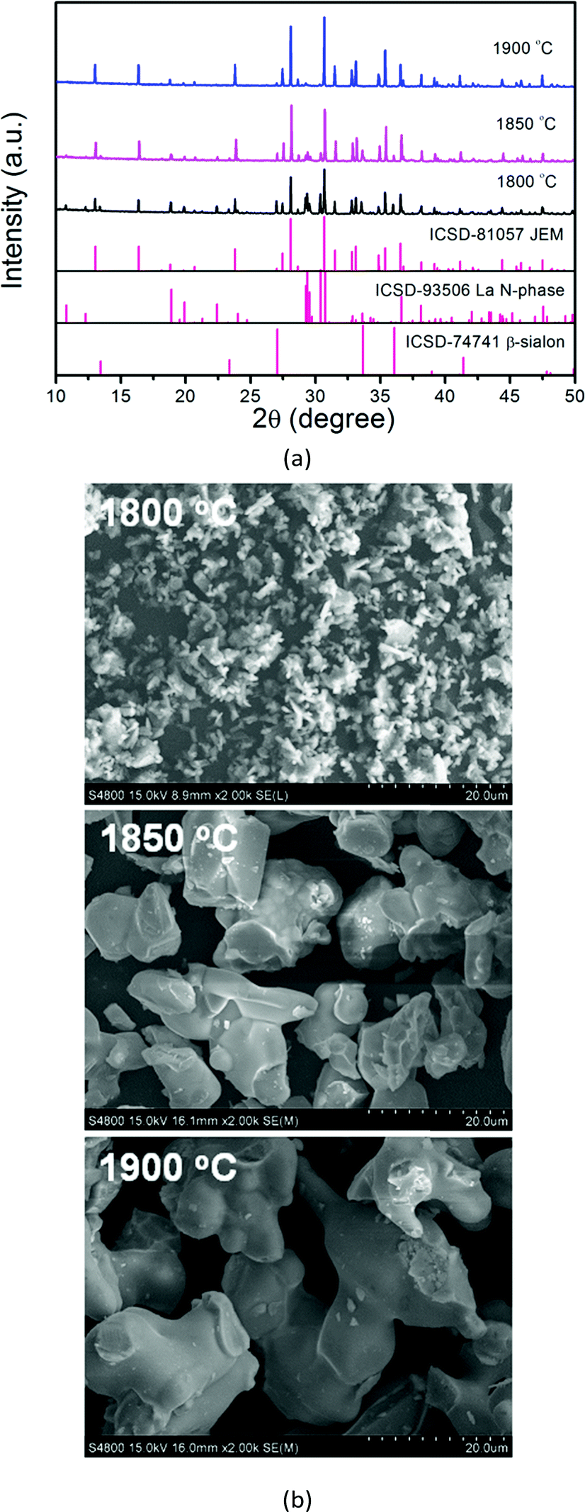 | ||
| Fig. 1 XRD patterns (a) and SEM images (b) of La1−xEuxSi6−zAl1+zOzN10−z (z = 1, x = 0.05) samples sintered at 1800 °C, 1850 °C and 1900 °C. | ||
The sample synthesized at 1900 °C seems to contain the least amount of impurity (β-sialon) based on the XRD pattern. However, the SEM images of the samples shown in Fig. 1b display that the particles of the sample synthesized at 1900 °C contain a glassy surface, which is probably caused by some melting of the JEM phase during the synthesis. The particles of the sample synthesized at 1850 °C are much rougher and do not have the glassy surface. It is therefore believed that the JEM phase could better be synthesized at 1850 °C in order to prevent melting of the surface of the particles.
(1) z value effect. The target samples, 5% Eu doped JEM (La1−xEuxSi6−zAl1+zOzN10−z, x = 0.05) with different z values (z = 1.00, 1.12, 1.25, 1.31, 1.50), were weighed according to the molar ratios of each starting material listed in Table 1 (samples No. 1–5) and fired at 1850 °C for 2 hours. The XRD patterns of the samples are shown in Fig. 2a. The main phase is the JEM phase. However, all samples also contain the La N-phase as an impurity phase, as well as a small amount of β-sialon, except for the samples with z = 1.12 and 1.25 in which no beta-sialon is present. It should be noted that varying the z value does not lead to a significant change in the lattice parameters of the main phase, suggesting that a monophasic JEM sample might be achieved with a specific z value or a very narrow region of z values. By comparing the chemical composition of the crystalline phases (JEM, La N-phase and β-sialon), it is found that all of them are sialon phase materials but with different Si/Al and N/O ratios. It is therefore believed that the Si/Al and N/O ratios of the starting materials play a key role in the phase purity of JEM. The adjustment of the z value changes simultaneously the N/O ratio as well as the Si/Al ratio, as shown by the black line in the composition map of Fig. 2b. It should be noted that the N/O ratio of the starting materials might in reality be different from that suggested by the ratios in Table 1, since Si3N4 and AlN that were used probably contain some oxygen impurity. In addition, when Eu2+ ions substitute for La3+ ions, the charge compensation may affect the distribution of Si/Al and N/O. These might be the reasons for the difficulty in obtaining a single JEM phase by just changing the z value.
| No. | z value | Si/Al ratio | N/O ratio | La2O3 | LaN | Si3N4 | AlN | Eu2O3 |
|---|---|---|---|---|---|---|---|---|
| 1 | 1.00 | 2.50 | 8.33 | 0.32 | 0.32 | 1.67 | 2.00 | 0.025 |
| 2 | 1.12 | 2.30 | 7.39 | 0.36 | 0.24 | 1.63 | 2.12 | 0.025 |
| 3 | 1.25 | 2.11 | 6.57 | 0.40 | 0.16 | 1.58 | 2.25 | 0.025 |
| 4 | 1.31 | 2.03 | 6.24 | 0.42 | 0.12 | 1.56 | 2.31 | 0.025 |
| 5 | 1.50 | 1.80 | 5.37 | 0.48 | 0 | 1.50 | 2.50 | 0.025 |
| 6 | 2.50 | 9.00 | 0.31 | 0.33 | 1.67 | 2.00 | 0.025 | |
| 7 | 2.50 | 8.33 | 0.32 | 0.32 | 1.67 | 2.00 | 0.025 | |
| 8 | 2.50 | 7.74 | 0.36 | 0.23 | 1.67 | 2.00 | 0.025 | |
| 9 | 2.50 | 7.22 | 0.38 | 0.18 | 1.67 | 2.00 | 0.025 | |
| 10 | 2.50 | 6.77 | 0.41 | 0.13 | 1.67 | 2.00 | 0.025 | |
| 11 | 2.50 | 6.36 | 0.43 | 0.08 | 1.67 | 2.00 | 0.025 | |
| 12 | 2.50 | 6.00 | 0.45 | 0.04 | 1.67 | 2.00 | 0.025 | |
| 13 | 2.50 | 5.78 | 0.48 | 0 | 1.67 | 2.00 | 0.025 | |
| 14 | 2.50 | 6.00 | 0.45 | 0.04 | 1.67 | 2.00 | 0.025 | |
| 15 | 2.39 | 6.00 | 0.45 | 0.04 | 1.63 | 2.05 | 0.025 | |
| 16 | 2.30 | 6.00 | 0.45 | 0.04 | 1.62 | 2.11 | 0.025 | |
| 17 | 2.20 | 6.00 | 0.45 | 0.04 | 1.60 | 2.18 | 0.025 | |
| 18 | 2.11 | 6.00 | 0.45 | 0.04 | 1.58 | 2.25 | 0.025 | |
| 19 | 2.03 | 6.00 | 0.45 | 0.04 | 1.57 | 2.31 | 0.025 | |
| 20 | 1.88 | 6.00 | 0.45 | 0.04 | 1.53 | 2.45 | 0.025 | |
| 21 | 1.81 | 6.00 | 0.45 | 0.04 | 1.52 | 2.51 | 0.025 | |
| 22 | 1.12 | 2.30 | 7.93 | 0.37 | 0.25 | 1.63 | 2.12 | 0 |
| 23 | 2.30 | 6.00 | 0.48 | 0.04 | 1.62 | 2.11 | 0.0025 | |
| 24 | 2.30 | 6.00 | 0.47 | 0.04 | 1.62 | 2.11 | 0.005 | |
| 25 | 2.30 | 6.00 | 0.47 | 0.04 | 1.62 | 2.11 | 0.01 | |
| 26 | 2.30 | 6.00 | 0.45 | 0.04 | 1.62 | 2.11 | 0.025 | |
| 27 | 2.30 | 6.00 | 0.43 | 0.04 | 1.62 | 2.11 | 0.05 | |
| 28 | 2.30 | 6.00 | 0.38 | 0.04 | 1.62 | 2.11 | 0.10 |
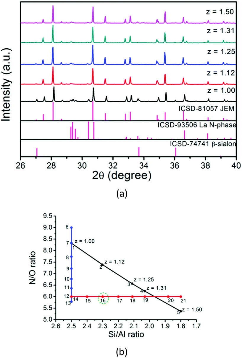 | ||
| Fig. 2 (a) XRD patterns of 5% Eu doped JEM samples La1−xEuxSi6−zAl1+zOzN10−z with different z values (x = 0.05, z = 1.00, 1.12, 1.25, 1.31, 1.50); (b) chemical composition map of the N/O and Si/Al ratios according to the starting materials. The black line presents the change in the z value; the blue line shows the change in the N/O ratio with the Si/Al ratio fixed at 2.50; the Si/Al ratio was tuned as shown by the red line with the N/O ratio fixed at 6.00. The number of each point stands for the sample number that is listed in Table 1 (samples No. 1 and 7 and samples No. 12 and 14 have the same chemical composition). | ||
(2) N/O and Si/Al ratio effect. Since changing the value of z in LaSi6−zAl1+zOzN10−z does not result in a pure sample, it is suggested that a pure JEM phase sample might be obtained if the sample composition does not follow the La1−xEuxSi6−zAl1+zOzN10−z (x = 0.05) formula which is shown on the black line but lies at another position in the composition map of Fig. 2b. The Si/Al ratio was therefore fixed at 2.50, and samples with various N/O ratios were made by changing the amount of La2O3 and LaN while maintaining the amount of La constant, as shown by the blue line in Fig. 2b. The chemical composition of the samples (samples No. 6–13) is listed in Table 1.
Fig. 3a shows that the JEM phase purity is improved by decreasing the N/O ratio. The La N-phase impurity disappears when the N/O ratio is 6.00, with only β-sialon left as a secondary phase. When the N/O ratio is 5.78 (sample No. 13), no LaN is added as a starting material and the La N-phase impurity appears again. By analyzing the phase percentages of the samples with different N/O ratios, as shown in Fig. 3b, it is found that an oxygen rich composition can enhance the phase purity of JEM if the Si/Al ratio is fixed at 2.50. As β-sialon still coexisted with the JEM phase when the N/O ratio is 6.00, the Si/Al ratio was tuned by changing the amount of Si3N4 and AlN and keeping the N/O ratio at 6.00 as shown by the red line in Fig. 2b. The molar ratios of the starting materials are shown in Table 1 (samples No. 14–21).
 | ||
| Fig. 3 (a) XRD patterns of JEM:Eu samples with different N/O ratios (N/O = 9.00, 8.33, 7.22, 6.00, 5.78) and (b) quantitative analysis of phases for samples with various N/O ratios. | ||
When the N/O ratio is maintained at a value of 6.00, the JEM phase purity is significantly improved by changing the Si/Al ratio, as shown in Fig. 4, especially for samples with Si/Al = 2.30, 2.11 and 2.20, in which the amount of La N-phase is less than 1%. So carefully controlling the Si/Al ratio is very important to remove the β-sialon impurity phase. Fig. 4a shows that a single phase JEM phosphor is obtained for the sample with Si/Al = 2.30 and N/O = 6.00 (sample No. 16). The chemical composition is also marked with a green circle in Fig. 2b, deviating slightly from the formula of JEM sialon with z = 1.12 (sample No. 2).
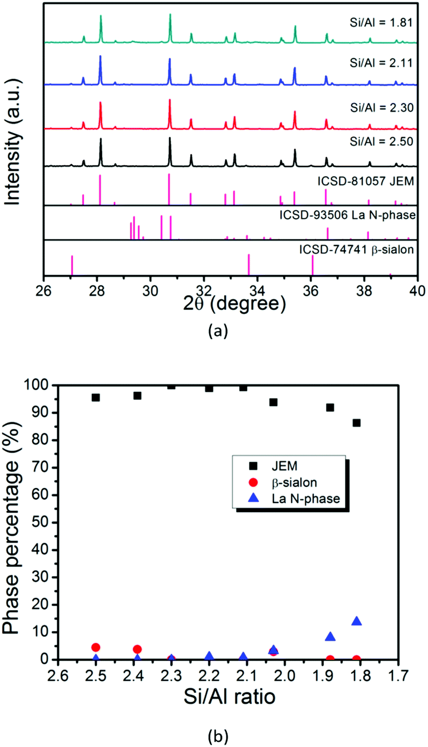 | ||
| Fig. 4 (a) XRD patterns of samples with different Si/Al ratios (Si/Al = 2.50, 2.30, 2.11, 1.81) and (b) quantitative analysis of phases for samples with various Si/Al ratios. | ||
2. Photoluminescence properties
The JEM:xEu (x = 0.005, 0.01, 0.02, 0.05, 0.10, 0.20) samples (samples No. 23–28) were weighed with the ratios of N/O = 6.00 and Si/Al = 2.30, as this is the optimal composition to get a single phase according to the experiments mentioned above. It should be noticed that no impure phase can be detected for all samples regardless of the Eu concentration. The variable occupancy of the rare earth site should be considered in the detailed structure analysis. For the non-doped JEM sample, when a sample was prepared with the optimal ratios of N/O = 6.00 and Si/Al = 2.30, a little bit of the La N-phase was observed; the proper composition to reach a single non-doped JEM sample (sample No. 22) is N/O = 7.93 and Si/Al = 2.30, and the corresponding z value is 1.12; this again indicates that precise composition control is important to obtain a single phase JEM. The molar ratio of each sample is listed in Table 1 (samples No. 22–28). Their photoluminescence properties are further investigated. | ||
| Fig. 5 Diffuse reflectance spectra of JEM:xEu samples with various Eu concentrations (x = 0, 0.005, 0.01, 0.02, 0.05, 0.10, 0.20). | ||
The Eu LIII edge XANES spectrum of JEM:0.05Eu is shown in Fig. 6 together with the reference spectra of EuCl2 and Eu2O3. The absorption edge of JEM:0.05Eu is located at 6973 eV and coincides with the Eu2+ reference position from EuCl2. There is no trace of Eu3+ in the JEM:0.05Eu sample, which further confirms that all the Eu ions in the JEM:0.05Eu phosphor are divalent. This is due to carbon heating at high temperature, which can provide a reductive atmosphere.25
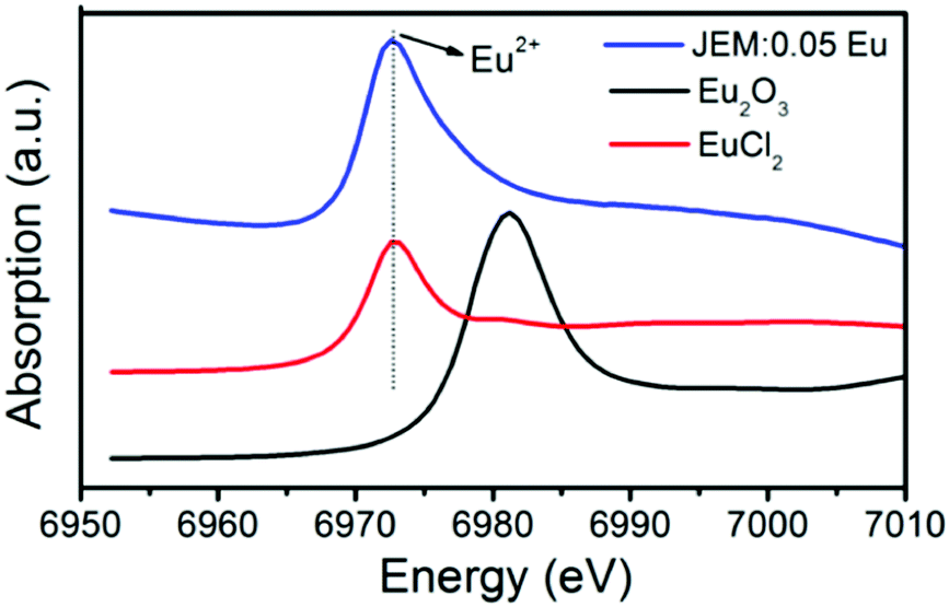 | ||
| Fig. 6 Eu LIII XANES spectra of the JEM:0.05Eu phosphor and Eu2O3, EuCl2 referenced samples for Eu3+, Eu2+, respectively. | ||
 | ||
| Fig. 7 JEM:xEu (x = 0.005, 0.01, 0.02, 0.05, 0.10, 0.20) samples as measured and normalized excitation spectra (a); emission spectra after 355 nm excitation and luminescence photos of the samples excited by a 365 nm UV lamp (b); normalized emission intensity and FWHM (c). The excitation spectra were monitored with the emission peak wavelength. | ||
The JEM structure has only one La site on which the Eu2+ can substitute and La atoms statistically occupy the 8(d) site.19 In addition, the La atoms are found to be irregularly coordinated by seven anions in the JEM structure and the charge compensation makes the coordination environment of Eu2+ very complicated. Therefore, a variety of local structures around Eu2+ give rise to inhomogeneous broadening, which makes the emission bandwidth of JEM:Eu2+ relatively large. A similar case has been observed for the CaAlSiN3:Eu2+ phosphor, for which it was reported that the inhomogeneous broadening originates from the random distribution of Si and Al ions at an identical crystal site.26
Another interesting characteristic of the JEM:Eu samples is the unusual large red-shift (490 → 564 nm) of the emission band that is observed with the increase of the Eu concentration, implying that the luminescence properties of the JEM:Eu2+ phosphor can be tailored by controlling the Eu concentration. Fig. 8 shows that the emission band of the low concentrated samples is asymmetrical, and can be fitted with two Gaussian curves, which represent high and low energy emission bands. This suggests that there are at least two types of Eu2+ sites; one site gives rise to the higher energy emission band and the other site gives rise to the lower energy emission band. Note that, when x is 0.10, the emission spectrum almost solely consists of the band at longer wavelength, as shown in Fig. 8.
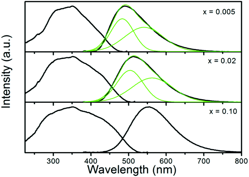 | ||
| Fig. 8 Excitation spectra and Gaussian fitting of emission spectra for samples JEM:xEu (x = 0.005, 0.02, 0.10) after 355 nm excitation. | ||
It is suggested that the main reason for the red shift at lower concentration is different from that at higher concentration. At low concentrations the redshift is mainly caused by a change in the distribution of the Eu2+ ions over the two sites. Eu2+ ions may prefer to occupy the high energy site, which results in a relatively large contribution of the emission at shorter wavelengths. This can be seen from the intensity of the shorter wavelength emission band, which is higher than that of the longer wavelength emission band when the Eu concentration is below 2%. With increasing Eu concentration also the lower energy site will be occupied more, causing a redshift of the emission. A similar explanation has also been reported for La2.5Ca1.5Si12O4.5N6.5:Eu2+.27 Upon further increasing the Eu concentration, the red-shift of the emission is further enhanced by energy transfer among Eu2+ ions. With increasing Eu concentration the average distance between the Eu2+ ions becomes shorter, increasing the probability of energy transfer from Eu2+ ions at the high energy site towards Eu2+ ions at the low energy site. Hence, the increase of the possibility of non-radiative energy transfer between Eu ions at different sites causes a red-shift of the emission band. This can also be confirmed from Fig. 8 where the relative intensity of the shorter wavelength emission band becomes lower with increasing Eu concentration and the shorter wavelength emission band almost disappears when the Eu concentration reaches 10%. A similar case was also observed in La2.5Ca1.5Si12O4.5N6.5:Eu2+![[thin space (1/6-em)]](https://www.rsc.org/images/entities/char_2009.gif) 27 and Lu3Al5O12:Ce3+.28
27 and Lu3Al5O12:Ce3+.28
It should be noted that, due to the partial overlap of emission and excitation spectra, the reabsorption of high-energy emitted photons also contributes to the red-shift. In addition, a lowering of the 5d level further enhances the red-shift with the increase of Eu concentration. The latter two effects are commonly observed in Eu2+ doped samples. However, they cannot by itself account for the very large red-shift (490 → 564 nm) and changes in the emission spectrum that are observed with increasing Eu concentration, which can only be fully explained by also taking energy transfer between Eu2+ ions at different sites into account.
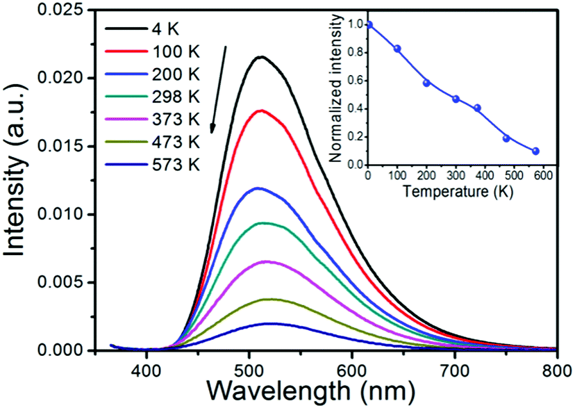 | ||
| Fig. 9 Emission spectra of the JEM:0.02Eu sample at different temperatures after 355 nm excitation. The inset shows the integrated emission intensity as a function of temperature for the sample, relative to the maximum intensity at 4 K. | ||
In general, the quenching of the 5d → 4f luminescence of Eu2+ is explained by either thermally activated cross-over from the 4f65d excited state to the 4f7 ground state, or the thermal ionization from the 4f65d excited state to the bottom of the conduction band.29,30 The Stokes shift is estimated at 0.23 eV by taking twice the energy difference between the zero phonon line energy and the energy of the emission peak.31 Given the relatively small Stokes shift and low thermal quenching temperature, the thermal quenching is more likely due to the thermal ionization from the 5d level to the conduction band, as this has also been suggested as the reason for thermal quenching in other Eu2+ doped nitrido-silicates.30,32
Note however that there is a noticeable feature of the JEM phosphor as the luminescence intensity of JEM:Eu shows a much more gradual decrease with increasing temperature; although the luminescence already starts to quench around 4 K, there is still 10% of the luminescence left around 573 K. It is noticed that this slow quenching behavior is due to multiple competitive relaxation processes. One possible reason is related to the two different luminescent sites in the Eu2+ doped JEM phosphor, as the two sites may have a different energy barrier for thermal quenching. The energy transfer between the two sites may also depend on the temperature and therefore influence the luminescence intensity. Furthermore, the emission band shows a slight redshift and a small change in shape with increasing temperature. These changes can also be related to the two types of emission sites in the Eu2+ doped JEM phosphor with different thermal quenching behaviors.
where I is the luminescence intensity; A1 and A2 are constants; t is the time; and τ1 and τ2 are the lifetimes for the exponential components. The double decay is strong evidence that there are at least two types of Eu2+ ions. The effective decay time τ can be calculated according to the formula:

| τ = (A1τ12 + A2τ22)/(A1τ1 + A2τ2) |
 | ||
| Fig. 10 Luminescence decay curves of JEM:xEu (x = 0.005, 0.02, 0.10) samples after 370 nm excitation, monitoring the 480 nm (red lines) and 560 nm emission (blue lines). | ||
Regarding the JEM:xEu samples with x = 0.005, 0.02, 0.10, the calculated effective decay times are 0.67 μs, 0.51 μs and 0.39 μs for the 480 nm emission, and 1.05 μs, 1.15 μs and 1.02 μs respectively, which are close to the typical value of Eu2+ decay.34 For all concentrations, the 480 nm emission shows faster decay than the 560 nm emission, indicating that the decay related to the high energy site is faster than the decay associated with the low energy sites. The decay time for the 560 nm emission initially increases with rising Eu concentration, which is due to the energy transfer from the high energy Eu2+ site to the low energy Eu2+ site, as the high energy Eu2+ sites with faster decay have a larger contribution to the emission of the low Eu concentrated samples. For the high Eu concentrated sample, concentration quenching leads to a shorter decay.
In order to further confirm that there are two types of Eu2+ emission sites, time-resolved photoluminescence emission spectra are measured as shown in Fig. 11. Each time-resolved photoluminescence emission spectrum contains two distinctive Gaussian peaks, which confirms the existence of the two luminescent centers. The intensity of the high energy component reduces upon increasing the delay time, which is in agreement with the observation that the short monitored wavelength leads to a faster decay rate, as shown in Fig. 10.
 | ||
| Fig. 11 Time-resolved photoluminescence emission spectra of the JEM:0.02Eu phosphor. | ||
The broad Eu2+ emission band, the red-shift of the Eu2+ emission with increasing concentration, the unusual thermal quenching behaviour, the luminescence decay curves and the time-resolved photoluminescence spectra all indicate that there are two types of Eu2+ luminescent centers in the JEM:Eu2+ phosphor. However, since there is only one type of La site in the JEM structure, it is believed that the second luminescent center is caused by the local inhomogeneous distribution of Si/Al and/or O/N. This would be similar to that observed for CaAlSiN3:Eu2+,26 where there is only one type of Ca site, but nevertheless two types of luminescent centres due to the inhomogeneous distribution of Si/Al, resulting in Eu2+ ions in Si rich and Al rich local environments. Further detailed investigations of the JEM structure in order to determine the precise distribution of the Si, Al, O and N atoms would be required to obtain a full understanding of the nature of the two luminescent centers in the JEM structure.
Conclusions
A phase pure JEM:Eu2+ green-emission phosphor was obtained by a solid-state reaction at 1850 °C for 2 hours by using La2O3, LaN, Si3N4, AlN and Eu2O3 as starting materials in a Si/Al ratio of 2.30 and a N/O ratio of 6.00. The phosphor can be excited with UV or blue light, resulting in a broad Eu2+ 5d–4f emission band which has, at low Eu concentrations, a maximum at 490 nm. With increasing Eu concentration, the emission band changes shape and its maximum shifts to 564 nm, shifting the emission color from blue-green to yellow. These changes suggest that there are two types of emission sites, although there is only one crystallographic site in the JEM structure. Furthermore, the Eu2+ doped JEM phosphor shows an abnormal nearly linear thermal quenching behavior. The non-linear luminescence decay with a bi-exponential curve and time-resolved photoluminescence emission spectra with two distinctive Gaussian peaks further confirm the existence of two types of emission sites.Since the phase pure Eu2+ doped JEM sialon phosphors and non-doped JEM sample have now been prepared by adapting the chemical composition and carefully controlling the temperature, it will be of interest to investigate whether a phase pure Ce3+ doped JEM phase phosphor may also be obtained using a similar approach, as a JEM:Ce phosphor has been mentioned as a strong candidate for home illumination.8 Additionally, the availability of the single JEM sialon sample makes it possible to further investigate the details of the JEM structure, which has not been done to date because of the lack of a single phase sample.
Acknowledgements
The synchrotron radiation experiments were performed under the approval of the Photon Factory Program Advisory Committee Proposal (No. 2008G600, 2014G518).References
- R.-J. Xie and N. Hirosaki, Sci. Technol. Adv. Mater., 2007, 8, 588–600 CrossRef CAS.
- N. Hirosaki, T. Takeda, S. Funahashi and R.-J. Xie, Chem. Mater., 2014, 26, 4280–4288 CrossRef CAS.
- P. F. Smet, A. B. Parmentier and D. Poelman, J. Electrochem. Soc., 2011, 158, R37–R54 CrossRef CAS.
- R.-J. Xie, Y. Q. Li, N. Hirosaki and H. Yamamoto, Nitride phosphors and solid-state lighting, CRC Press, 2011 Search PubMed.
- S. Schmiechen, H. Schneider, P. Wagatha, C. Hecht, P. J. Schmidt and W. Schnick, Chem. Mater., 2014, 26, 2712–2719 CrossRef CAS.
- M. Zeuner, S. Pagano and W. Schnick, Angew. Chem., Int. Ed., 2011, 50, 7754–7775 CrossRef CAS PubMed.
- S. Pagano, S. Lupart, S. Schmiechen and W. Schnick, Z. Anorg. Allg. Chem., 2010, 636, 1907–1909 CrossRef CAS.
- K. Takahashi, N. Hirosaki, R.-J. Xie, M. Harada, K.-i. Yoshimura and Y. Tomomura, Appl. Phys. Lett., 2007, 91, 1923 Search PubMed.
- R.-J. Xie, N. Hirosaki, M. Mitomo, Y. Yamamoto, T. Suehiro and N. Ohashi, J. Am. Ceram. Soc., 2004, 87, 1368–1370 CrossRef CAS.
- N. Hirosaki, R.-J. Xie, K. Kimoto, T. Sekiguchi, Y. Yamamoto, T. Suehiro and M. Mitomo, Appl. Phys. Lett., 2005, 86, 211905 CrossRef.
- Y. Q Li, A. C. A. Delsing, G. de With and H. Hintzen, Chem. Mater., 2005, 17, 3242–3248 CrossRef.
- T. Takeda, N. Hirosaki, S. Funahshi and R.-J. Xie, Chem. Mater., 2015, 27, 5892–5898 CrossRef CAS.
- R.-J. Xie, M. Mitomo, K. Uheda, F. F. Xu and Y. Akimune, J. Am. Ceram. Soc., 2002, 85, 1229–1234 CrossRef CAS.
- R.-J. Xie, N. Hirosaki, M. Mitomo, K. Sakuma and N. Kimura, Appl. Phys. Lett., 2006, 89, 241103 CrossRef.
- H. A. Höppe, H. Lutz, P. Morys, W. Schnick and A. Seilmeier, J. Phys. Chem. Solids, 2000, 61, 2001–2006 CrossRef.
- K. Uheda, N. Hirosaki, Y. Yamamoto, A. Naito, T. Nakajima and H. Yamamoto, Electrochem. Solid-State Lett., 2006, 9, H22–H25 CrossRef CAS.
- P. Pust, V. Weiler, C. Hecht, A. Tücks, A. S. Wochnik, A.-K. Henß, D. Wiechert, C. Scheu, P. J. Schmidt and W. Schnick, Nat. Mater., 2014, 13, 891–896 CrossRef CAS PubMed.
- C.-Y. Wang, R.-J. Xie, F. Z. Li and X. Xu, J. Mater. Chem. C, 2014, 2, 2735–2742 RSC.
- J. Grins, Z. Shen, M. Nygren and T. Ekström, J. Mater. Chem., 1995, 5, 2001–2006 RSC.
- K. Takahashi, M. Harada, K.-i. Yoshimura, H. Fukunaga, Y. Tomomura, N. Hirosaki and R.-J. Xie, ECS J. Solid State Sci. Technol., 2012, 1, R109–R112 CrossRef CAS.
- K. Takahashi, B. Dierre, Y. Cho, T. Sekiguchi, R. J. Xie and N. Hirosaki, J. Am. Ceram. Soc., 2015, 98, 1253–1258 CrossRef CAS.
- C. R. Hubbard, E. Evans and D. Smith, J. Appl. Crystallogr., 1976, 9, 169–174 CrossRef.
- A. E. Stiegman, C. J. Bruegge and A. W. Springsteen, Opt. Eng., 1993, 32, 799–804 CrossRef CAS.
- K. Ohkubo and T. Shigeta, J. Illum. Eng. Inst. Jpn, 1999, 83, 87–93 Search PubMed.
- T. Takeda, N. Hirosaki, R.-J. Xie, K. Kimoto and M. Saito, J. Mater. Chem., 2010, 20, 9948–9953 RSC.
- S. Lee and K.-S. Sohn, Opt. Lett., 2010, 35, 1004–1006 CrossRef CAS PubMed.
- O. M. ten Kate, R. Xie, S. Funahashi, T. Takeda and N. Hirosaki, RSC Adv., 2016, 6, 20681–20686 RSC.
- A. P. Piquette, M. E. Hannah and K. C. Mishra, ECS Trans., 2012, 41, 1–9 CrossRef CAS.
- P. Dorenbos, J. Phys.: Condens. Matter, 2005, 17, 8103–8111 CrossRef CAS.
- V. Bachmann, T. Jüstel, A. Meijerink, C. Ronda and P. J. Schmidt, J. Lumin., 2006, 121, 441–449 CrossRef CAS.
- M. Nazarov and B. Tsukerblat, J. Phys. Chem. Solids, 2008, 69, 2605–2612 CrossRef CAS.
- M. Mikami, S. Shimooka, K. Uheda, H. Imura and N. Kijima, Key Eng. Mater., 2008, 403, 11–14 CrossRef.
- Q. Long, C. Wang, J. Ding, Y. Li, Q. Wu and Y. Wang, Dalton Trans., 2015, 44, 14507–14513 RSC.
- S. H. M. Poort, A. Meyerink and G. Blasse, J. Phys. Chem. Solids, 1997, 58, 1451–1456 CrossRef CAS.
| This journal is © The Royal Society of Chemistry 2016 |